FEATURES DESCRIPTIO U - Farnell element14 · · 2011-02-21Uses Small Low Value Inductors ......
28
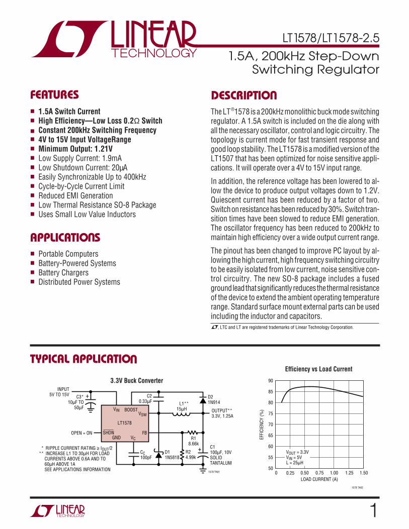
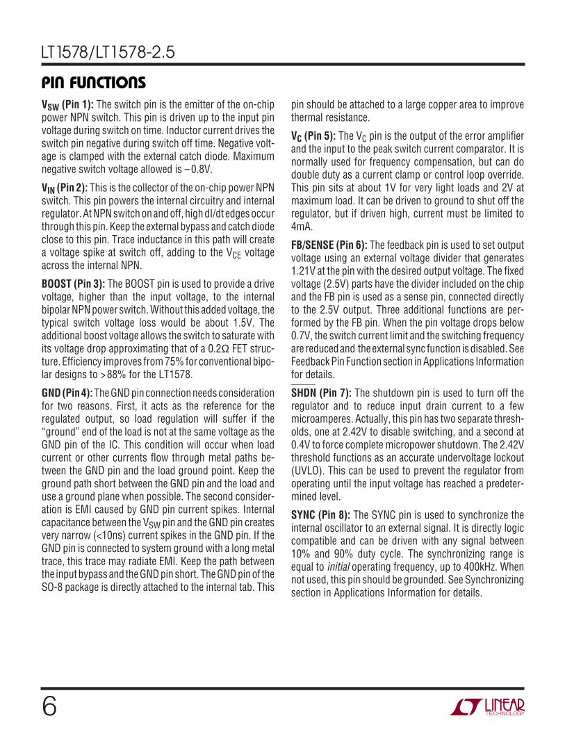
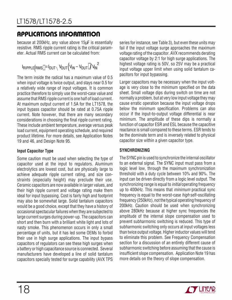
1 LT1578/LT1578-2.5 1.5A, 200kHz Step-Down Switching Regulator 3.3V Buck Converter Efficiency vs Load Current ■ 1.5A Switch Current ■ High Efficiency—Low Loss 0.2Ω Switch ■ Constant 200kHz Switching Frequency ■ 4V to 15V Input VoltageRange ■ Minimum Output: 1.21V ■ Low Supply Current: 1.9mA ■ Low Shutdown Current: 20μ A ■ Easily Synchronizable Up to 400kHz ■ Cycle-by-Cycle Current Limit ■ Reduced EMI Generation ■ Low Thermal Resistance SO-8 Package ■ Uses Small Low Value Inductors The LT ® 1578 is a 200kHz monolithic buck mode switching regulator. A 1.5A switch is included on the die along with all the necessary oscillator, control and logic circuitry. The topology is current mode for fast transient response and good loop stability. The LT1578 is a modified version of the LT1507 that has been optimized for noise sensitive appli- cations. It will operate over a 4V to 15V input range. In addition, the reference voltage has been lowered to al- low the device to produce output voltages down to 1.2V. Quiescent current has been reduced by a factor of two. Switch on resistance has been reduced by 30%. Switch tran- sition times have been slowed to reduce EMI generation. The oscillator frequency has been reduced to 200kHz to maintain high efficiency over a wide output current range. The pinout has been changed to improve PC layout by al- lowing the high current, high frequency switching circuitry to be easily isolated from low current, noise sensitive con- trol circuitry. The new SO-8 package includes a fused ground lead that significantly reduces the thermal resistance of the device to extend the ambient operating temperature range. Standard surface mount external parts can be used including the inductor and capacitors. ■ Portable Computers ■ Battery-Powered Systems ■ Battery Chargers ■ Distributed Power Systems , LTC and LT are registered trademarks of Linear Technology Corporation. LOAD CURRENT (A) 0 EFFICIENCY (%) 90 85 80 75 70 65 60 55 50 0.25 0.50 0.75 1.00 1578 TA02 1.25 1.50 V OUT = 3.3V V IN = 5V L = 25μH DESCRIPTIO U FEATURES APPLICATIO S U BOOST LT1578 V IN SHDN OUTPUT** 3.3V, 1.25A * RIPPLE CURRENT RATING ≥ I OUT /2 ** INCREASE L1 TO 30μH FOR LOAD CURRENTS ABOVE 0.6A AND TO 60μH ABOVE 1A SEE APPLICATIONS INFORMATION INPUT 5V TO 15V 1578 TA01 C2 0.33μF C C 100pF D1 1N5818 C1 100μF, 10V SOLID TANTALUM C3* 10μF TO 50μF OPEN = ON D2 1N914 L1** 15μH V SW FB GND V C + + R2 4.99k R1 8.66k TYPICAL APPLICATION U
-
Upload
nguyenmien -
Category
Documents
-
view
215 -
download
1
Transcript of FEATURES DESCRIPTIO U - Farnell element14 · · 2011-02-21Uses Small Low Value Inductors ......
1
LT1578/LT1578-2.5
1.5A, 200kHz Step-Down Switching Regulator
3.3V Buck Converter
Efficiency vs Load Current
1.5A Switch Current High Efficiency—Low Loss 0.2Ω Switch Constant 200kHz Switching Frequency 4V to 15V Input VoltageRange Minimum Output: 1.21V Low Supply Current: 1.9mA Low Shutdown Current: 20µA Easily Synchronizable Up to 400kHz Cycle-by-Cycle Current Limit Reduced EMI Generation Low Thermal Resistance SO-8 Package Uses Small Low Value Inductors
The LT®1578 is a 200kHz monolithic buck mode switchingregulator. A 1.5A switch is included on the die along withall the necessary oscillator, control and logic circuitry. Thetopology is current mode for fast transient response andgood loop stability. The LT1578 is a modified version of theLT1507 that has been optimized for noise sensitive appli-cations. It will operate over a 4V to 15V input range.
In addition, the reference voltage has been lowered to al-low the device to produce output voltages down to 1.2V.Quiescent current has been reduced by a factor of two.Switch on resistance has been reduced by 30%. Switch tran-sition times have been slowed to reduce EMI generation.The oscillator frequency has been reduced to 200kHz tomaintain high efficiency over a wide output current range.
The pinout has been changed to improve PC layout by al-lowing the high current, high frequency switching circuitryto be easily isolated from low current, noise sensitive con-trol circuitry. The new SO-8 package includes a fusedground lead that significantly reduces the thermal resistanceof the device to extend the ambient operating temperaturerange. Standard surface mount external parts can be usedincluding the inductor and capacitors.
Portable Computers Battery-Powered Systems Battery Chargers Distributed Power Systems
, LTC and LT are registered trademarks of Linear Technology Corporation.
LOAD CURRENT (A)0
EFFI
CIEN
CY (%
)
90
85
80
75
70
65
60
55
500.25 0.50 0.75 1.00
1578 TA02
1.25 1.50
VOUT = 3.3VVIN = 5VL = 25µH
DESCRIPTIO
U
FEATURES
APPLICATIO SU
BOOST
LT1578
VIN
SHDN
OUTPUT**3.3V, 1.25A
* RIPPLE CURRENT RATING ≥ IOUT/2** INCREASE L1 TO 30µH FOR LOAD
CURRENTS ABOVE 0.6A AND TO 60µH ABOVE 1A SEE APPLICATIONS INFORMATION
INPUT5V TO 15V
1578 TA01
C20.33µF
CC100pF
D11N5818
C1100µF, 10VSOLIDTANTALUM
C3*10µF TO
50µF
OPEN = ON
D21N914 L1**
15µHVSW
FBGND VC
+
+R24.99k
R18.66k
TYPICAL APPLICATION
U
2
LT1578/LT1578-2.5
PARAMETER CONDITIONS MIN TYP MAX UNITSFeedback Voltage 1.195 1.21 1.225 V
All Conditions 1.18 1.24 VSense Voltage (Fixed 2.5) 2.46 2.5 2.54 V
All Conditions 2.44 2.56 VSense Pin Resistance 5.7 9.5 13.7 kΩReference Voltage Line Regulation 4.3V ≤ VIN ≤ 15V 0.01 0.03 %/VFeedback Input Bias Current 0.5 2 µAError Amplifier Voltage Gain (Notes 2, 10) 200 400Error Amplifier Transconductance (Note 10) ∆I (VC) = ±10µA 800 1050 1300 µMho
400 1700 µMhoVC Pin to Switch Current Transconductance 1.5 A/VError Amplifier Source Current VFB = 1.1V 40 110 190 µAError Amplifier Sink Current VFB = 1.4V 50 130 200 µAVC Pin Switching Threshold Duty Cycle = 0 0.8 VVC Pin High Clamp 2.1 VSwitch Current Limit VC Open, VFB = 1.1V, DC ≤ 50% 1.5 2 3.5 ASlope Compensation (Note 8) DC = 80% 0.3 ASwitch On Resistance (Note 7) ISW = 1.5A 0.2 0.35 Ω
0.45 ΩMaximum Switch Duty Cycle VFB = 1.1V 90 94 %
86 94 %Minimum Switch Duty Cycle (Note 9) 8 %Switch Frequency VC Set to Give 50% Duty Cycle 180 200 220 kHz
160 240 kHzSwitch Frequency Line Regulation 4.3V ≤ VIN ≤ 15V 0 0.15 %/VFrequency Shifting Threshold on FB Pin ∆f = 10kHz 0.4 0.74 1.0 VMinimum Input Voltage (Note 3) 4.0 4.3 VMinimum Boost Voltage (Note 4) ISW ≤ 1.5A 2.3 3.0 V
ABSOLUTE MAXIMUM RATINGS
W WW U
PACKAGE/ORDER INFORMATION
W UU
(Note 1)
Input Voltage .......................................................... 16VBOOST Pin Above Input Voltage ............................. 10VSHDN Pin Voltage ..................................................... 7VSENSE Pin Voltage .................................................... 4VFB Pin Voltage (Adjustable Part) ............................ 3.5VFB Pin Current (Adjustable Part) ............................ 1mASYNC Pin Voltage ..................................................... 7VOperating Junction Temperature Range
LT1578C ............................................... 0°C to 125° CLT1578I ........................................... – 40°C to 125°C
Storage Temperature Range ................ – 65°C to 150°CLead Temperature (Soldering, 10 sec)................. 300°C
The denotes specifications which apply over the full operating tempera-ture range, otherwise specifications are at TJ = 25°C. VIN = 5V, VC = 1.5V, Boost = VIN + 5V, switch open, unless otherwise noted.ELECTRICAL CHARACTERISTICS
Consult factory for Military grade parts.
ORDER PARTNUMBER
LT1578CS8LT1578IS8LT1578CS8-2.5LT1578IS8-2.5
S8 PART MARKING
15781578I
1
2
3
4
8
7
6
5
TOP VIEW
S8 PACKAGE8-LEAD PLASTIC SO
VSW
VIN
BOOST
GND
SHDN
FB/SENSE
VC
SYNC
θJA = 80°C/ W WITH FUSED GROUND PINCONNECTED TO GROUND PLANE ORLARGE LANDS 157825
578I25
3
LT1578/LT1578-2.5
PARAMETER CONDITIONS MIN TYP MAX UNITSBoost Current (Note 5) ISW = 0.5A 9 18 mA
ISW = 1.5A 27 50 mAVIN Supply Current (Note 6) 1.9 2.7 mAShutdown Supply Current VSHDN = 0V, VIN ≤ 15V, VSW = 0V, VC Open 20 50 µA
75 µALockout Threshold VC Open 2.34 2.42 2.50 VShutdown Thresholds VC Open Device Shutting Down 0.13 0.37 0.60 V
Device Starting Up 0.25 0.45 0.7 VSynchronization Threshold 1.5 2.2 VSynchronizing Range 250 400 kHzSYNC Pin Input Resistance 40 kΩ
Note 1: Absolute Maximum Ratings are those values beyond which the lifeof a device may be impaired.Note 2: Gain is measured with a VC swing equal to 200mV above theswitching threshold level to 200mV below the upper clamp level.Note 3: Minimum input voltage is not measured directly, but is guaranteedby other tests. It is defined as the voltage where internal bias lines are stillregulated so that the reference voltage and oscillator frequency remainconstant. Actual minimum input voltage to maintain a regulated output willdepend on output voltage and load current. See Applications Information.Note 4: This is the minimum voltage across the boost capacitor needed toguarantee full saturation of the internal power switch.Note 5: Boost current is the current flowing into the boost pin with the pinheld 5V above input voltage. It flows only during switch on time.Note 6: Input supply current is the bias current drawn by the input pinwith switching disabled.
Note 7: Switch on resistance is calculated by dividing VIN to VSW voltageby the forced current (1.5A). See Typical Performance Characteristics forthe graph of switch voltage at other currents.Note 8: Slope compensation is the current subtracted from the switchcurrent limit at 80% duty cycle. See Maximum Output Load Current in theApplications Information section for further details.Note 9: Minimum on-time is 400ns typical. For a 200kHz operatingfrequency this means the minimum duty cycle is 8%. In frequencyfoldback mode, the effective duty cycle will be less than 8%.Note 10: Transconductance and voltage gain refer to the internal amplifierexclusive of the voltage divider. To calculate gain and transconductancereferred to the sense pin on the fixed voltage parts, divide values shown bythe ratio 2.5/1.21.
TYPICAL PERFORMANCE CHARACTERISTICS
UW
Switch Voltage Drop
JUNCTION TEMPERATURE (°C)–50
1.23
1.22
1.21
1.20
1.19100
1576 G03
–25 0 25 50 75 125
FEED
BACK
VOL
TAGE
(V)
SWITCH CURRENT (A)0
SWIT
CH V
OLTA
GE (V
)
0.5
0.4
0.3
0.2
0.1
00.25 0.50 0.75 1.00
1576 G01
1.25 1.50
125°C
–20°C
25°C
Feedback Pin VoltageSwitch Peak Current Limit
DUTY CYCLE (%)0
SWIT
CH P
EAK
CURR
ENT
(A)
2.5
2.0
1.5
1.0
0.5
080
1576 G02
20 40 60 100
TYPICAL
MINIMUM
The denotes specifications which apply over the full operating tempera-ture range, otherwise specifications are at TJ = 25°C. VIN = 5V, VC = 1.5V, Boost = VIN + 5V, switch open, unless otherwise noted.ELECTRICAL CHARACTERISTICS
4
LT1578/LT1578-2.5
TYPICAL PERFORMANCE CHARACTERISTICS
UW
JUNCTION TEMPERATURE (°C)–50
4
3
2
1
0100
1576 G04
–25 0 25 50 75 125
SHDN
PIN
CUR
RENT
(µA)
AT 2.44V STANDBY THRESHOLD(CURRENT FLOWS OUT OF PIN)
Shutdown Pin Bias Current(VSHDN = Lockout Threshold)
JUNCTION TEMPERATURE (°C)–50
180
160
140
120
100
80
60
40
20
0100
1576 G05
–25 0 25 50 75 125
SHDN
PIN
CUR
RENT
(µA)
CURRENT REQUIRED TO FORCE SHUTDOWN (FLOWS OUT OF PIN).AFTER SHUTDOWN, CURRENTDROPS TO A FEW µA
JUNCTION TEMPERATURE (°C)–50
SHUT
DOW
N PI
N VO
LTAG
E (V
)
100
1576 G06
0 50
0.8
0.7
0.6
0.5
0.4
0.3
0.2
0.1
0–25 25 75 125
START-UP
SHUTDOWN
Shutdown Supply Current
INPUT VOLTAGE (V)0
INPU
T SU
PPLY
CUR
RENT
(µA)
25
20
15
10
5
0
1576 G08
5 10 15
VSHDN = 0V
FREQUENCY (Hz)
GAIN
(µM
ho) PHASE (DEG)
2000
1500
1000
500
0
–500
200
150
100
50
0
–5010 1k 10k 1M
1576 G09
100 100k
GAIN
PHASE
ERROR AMPLIFIER EQUIVALENT CIRCUIT
ROUT570k
COUT2.4pF
VC
RLOAD = 50Ω
VFB 1 × 10⁻³)(
Error Amplifier Transconductance
JUNCTION TEMPERATURE (°C)–50
SHUT
DOW
N PI
N VO
LTAG
E (V
)
2.46
2.45
2.44
2.43
2.42
2.41
2.4025 75
1576 G07
–25 0 50 100 125
ON
STANDBY
FEEDBACK VOLTAGE (V)0
SWIT
CHIN
G FR
EQUE
NCY
(kHz
)OR
CUR
RENT
(µA)
2.0
1576 G12
0.5 1.0 1.5
250
200
150
100
50
0FEEDBACK PIN CURRENT
SWITCHING FREQUENCY
Shutdown Supply Current
JUNCTION TEMPERATURE (°C)–50
TRAN
SCON
DUCT
ANCE
(µM
ho)
100
1576 G11
0 50
1600
1400
1200
1000
800
600
400
200
0–25 25 75 125
Error Amplifier Transconductance Frequency Foldback
Shutdown Thresholds
Standby Thresholds
SHUTDOWN VOLTAGE (V)0
INPU
T SU
PPLY
CUR
RENT
(µA)
30
25
20
15
10
5
0
1576 G010
0.1 0.2 0.3 0.4
VIN = 10V
Shutdown Pin Bias Current(VSHDN = Shutdown Threshold)
5
LT1578/LT1578-2.5
TYPICAL PERFORMANCE CHARACTERISTICS
UWKool Mµ is a registered trademark of Magnetics, Inc.Metglas is a registered trademark of AlliedSignal, Inc.
JUNCTION TEMPERATURE (°C)–50
240
220
200
180
160100
1576 G13
–25 0 25 50 75 125
FREQ
UENC
Y (k
Hz)
Switching Frequency
INPUT VOLTAGE (V)6
OUTP
UT C
URRE
NT (A
)
0.6
0.8
1.0
1578 G15
0.4
0.2
09 12
1.2
L = 60µH1.4
1.6
15
L = 30µH
L = 15µH
Maximum Output Currentat VOUT = 5V
LOAD CURRENT (mA)1
INPU
T VO
LTAG
E (V
)
4.50
4.25
4.00
3.75
3.5010 100 1000
1576 G14
Minimum Input Voltage to Startwith 3.3V Output
INPUT VOLTAGE (V)4
OUTP
UT C
URRE
NT (A
)
0.6
0.8
1.0
1578 G16
0.4
0.2
06 8 10 12
1.2
1.4
1.6
14
L = 30µH
L = 15µH
L = 60µH
Maximum Output Currentat VOUT = 3.3V
INPUT VOLTAGE (V)4
OUTP
UT C
URRE
NT (A
)
0.6
0.8
1.0
1578 G17
0.4
0.2
06 8 10 12
1.2
1.4
1.6
14
L = 30µH
L = 15µH
L = 60µH
Maximum Output Currentat VOUT = 2.5V
BOOST Pin Current VC Pin Shutdown Threshold
SWITCH CURRENT (A)0
BOOS
T PI
N CU
RREN
T (m
A)
30
25
20
15
10
5
00.25 0.50 0.75 1.00
1576 G20
1.25 1.50
JUNCTION TEMPERATURE (°C)–50
1.0
0.8
0.6
0.4
0.2
0100
1576 G21
–25 0 25 50 75 125
THRE
SHOL
D VO
LTAG
E (V
)
FEEDBACK PIN VOLTAGE (V)0
0
SWIT
CH C
URRE
NT L
IMIT
(A)
0.5
1.0
1.5
2.0
3.0
0.2 0.4 0.6 0.8
1578 G19
1.0 1.2
2.5
Switch Current Limit Foldback
6
LT1578/LT1578-2.5
PIN FUNCTIONS
UUU
VSW (Pin 1): The switch pin is the emitter of the on-chippower NPN switch. This pin is driven up to the input pinvoltage during switch on time. Inductor current drives theswitch pin negative during switch off time. Negative volt-age is clamped with the external catch diode. Maximumnegative switch voltage allowed is –0.8V.
VIN (Pin 2): This is the collector of the on-chip power NPNswitch. This pin powers the internal circuitry and internalregulator. At NPN switch on and off, high dI/dt edges occurthrough this pin. Keep the external bypass and catch diodeclose to this pin. Trace inductance in this path will createa voltage spike at switch off, adding to the VCE voltageacross the internal NPN.
BOOST (Pin 3): The BOOST pin is used to provide a drivevoltage, higher than the input voltage, to the internalbipolar NPN power switch. Without this added voltage, thetypical switch voltage loss would be about 1.5V. Theadditional boost voltage allows the switch to saturate withits voltage drop approximating that of a 0.2Ω FET struc-ture. Efficiency improves from 75% for conventional bipo-lar designs to >88% for the LT1578.
GND (Pin 4): The GND pin connection needs considerationfor two reasons. First, it acts as the reference for theregulated output, so load regulation will suffer if the“ground” end of the load is not at the same voltage as theGND pin of the IC. This condition will occur when loadcurrent or other currents flow through metal paths be-tween the GND pin and the load ground point. Keep theground path short between the GND pin and the load anduse a ground plane when possible. The second consider-ation is EMI caused by GND pin current spikes. Internalcapacitance between the VSW pin and the GND pin createsvery narrow (<10ns) current spikes in the GND pin. If theGND pin is connected to system ground with a long metaltrace, this trace may radiate EMI. Keep the path betweenthe input bypass and the GND pin short. The GND pin of theSO-8 package is directly attached to the internal tab. This
pin should be attached to a large copper area to improvethermal resistance.
VC (Pin 5): The VC pin is the output of the error amplifierand the input to the peak switch current comparator. It isnormally used for frequency compensation, but can dodouble duty as a current clamp or control loop override.This pin sits at about 1V for very light loads and 2V atmaximum load. It can be driven to ground to shut off theregulator, but if driven high, current must be limited to4mA.
FB/SENSE (Pin 6): The feedback pin is used to set outputvoltage using an external voltage divider that generates1.21V at the pin with the desired output voltage. The fixedvoltage (2.5V) parts have the divider included on the chipand the FB pin is used as a sense pin, connected directlyto the 2.5V output. Three additional functions are per-formed by the FB pin. When the pin voltage drops below0.7V, the switch current limit and the switching frequencyare reduced and the external sync function is disabled. SeeFeedback Pin Function section in Applications Informationfor details.
SHDN (Pin 7): The shutdown pin is used to turn off theregulator and to reduce input drain current to a fewmicroamperes. Actually, this pin has two separate thresh-olds, one at 2.42V to disable switching, and a second at0.4V to force complete micropower shutdown. The 2.42Vthreshold functions as an accurate undervoltage lockout(UVLO). This can be used to prevent the regulator fromoperating until the input voltage has reached a predeter-mined level.
SYNC (Pin 8): The SYNC pin is used to synchronize theinternal oscillator to an external signal. It is directly logiccompatible and can be driven with any signal between10% and 90% duty cycle. The synchronizing range isequal to initial operating frequency, up to 400kHz. Whennot used, this pin should be grounded. See Synchronizingsection in Applications Information for details.
7
LT1578/LT1578-2.5
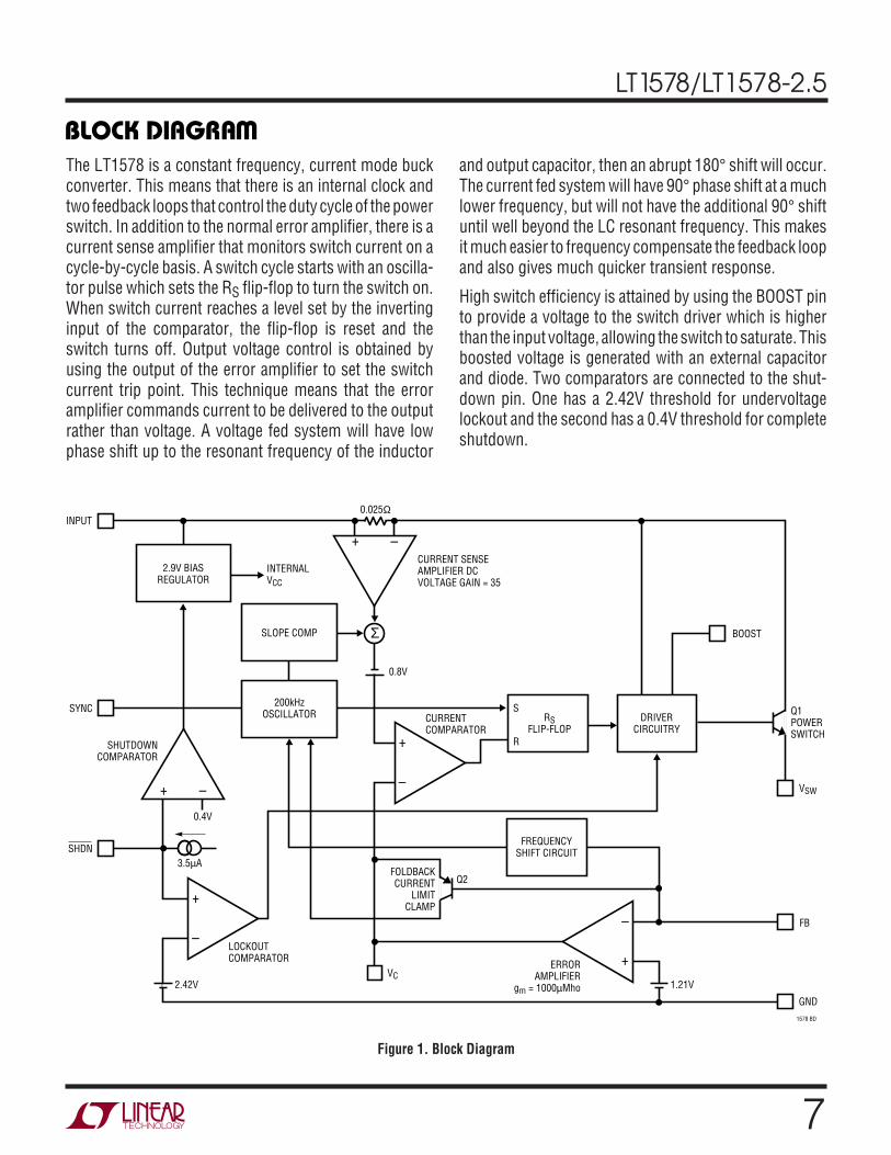
BLOCK DIAGRAM
W
and output capacitor, then an abrupt 180° shift will occur.The current fed system will have 90° phase shift at a muchlower frequency, but will not have the additional 90° shiftuntil well beyond the LC resonant frequency. This makesit much easier to frequency compensate the feedback loopand also gives much quicker transient response.
High switch efficiency is attained by using the BOOST pinto provide a voltage to the switch driver which is higherthan the input voltage, allowing the switch to saturate. Thisboosted voltage is generated with an external capacitorand diode. Two comparators are connected to the shut-down pin. One has a 2.42V threshold for undervoltagelockout and the second has a 0.4V threshold for completeshutdown.
The LT1578 is a constant frequency, current mode buckconverter. This means that there is an internal clock andtwo feedback loops that control the duty cycle of the powerswitch. In addition to the normal error amplifier, there is acurrent sense amplifier that monitors switch current on acycle-by-cycle basis. A switch cycle starts with an oscilla-tor pulse which sets the RS flip-flop to turn the switch on.When switch current reaches a level set by the invertinginput of the comparator, the flip-flop is reset and theswitch turns off. Output voltage control is obtained byusing the output of the error amplifier to set the switchcurrent trip point. This technique means that the erroramplifier commands current to be delivered to the outputrather than voltage. A voltage fed system will have lowphase shift up to the resonant frequency of the inductor
–
+
–
+
–
+
–+
Σ
INPUT
2.9V BIASREGULATOR
200kHzOSCILLATOR
FREQUENCYSHIFT CIRCUIT
VSW
FB
VC
LOCKOUTCOMPARATOR
GND1578 BD
SLOPE COMP
0.025Ω
INTERNALVCC
CURRENT SENSEAMPLIFIER DC VOLTAGE GAIN = 35
SYNC
SHDN
SHUTDOWNCOMPARATOR
CURRENTCOMPARATOR
ERRORAMPLIFIER
gm = 1000µMho
FOLDBACKCURRENT
LIMITCLAMP
BOOST
RSFLIP-FLOP
DRIVERCIRCUITRY
S
R
0.8V
Q2
Q1POWERSWITCH
1.21V2.42V
–+
0.4V
3.5µA
Figure 1. Block Diagram
8
LT1578/LT1578-2.5
APPLICATIONS INFORMATION
WU UU
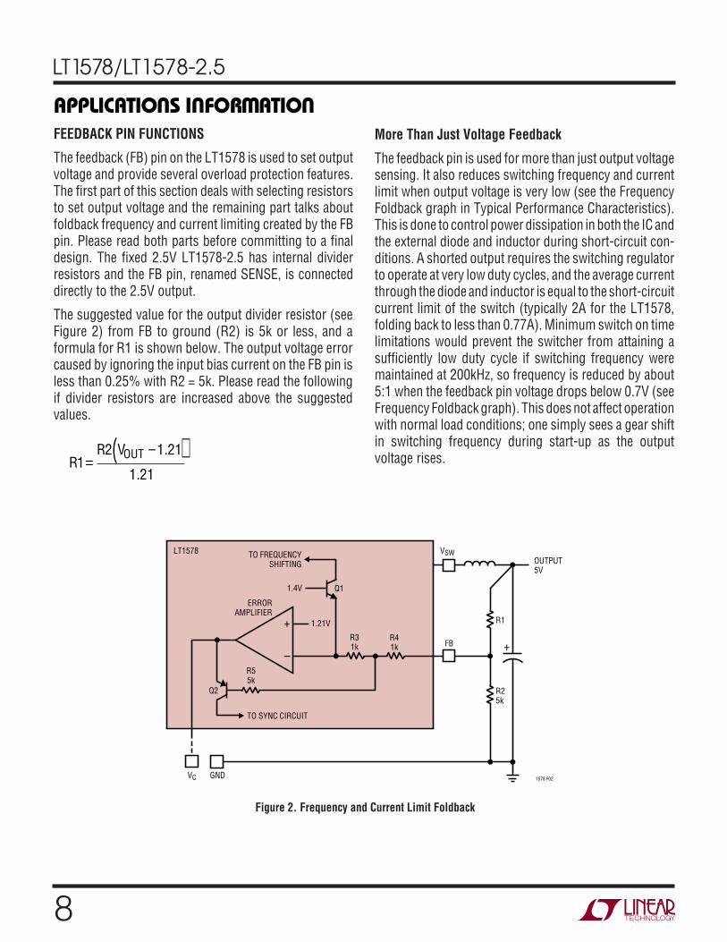
Figure 2. Frequency and Current Limit Foldback
–
+ 1.21V
VSW
VC GND
TO SYNC CIRCUIT
1578 F02
TO FREQUENCYSHIFTING
R31k
R41k
R1
R25k
OUTPUT5V
R55k
ERRORAMPLIFIER
FB
1.4V Q1
LT1578
Q2
+
FEEDBACK PIN FUNCTIONS
The feedback (FB) pin on the LT1578 is used to set outputvoltage and provide several overload protection features.The first part of this section deals with selecting resistorsto set output voltage and the remaining part talks aboutfoldback frequency and current limiting created by the FBpin. Please read both parts before committing to a finaldesign. The fixed 2.5V LT1578-2.5 has internal dividerresistors and the FB pin, renamed SENSE, is connecteddirectly to the 2.5V output.
The suggested value for the output divider resistor (seeFigure 2) from FB to ground (R2) is 5k or less, and aformula for R1 is shown below. The output voltage errorcaused by ignoring the input bias current on the FB pin isless than 0.25% with R2 = 5k. Please read the followingif divider resistors are increased above the suggestedvalues.
RR VOUT
12 1 21
1 21=
−( ).
.
More Than Just Voltage Feedback
The feedback pin is used for more than just output voltagesensing. It also reduces switching frequency and currentlimit when output voltage is very low (see the FrequencyFoldback graph in Typical Performance Characteristics).This is done to control power dissipation in both the IC andthe external diode and inductor during short-circuit con-ditions. A shorted output requires the switching regulatorto operate at very low duty cycles, and the average currentthrough the diode and inductor is equal to the short-circuitcurrent limit of the switch (typically 2A for the LT1578,folding back to less than 0.77A). Minimum switch on timelimitations would prevent the switcher from attaining asufficiently low duty cycle if switching frequency weremaintained at 200kHz, so frequency is reduced by about5:1 when the feedback pin voltage drops below 0.7V (seeFrequency Foldback graph). This does not affect operationwith normal load conditions; one simply sees a gear shiftin switching frequency during start-up as the outputvoltage rises.
9
LT1578/LT1578-2.5
APPLICATIONS INFORMATION
WU UU
In addition to lower switching frequency, the LT1578 alsooperates at lower switch current limit when the feedbackpin voltage drops below 0.7V. Q2 in Figure 2 performs thisfunction by clamping the VC pin to a voltage less than itsnormal 2.1V upper clamp level. This foldback current limitgreatly reduces power dissipation in the IC, diode andinductor during short-circuit conditions. External synchro-nization is also disabled to prevent interference withfoldback operation. Again, it is nearly transparent to theuser under normal load conditions. The only loads that maybe affected are current sources, such as lamps and mo-tors, that maintain high load current with output voltageless than 50% of final value. In these rare situations thefeedback pin can be clamped above 0.7V to defeat foldbackcurrent limit. Caution: clamping the feedback pin meansthat frequency shifting will also be defeated, so a combina-tion of high input voltage and dead shorted output maycause the LT1578 to lose control of current limit.
The internal circuitry which forces reduced switchingfrequency also causes current to flow out of the feedbackpin when output voltage is low. The equivalent circuitry isshown in Figure 2. Q1 is completely off during normaloperation. If the FB pin falls below 0.7V, Q1 begins toconduct current and reduces frequency at the rate ofapproximately 1kHz/µA. To ensure adequate frequencyfoldback (under worst-case short-circuit conditions), theexternal divider Thevinin resistance must be low enoughto pull 35µA out of the FB pin with 0.5V on the pin (RDIV ≤14.3k). The net result is that reductions in frequency andcurrent limit are affected by output voltage divider imped-ance. Although divider impedance is not critical, cautionshould be used if resistors are increased beyond thesuggested values and short-circuit conditions will occurwith high input voltage. High frequency pickup willincrease and the protection accorded by frequency andcurrent foldback will decrease.
MAXIMUM OUTPUT LOAD CURRENT
Maximum load current for a buck converter is limited bythe maximum switch current rating (IP) of the LT1578.This current rating is 1.5A up to 50% duty cycle (DC),decreasing to 1.3A at 80% duty cycle. This is shown
graphically in Typical Performance Characteristics and asshown in the formula below:
IP = 1.5A for DC ≤ 50%IP = 1.67 – 0.18 (DC) – 0.32(DC)2 for 50% < DC < 90%
DC = Duty cycle = VOUT/VIN
Example: with VOUT = 5V, VIN = 8V; DC = 5/8 = 0.625, and;
ISW(MAX) = 1.67 – 0.18 (0.625) – 0.32(0.625)2 = 1.43A
Current rating decreases with duty cycle because theLT1578 has internal slope compensation to prevent cur-rent mode subharmonic switching. For more details, readApplication Note 19. The LT1578 is a little unusual in thisregard because it has nonlinear slope compensation whichgives better compensation with less reduction in currentlimit.
Maximum load current would be equal to maximumswitch current for an infinitely large inductor, but withfinite inductor size, maximum load current is reduced byone-half peak-to-peak inductor current. The followingformula assumes continuous mode operation, implyingthat the term on the right is less than one-half of IP.
IOUT(MAX) =Continuous Mode
For the conditions above and L = 15µH,
I
A
OUT MAX( ) −= −
( ) −( )
( )
= − =
1 435 8 5
2 15 10 200 10 8
1 43 0 31 1 12
6 3.
• •
. . .
At VIN = 15V, duty cycle is 33%, so IP is just equal to a fixed1.5A, and IOUT(MAX) is equal to:
1 55 15 5
2 15 10 200 10 15
1 5 0 56 0 94
6 3.
• •
. . .
−( ) −( )
( )
= − =
−
A
I P −( ) −( )
( )( )( )V V V
L f V
OUT IN OUT
IN2
10
LT1578/LT1578-2.5
Note that there is less load current available at the higherinput voltage because inductor ripple current increases.This is not always the case. Certain combinations ofinductor value and input voltage range may yield loweravailable load current at the lowest input voltage due toreduced peak switch current at high duty cycles. If loadcurrent is close to the maximum available, please checkmaximum available current at both input voltageextremes. To calculate actual peak switch current with agiven set of conditions, use:
I IV V V
L f VSW PEAK OUT
OUT IN OUT
IN( ) = +
−( )( )( )( )2
For lighter loads where discontinuous operation can beused, maximum load current is equal to:
IOUT(MAX) =Discontinuous mode
Example: with L = 5µH, VOUT = 5V, and VIN(MAX) = 15V,
I AOUT MAX( )−
=( )
( )
( ) −( ) =1 5 200 10 5 10 15
2 5 15 50 34
2 3 6. • •.
The main reason for using such a tiny inductor is that it isphysically very small, but keep in mind that peak-to-peakinductor current will be very high. This will increase outputripple voltage. If the output capacitor has to be made largerto reduce ripple voltage, the overall circuit could actuallywind up larger.
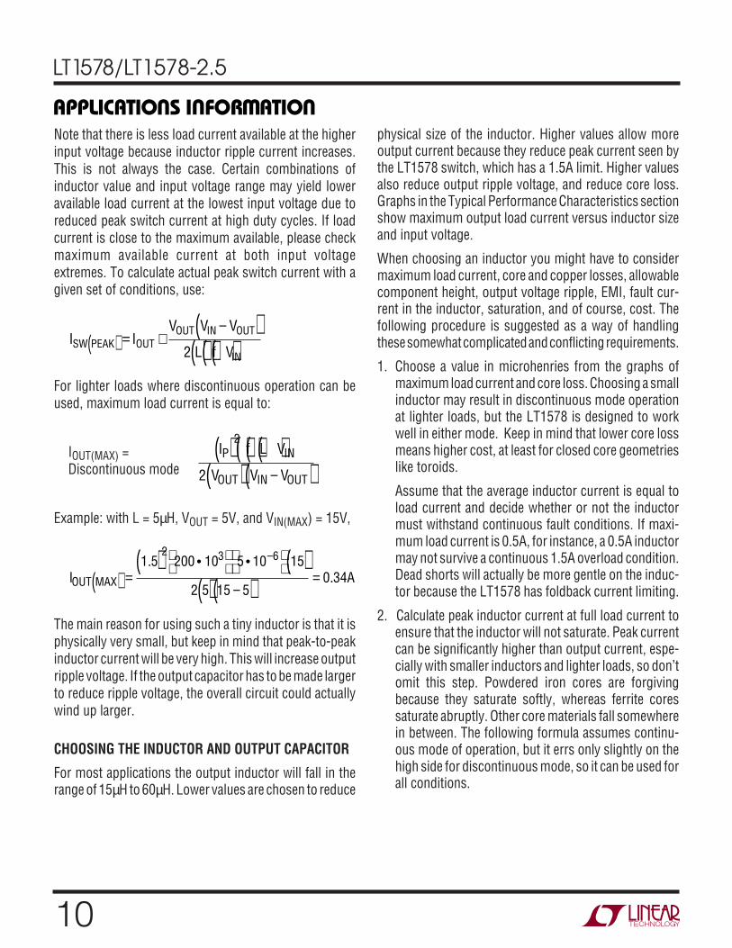
CHOOSING THE INDUCTOR AND OUTPUT CAPACITOR
For most applications the output inductor will fall in therange of 15µH to 60µH. Lower values are chosen to reduce
APPLICATIONS INFORMATION
WU UU
physical size of the inductor. Higher values allow moreoutput current because they reduce peak current seen bythe LT1578 switch, which has a 1.5A limit. Higher valuesalso reduce output ripple voltage, and reduce core loss.Graphs in the Typical Performance Characteristics sectionshow maximum output load current versus inductor sizeand input voltage.
When choosing an inductor you might have to considermaximum load current, core and copper losses, allowablecomponent height, output voltage ripple, EMI, fault cur-rent in the inductor, saturation, and of course, cost. Thefollowing procedure is suggested as a way of handlingthese somewhat complicated and conflicting requirements.
1. Choose a value in microhenries from the graphs ofmaximum load current and core loss. Choosing a smallinductor may result in discontinuous mode operationat lighter loads, but the LT1578 is designed to workwell in either mode. Keep in mind that lower core lossmeans higher cost, at least for closed core geometrieslike toroids.
Assume that the average inductor current is equal toload current and decide whether or not the inductormust withstand continuous fault conditions. If maxi-mum load current is 0.5A, for instance, a 0.5A inductormay not survive a continuous 1.5A overload condition.Dead shorts will actually be more gentle on the induc-tor because the LT1578 has foldback current limiting.
2. Calculate peak inductor current at full load current toensure that the inductor will not saturate. Peak currentcan be significantly higher than output current, espe-cially with smaller inductors and lighter loads, so don’tomit this step. Powdered iron cores are forgivingbecause they saturate softly, whereas ferrite coressaturate abruptly. Other core materials fall somewherein between. The following formula assumes continu-ous mode of operation, but it errs only slightly on thehigh side for discontinuous mode, so it can be used forall conditions.
I f L V
V V V
P IN
OUT IN OUT
( ) ( )( )( )( ) −( )
2
2
11
LT1578/LT1578-2.5
APPLICATIONS INFORMATION
WU UU
I IV V V
f L VPEAK OUT
OUT IN OUT
IN
= +−( )
( )( )( )2
VIN = Maximum input voltagef = Switching frequency, 200kHz
3. Decide if the design can tolerate an “open” core geom-etry like a rod or barrel, with high magnetic fieldradiation, or whether it needs a closed core like a toroidto prevent EMI problems. One would not want an opencore next to a magnetic storage media, for instance!This is a tough decision because the rods or barrels aretemptingly cheap and small and there are no helpfulguidelines to calculate when the magnetic field radia-tion will be a problem.
4. Start shopping for an inductor (see representativesurface mount units in Table 1) which meets therequirements of core shape, peak current (to avoidsaturation), average current (to limit heating), and faultcurrent (if the inductor gets too hot, wire insulation willmelt and cause turn-to-turn shorts). Keep in mind thatall good things like high efficiency, low profile, and hightemperature operation will increase cost, sometimesdramatically. Get a quote on the cheapest unit first tocalibrate yourself on price, then ask for what you reallywant.
5. After making an initial choice, consider the secondarythings like output voltage ripple, second sourcing, etc.Use the experts in the Linear Technology’s applica-tions department if you feel uncertain about the finalchoice. They have experience with a wide range ofinductor types and can tell you about the latest devel-opments in low profile, surface mounting, etc.
Table 1SERIES CORE
VENDOR/ VALUE DC CORE RESIS- MATER- HEIGHTPART NO. (µH) (Amps) TYPE TANCE(Ω) IAL (mm)
Coiltronics
CTX15-2 15 1.7 Tor 0.059 KMµ 6.0
CTX33-2 33 1.4 Tor 0.106 KMµ 6.0
CTX68-4 68 1.2 Tor 0.158 KMµ 6.4
CTX15-1P 15 1.4 Tor 0.087 52 4.2
CTX33-2P 33 1.3 Tor 0.126 52 6.0
CTX68-4P 68 1.1 Tor 0.238 52 6.4
Sumida
CDRH74-150 15 1.47 SC 0.081 Fer 4.5
CDH115-330 33 1.68 SC 0.082 Fer 5.2
CDRH125-680 68 1.5 SC 0.12 Fer 6
CDH74-330 33 1.45 SC 0.17 Fer 5.2
Coilcraft
DO3308P-153 15 2 SC 0.12 Fer 3
DO3316P-333 33 2 SC 0.1 Fer 5.21
DO3316P-683 68 1.4 SC 0.18 Fer 5.21
Pulse
PE-53602 35 1.4 Tor 0.166 Fer 9.1
PE-53604 73 1.3 Tor 0.290 Fer 9.1
PE-53632 22 2.7 Tor 0.063 Fer 9.1
PE-53633 40 2.7 Tor 0.085 Fer 10
Gowanda
SMP3316-152K 15 3.5 SC 0.041 Fer 6
SMP3316-332K 33 2.3 SC 0.092 Fer 6
SMP3316-682K 68 1.7 SC 0.178 Fer 6
Tor = ToroidSC = Semi-closed geometryFer = Ferrite core material52 = Type 52 powdered iron core materialKMµ = Kool Mµ
12
LT1578/LT1578-2.5
APPLICATIONS INFORMATION
WU UU
Output Capacitor Ripple Current (RMS):
IV V V
L f VRIPPLE RMS
OUT IN OUT
IN( ) =
( ) −( )( )( )( )
0 29.
Ceramic Capacitors
Higher value, lower cost ceramic capacitors are nowbecoming available in smaller case sizes. These are tempt-ing for switching regulator use because of their very lowESR. Unfortunately, the ESR is so low that it can causeloop stability problems. Solid tantalum capacitor’s ESRgenerates a loop “zero” at 5kHz to 50kHz that is instrumen-tal in giving acceptable loop phase margin. Ceramiccapacitors remain capacitive to beyond 300kHz and usu-ally resonate with their ESL before their ESR provides anydamping. They are appropriate for input bypassing be-cause of their high ripple current ratings and tolerance ofturn-on surges.
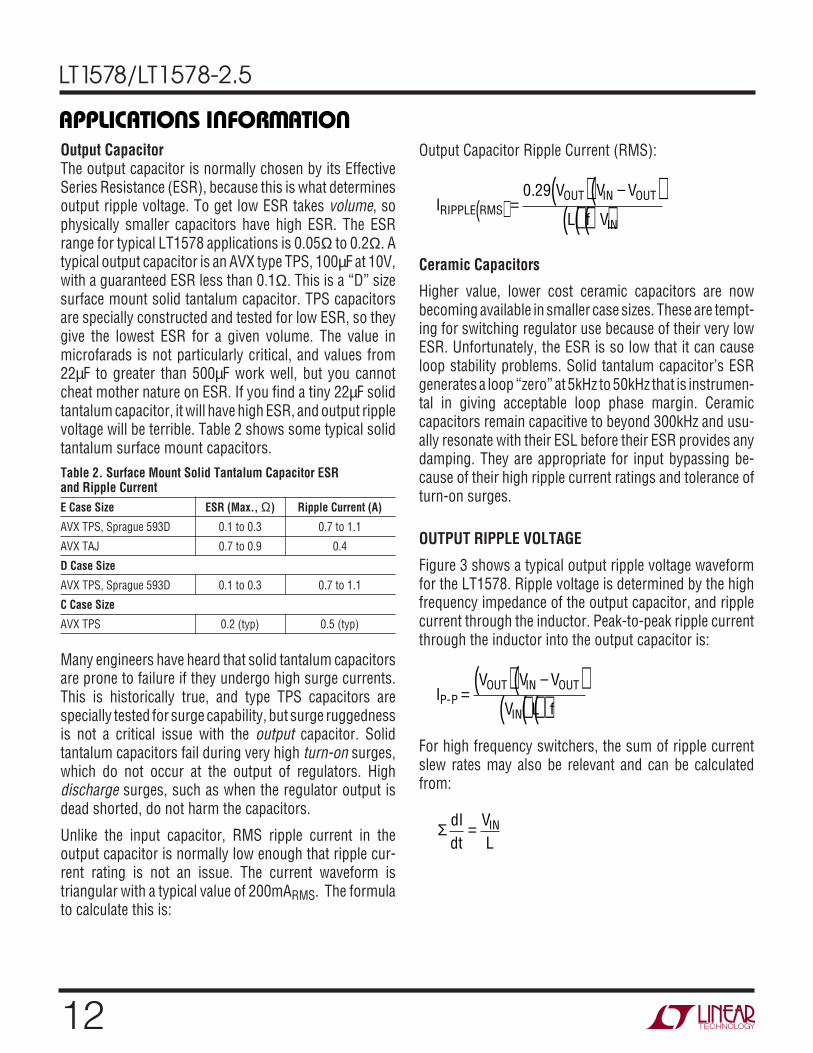
OUTPUT RIPPLE VOLTAGE
Figure 3 shows a typical output ripple voltage waveformfor the LT1578. Ripple voltage is determined by the highfrequency impedance of the output capacitor, and ripplecurrent through the inductor. Peak-to-peak ripple currentthrough the inductor into the output capacitor is:
IV V V
V L fP
OUT IN OUT
IN-P =
( ) −( )( )( )( )
For high frequency switchers, the sum of ripple currentslew rates may also be relevant and can be calculatedfrom:
Σ dIdt
VLIN=
Output CapacitorThe output capacitor is normally chosen by its EffectiveSeries Resistance (ESR), because this is what determinesoutput ripple voltage. To get low ESR takes volume, sophysically smaller capacitors have high ESR. The ESRrange for typical LT1578 applications is 0.05Ω to 0.2Ω. Atypical output capacitor is an AVX type TPS, 100µF at 10V,with a guaranteed ESR less than 0.1Ω. This is a “D” sizesurface mount solid tantalum capacitor. TPS capacitorsare specially constructed and tested for low ESR, so theygive the lowest ESR for a given volume. The value inmicrofarads is not particularly critical, and values from22µF to greater than 500µF work well, but you cannotcheat mother nature on ESR. If you find a tiny 22µF solidtantalum capacitor, it will have high ESR, and output ripplevoltage will be terrible. Table 2 shows some typical solidtantalum surface mount capacitors.Table 2. Surface Mount Solid Tantalum Capacitor ESRand Ripple CurrentE Case Size ESR (Max., Ω) Ripple Current (A)
AVX TPS, Sprague 593D 0.1 to 0.3 0.7 to 1.1
AVX TAJ 0.7 to 0.9 0.4
D Case Size
AVX TPS, Sprague 593D 0.1 to 0.3 0.7 to 1.1
C Case Size
AVX TPS 0.2 (typ) 0.5 (typ)
Many engineers have heard that solid tantalum capacitorsare prone to failure if they undergo high surge currents.This is historically true, and type TPS capacitors arespecially tested for surge capability, but surge ruggednessis not a critical issue with the output capacitor. Solidtantalum capacitors fail during very high turn-on surges,which do not occur at the output of regulators. Highdischarge surges, such as when the regulator output isdead shorted, do not harm the capacitors.
Unlike the input capacitor, RMS ripple current in theoutput capacitor is normally low enough that ripple cur-rent rating is not an issue. The current waveform istriangular with a typical value of 200mARMS. The formulato calculate this is:
13
LT1578/LT1578-2.5
APPLICATIONS INFORMATION
WU UU
CATCH DIODE
The suggested catch diode (D1) is a 1N5818 Schottky, orits Motorola equivalent, MBR130. It is rated at 1A averageforward current and 30V reverse voltage. Typical forwardvoltage is 0.42V at 1A. The diode conducts current onlyduring switch off time. Peak reverse voltage is equal toregulator input voltage. Average forward current in normaloperation can be calculated from:
2µs/DIV 1578 F03
Peak-to-peak output ripple voltage is the sum of a triwavecreated by peak-to-peak ripple current times ESR, and asquare wave created by parasitic inductance (ESL) andripple current slew rate. Capacitive reactance is assumedto be small compared to ESR or ESL.
V I ESR ESLdIdtRIPPLE = ( )( ) + ( )P-P Σ
Example: with VIN =10V, VOUT = 5V, L = 30µH, ESR = 0.1Ω,ESL = 10nH:
I A
dIdt
V A
mV
RIPPLE
P-P
P-P
=( ) −( )
( )
=
= =
= ( )( ) +
= + =
−
−
−
5 10 5
10 30 10 200 100 42
10
30 100 33 10
0 42 0 1 10 10 0 33 10
0 042 0 003 45
6 3
66
9 6
• •.
•. •
. . • . •
. .
Σ
II V V
VD AVGOUT IN OUT
IN( ) =
−( )
This formula will not yield values higher than 1A withmaximum load current of 1.25A unless the ratio of input tooutput voltage exceeds 5:1. The only reason to consider alarger diode is the worst-case condition of a high inputvoltage and overloaded (not shorted) output. Under short-circuit conditions, foldback current limit will reduce diodecurrent to less than 1A, but if the output is overloaded anddoes not fall to less than 1/3 of nominal output voltage,foldback will not take effect. With the overloaded condi-tion, output current will increase to a typical value of 1.8A,determined by peak switch current limit of 2A. WithVIN = 15V, VOUT = 4V (5V overloaded) and IOUT = 1.8A:
I AD AVG( ) =−( )
=1 8 15 4
151 32
..
This is safe for short periods of time, but it would beprudent to check with the diode manufacturer if continu-ous operation under these conditions must be tolerated.
BOOST PIN CONSIDERATIONS
For most applications, the boost components are a 0.33µFcapacitor and a 1N914 or 1N4148 diode. The anode isconnected to the regulated output voltage and this gener-ates a voltage across the boost capacitor nearly identicalto the regulated output. In certain applications, the anodemay instead be connected to the unregulated input volt-age. This could be necessary if the regulated outputvoltage is very low (< 3V) or if the input voltage is less than6V. Efficiency is not affected by the capacitor value, but thecapacitor should have an ESR of less than 1Ω to ensurethat it can be recharged fully under the worst-case condi-tion of minimum input voltage. Almost any type of film orceramic capacitor will work fine.
WARNING! Peak voltage on the BOOST pin is the sum ofunregulated input voltage plus the voltage across the
VOUT ATIOUT = 1A
INDUCTORCURRENTAT IOUT = 1A
VOUT ATIOUT = 50mA
INDUCTORCURRENTAT IOUT = 50mA
20mV/DIV
200mA/DIV
20mV/DIV
200mA/DIV
Figure 3. LT1578 Ripple Voltage Waveform
14
LT1578/LT1578-2.5
APPLICATIONS INFORMATION
WU UU
boost capacitor. This normally means that peak BOOSTpin voltage is equal to input voltage plus output voltage,but when the boost diode is connected to the regulatorinput, peak BOOST pin voltage is equal to twice the inputvoltage. Be sure that BOOST pin voltage does not exceedits maximum rating.
For nearly all applications, a 0.33µF boost capacitor worksjust fine, but for the curious, more details are providedhere. The size of the boost capacitor is determined byswitch drive current requirements. During switch on time,drain current on the capacitor is approximately IOUT/50. Atpeak load current of 1.25A, this gives a total drain of 25mA.Capacitor ripple voltage is equal to the product of on timeand drain current divided by capacitor value;∆V = (tON)(25mA/C). To keep capacitor ripple voltage toless than 0.5V (a slightly arbitrary number) at the worst-case condition of tON = 4.7µs, the capacitor needs to be0.24µF. Boost capacitor ripple voltage is not a criticalparameter, but if the minimum voltage across the capaci-tor drops to less than 3V, the power switch may notsaturate fully and efficiency will drop. An approximateformula for absolute minimum capacitor value is:
–
+
–
+
2.42V
0.4V
GND
VSW
LT1578
INPUT
RFB
RHI
1578 F04
OUTPUT
SHDN
STANDBY
IN
TOTALSHUTDOWN
3.5µA
RLOC1
+
Figure 4. Undervoltage Lockout
CI V V
f V VMIN
OUT OUT IN
OUT
=( )( )
( ) −( )/ /50
3
f = Switching frequencyVOUT = Regulated output voltageVIN = Minimum input voltage
This formula can yield capacitor values substantially lessthan 0.24µF, but it should be used with caution since itdoes not take into account secondary factors such ascapacitor series resistance, capacitance shift with tem-perature and output overload.
SHUTDOWN FUNCTION ANDUNDERVOLTAGE LOCKOUT
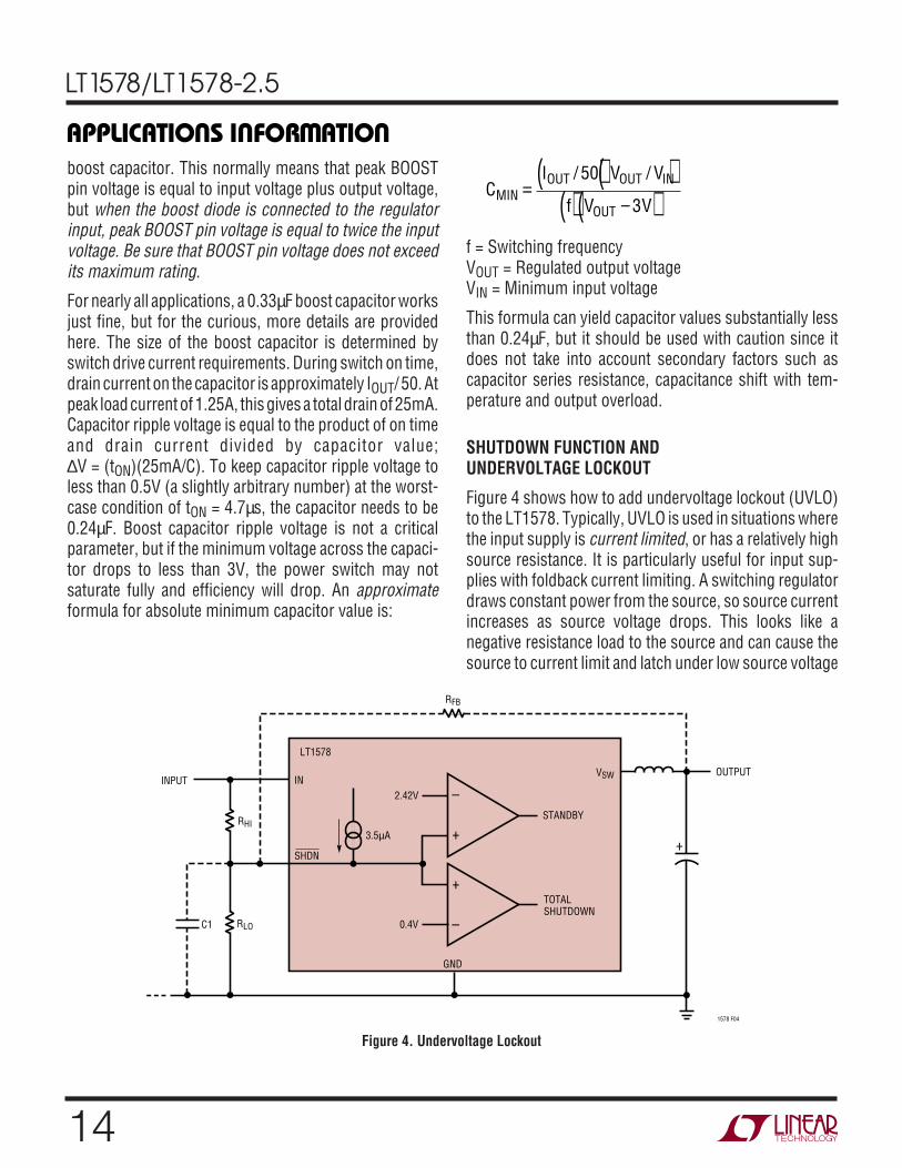
Figure 4 shows how to add undervoltage lockout (UVLO)to the LT1578. Typically, UVLO is used in situations wherethe input supply is current limited, or has a relatively highsource resistance. It is particularly useful for input sup-plies with foldback current limiting. A switching regulatordraws constant power from the source, so source currentincreases as source voltage drops. This looks like anegative resistance load to the source and can cause thesource to current limit and latch under low source voltage
15
LT1578/LT1578-2.5
conditions. UVLO helps prevent the regulator from oper-ating at source voltages where these problems mightoccur.
Threshold voltage for lockout is about 2.42V. A 3.5µA biascurrent flows out of the pin at threshold. This internallygenerated current is used to force a default high state onthe shutdown pin if the pin is left open. When low shut-down current is not an issue, the error due to this currentcan be minimized by making RLO 10k or less. If shutdowncurrent is an issue, RLO can be raised to 100k, but the errordue to initial bias current and changes with temperatureshould be considered.
R k
RR V V
V R A
LO
HILO IN
LO
= ( )=
−( )− ( )
10
2 42
2 42 3 5
to 100k 25k suggested
.
. . µ
VIN = Minimum input voltage
Keep the connections from the resistors to the shutdownpin short and make sure that interplane or surface capaci-tance to the switching nodes are minimized. If high resis-tor values are used, the shutdown pin should be bypassedwith a 1000pF capacitor to prevent coupling problemsfrom the switch node. If hysteresis is desired in theundervoltage lockout point, a resistor RFB can be added tothe output node. Resistor values can be calculated from:
RR V V V V
R A
R R V V
HILO IN OUT
LO
FB HI OUT
=− +( )+[ ]
− ( )= ( )( )
2 42 1
2 42 3 5
. /
. .
/
∆ ∆
∆
µ
25k suggested for RLOVIN = Input voltage at which switching stops as input
voltage descends to trip level∆V = Hysteresis in input voltage level
Example: output voltage is 5V, switching is to stop if inputvoltage drops below 12V and should not restart unless
APPLICATIONS INFORMATION
WU UU
input rises back to 13.5V. ∆V is therefore 1.5V andVIN = 12V. Let RLO = 25k.
Rk
k A
kk
R k k
HI
FB
=− +( ) +[ ]
− ( )=
( )=
= ( ) =
25 12 2 42 1 5 5 1 1 5
2 42 25 3 5
25 10 35
2 33111
111 5 1 5 370
. . / .
. .
.
./ .
µ
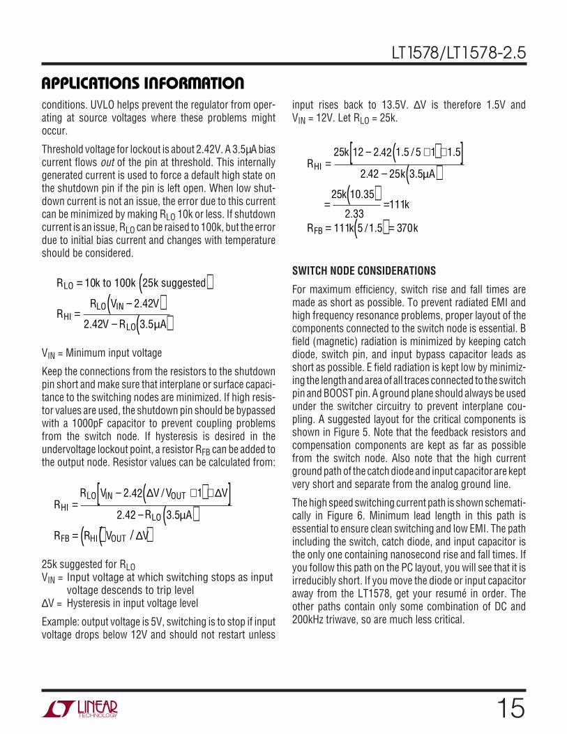
SWITCH NODE CONSIDERATIONS
For maximum efficiency, switch rise and fall times aremade as short as possible. To prevent radiated EMI andhigh frequency resonance problems, proper layout of thecomponents connected to the switch node is essential. Bfield (magnetic) radiation is minimized by keeping catchdiode, switch pin, and input bypass capacitor leads asshort as possible. E field radiation is kept low by minimiz-ing the length and area of all traces connected to the switchpin and BOOST pin. A ground plane should always be usedunder the switcher circuitry to prevent interplane cou-pling. A suggested layout for the critical components isshown in Figure 5. Note that the feedback resistors andcompensation components are kept as far as possiblefrom the switch node. Also note that the high currentground path of the catch diode and input capacitor are keptvery short and separate from the analog ground line.
The high speed switching current path is shown schemati-cally in Figure 6. Minimum lead length in this path isessential to ensure clean switching and low EMI. The pathincluding the switch, catch diode, and input capacitor isthe only one containing nanosecond rise and fall times. Ifyou follow this path on the PC layout, you will see that it isirreducibly short. If you move the diode or input capacitoraway from the LT1578, get your resumé in order. Theother paths contain only some combination of DC and200kHz triwave, so are much less critical.
16
LT1578/LT1578-2.5
APPLICATIONS INFORMATION
WU UU
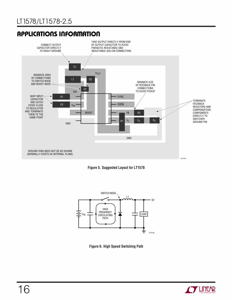
Figure 6. High Speed Switching Path
Figure 5. Suggested Layout for LT1578
VOUT
VIN
SW
BOOST FB
SYNC
SHDN
VC
GND
1578 F05
GND
KEEP INPUTCAPACITORAND CATCH
DIODE CLOSETO REGULATOR
AND TERMINATETHEM TO THESAME POINT
CONNECT OUTPUTCAPACITOR DIRECTLY
TO HEAVY GROUND
TAKE OUTPUT DIRECTLY FROM ENDOF OUTPUT CAPACITOR TO AVOIDPARASITIC RESISTANCE ANDINDUCTANCE (KELVIN CONNECTION)
MINIMIZE AREAOF CONNECTIONSTO SWITCH NODEAND BOOST NODE
GROUND RING NEED NOT BE AS SHOWN(NORMALLY EXISTS AS INTERNAL PLANE)
MINIMIZE SIZEOF FEEDBACK PIN
CONNECTIONSTO AVOID PICKUP
TERMINATE FEEDBACKRESISTORS ANDCOMPENSATIONCOMPONENTSDIRECTLY TOSWITCHERGROUND PINCC RCR1
D1
C3
D2L1
C1
C2
R2
1578 F06
5VL1
VIN
HIGHFREQUENCY
CIRCULATINGPATH
LOAD
SWITCH NODE
17
LT1578/LT1578-2.5
APPLICATIONS INFORMATION
WU UU
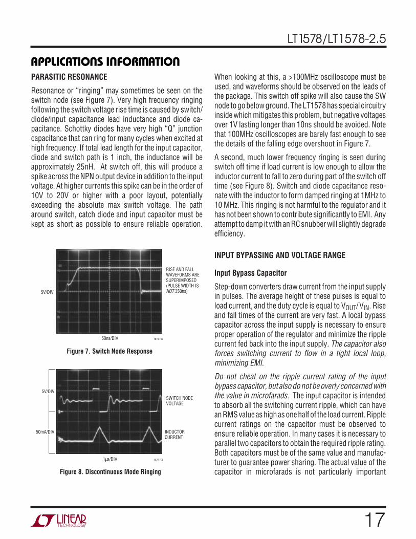
PARASITIC RESONANCE
Resonance or “ringing” may sometimes be seen on theswitch node (see Figure 7). Very high frequency ringingfollowing the switch voltage rise time is caused by switch/diode/input capacitance lead inductance and diode ca-pacitance. Schottky diodes have very high “Q” junctioncapacitance that can ring for many cycles when excited athigh frequency. If total lead length for the input capacitor,diode and switch path is 1 inch, the inductance will beapproximately 25nH. At switch off, this will produce aspike across the NPN output device in addition to the inputvoltage. At higher currents this spike can be in the order of10V to 20V or higher with a poor layout, potentiallyexceeding the absolute max switch voltage. The patharound switch, catch diode and input capacitor must bekept as short as possible to ensure reliable operation.
When looking at this, a >100MHz oscilloscope must beused, and waveforms should be observed on the leads ofthe package. This switch off spike will also cause the SWnode to go below ground. The LT1578 has special circuitryinside which mitigates this problem, but negative voltagesover 1V lasting longer than 10ns should be avoided. Notethat 100MHz oscilloscopes are barely fast enough to seethe details of the falling edge overshoot in Figure 7.
A second, much lower frequency ringing is seen duringswitch off time if load current is low enough to allow theinductor current to fall to zero during part of the switch offtime (see Figure 8). Switch and diode capacitance reso-nate with the inductor to form damped ringing at 1MHz to10 MHz. This ringing is not harmful to the regulator and ithas not been shown to contribute significantly to EMI. Anyattempt to damp it with an RC snubber will slightly degradeefficiency.
INPUT BYPASSING AND VOLTAGE RANGE
Input Bypass Capacitor
Step-down converters draw current from the input supplyin pulses. The average height of these pulses is equal toload current, and the duty cycle is equal to VOUT/VIN. Riseand fall times of the current are very fast. A local bypasscapacitor across the input supply is necessary to ensureproper operation of the regulator and minimize the ripplecurrent fed back into the input supply. The capacitor alsoforces switching current to flow in a tight local loop,minimizing EMI.
Do not cheat on the ripple current rating of the inputbypass capacitor, but also do not be overly concerned withthe value in microfarads. The input capacitor is intendedto absorb all the switching current ripple, which can havean RMS value as high as one half of the load current. Ripplecurrent ratings on the capacitor must be observed toensure reliable operation. In many cases it is necessary toparallel two capacitors to obtain the required ripple rating.Both capacitors must be of the same value and manufac-turer to guarantee power sharing. The actual value of thecapacitor in microfarads is not particularly important
Figure 7. Switch Node Response
Figure 8. Discontinuous Mode Ringing
5V/DIV
50mA/DIV
50ns/DIV 1578 F07
1µs/DIV 1578 F08
INDUCTORCURRENT
SWITCH NODEVOLTAGE
RISE AND FALLWAVEFORMS ARESUPERIMPOSED(PULSE WIDTH ISNOT 350ns)5V/DIV
18
LT1578/LT1578-2.5
APPLICATIONS INFORMATION
WU UU
because at 200kHz, any value above 15µF is essentiallyresistive. RMS ripple current rating is the critical param-eter. Actual RMS current can be calculated from:
I I V V V VRIPPLE RMS OUT OUT IN OUT IN( ) = −( )/ 2
The term inside the radical has a maximum value of 0.5when input voltage is twice output, and stays near 0.5 fora relatively wide range of input voltages. It is commonpractice therefore to simply use the worst-case value andassume that RMS ripple current is one half of load current.At maximum output current of 1.5A for the LT1578, theinput bypass capacitor should be rated at 0.75A ripplecurrent. Note however, that there are many secondaryconsiderations in choosing the final ripple current rating.These include ambient temperature, average versus peakload current, equipment operating schedule, and requiredproduct lifetime. For more details, see Application Notes19 and 46, and Design Note 95.
Input Capacitor Type
Some caution must be used when selecting the type ofcapacitor used at the input to regulators. Aluminumelectrolytics are lowest cost, but are physically large toachieve adequate ripple current rating, and size con-straints (especially height) may preclude their use.Ceramic capacitors are now available in larger values, andtheir high ripple current and voltage rating make themideal for input bypassing. Cost is fairly high and footprintmay also be somewhat large. Solid tantalum capacitorswould be a good choice, except that they have a history ofoccasional spectacular failures when they are subjected tolarge current surges during power-up. The capacitors canshort and then burn with a brilliant white light and lots ofnasty smoke. This phenomenon occurs in only a smallpercentage of units, but it has led some OEMs to forbidtheir use in high surge applications. The input bypasscapacitors of regulators can see these high surges whena battery or high capacitance source is connected. Severalmanufacturers have developed a line of solid tantalumcapacitors specially tested for surge capability (AVX TPS
series for instance, see Table 3), but even these units mayfail if the input voltage surge approaches the maximumvoltage rating of the capacitor. AVX recommends deratingcapacitor voltage by 2:1 for high surge applications. Thehighest voltage rating is 50V, so 25V may be a practicalinput voltage upper limit when using solid tantalum ca-pacitors for input bypassing.
Larger capacitors may be necessary when the input volt-age is very close to the minimum specified on the datasheet. Small voltage dips during switch on time are notnormally a problem, but at very low input voltage they maycause erratic operation because the input voltage dropsbelow the minimum specification. Problems can alsooccur if the input-to-output voltage differential is nearminimum. The amplitude of these dips is normally afunction of capacitor ESR and ESL because the capacitivereactance is small compared to these terms. ESR tends tobe the dominate term and is inversely related to physicalcapacitor size within a given capacitor type.
SYNCHRONIZING
The SYNC pin is used to synchronize the internal oscillatorto an external signal. The SYNC input must pass from alogic level low, through the maximum synchronizationthreshold with a duty cycle between 10% and 90%. Theinput can be driven directly from a logic level output. Thesynchronizing range is equal to initial operating frequencyup to 400kHz. This means that minimum practical syncfrequency is equal to the worst-case high self-oscillatingfrequency (250kHz), not the typical operating frequency of200kHz. Caution should be used when synchronizingabove 280kHz because at higher sync frequencies theamplitude of the internal slope compensation used toprevent subharmonic switching is reduced. This type ofsubharmonic switching only occurs at input voltages lessthan twice output voltage. Higher inductor values will tendto eliminate this problem. See Frequency Compensationsection for a discussion of an entirely different cause ofsubharmonic switching before assuming that the cause isinsufficient slope compensation. Application Note 19 hasmore details on the theory of slope compensation.
19
LT1578/LT1578-2.5
APPLICATIONS INFORMATION
WU UU
At power-up, when VC is being clamped by the FB pin (seeFigure 2, Q2), the sync function is disabled. This allows thefrequency foldback to operate in the shorted output con-dition. During normal operation, switching frequency iscontrolled by the internal oscillator until the FB pin reaches0.7V, after which the SYNC pin becomes operational. If nosynchronization is required, this pin should be connectedto ground.
THERMAL CALCULATIONS
Power dissipation in the LT1578 chip comes from foursources: switch DC loss, switch AC loss, boost circuitcurrent, and input quiescent current. The following formu-las show how to calculate each of these losses. Theseformulas assume continuous mode operation, so theyshould not be used for calculating efficiency at light loadcurrents.
Switch loss:
PR I V
Vns I V fSW
SW OUT OUT
INOUT IN=
( ) ( )+ ( )( )( )
2
60
Boost current loss:
PV I
VBOOSTOUT OUT
IN=
( )250/
Quiescent current loss:
P V V
V
V
Q IN OUT
OUT
IN
=
+
+
( )
− −0 55 10 1 6 10
0 004
3 3
2
. • . •
.
RSW = Switch resistance (≈0.2Ω)60ns = Equivalent switch current/voltage overlap timef = Switch frequencyExample: with VIN = 10V, VOUT = 5V and IOUT = 1A:
P
W
P W
P
SW
BOOST
Q
=( )( ) ( )
+
( )( )
= + =
=( ) ( )
=
=
+
+
( ) ( )=
−
− −
0 2 1 5
1060 10 1 10 200 10
01 012 0 22
5 1 50
100 05
10 0 55 10 5 1 6 105 0 004
100
29 3
2
3 32
.• •
. . .
/.
. • . •.
..02W
Total power dissipation is 0.22 + 0.05 + 0.02 = 0.29W.
Thermal resistance for LT1578 package is influenced bythe presence of internal or backside planes. With a fullplane under the SO package, thermal resistance will beabout 80°C/W. No plane will increase resistance to about120°C/W. To calculate die temperature, add in worst-caseambient temperature:
TJ = TA + θJA (PTOT)
With the SO-8 package (θJA = 80°C/W), at an ambienttemperature of 50°C,
TJ = 50 + 80 (0.29) = 73.2°C
Die temperature is highest at low input voltage, so uselowest continuous input operating voltage for thermalcalculations.
FREQUENCY COMPENSATION
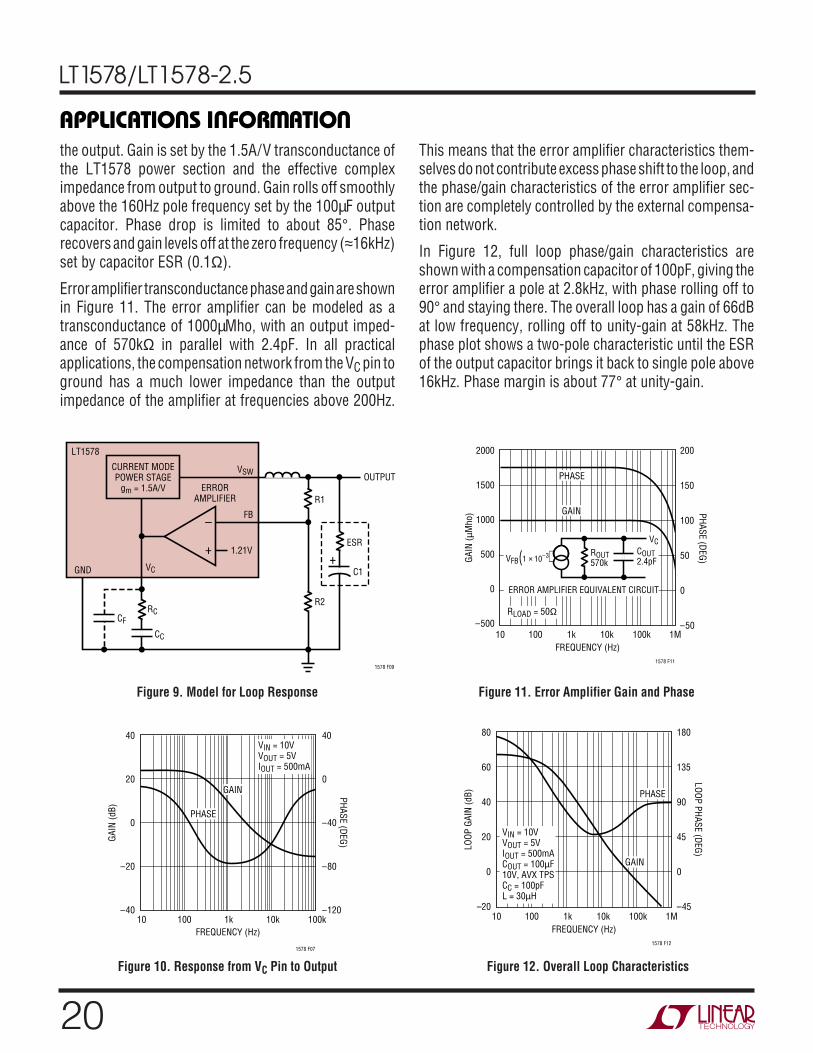
Loop frequency compensation of switching regulatorscan be a rather complicated problem because the reactivecomponents used to achieve high efficiency also intro-duce multiple poles into the feedback loop. The inductorand output capacitor on a conventional step-down con-verter actually form a resonant tank circuit that can exhibitpeaking and a rapid 180° phase shift at the resonantfrequency. By contrast, the LT1578 uses a “current mode”architecture to help alleviate the phase shift created by theinductor. The basic connections are shown in Figure 9.Figure 10 shows a Bode plot of the phase and gain of thepower section of the LT1578, measured from the VC pin to
20
LT1578/LT1578-2.5
APPLICATIONS INFORMATION
WU UU
the output. Gain is set by the 1.5A/V transconductance ofthe LT1578 power section and the effective compleximpedance from output to ground. Gain rolls off smoothlyabove the 160Hz pole frequency set by the 100µF outputcapacitor. Phase drop is limited to about 85°. Phaserecovers and gain levels off at the zero frequency (≈16kHz)set by capacitor ESR (0.1Ω).
Error amplifier transconductance phase and gain are shownin Figure 11. The error amplifier can be modeled as atransconductance of 1000µMho, with an output imped-ance of 570kΩ in parallel with 2.4pF. In all practicalapplications, the compensation network from the VC pin toground has a much lower impedance than the outputimpedance of the amplifier at frequencies above 200Hz.
This means that the error amplifier characteristics them-selves do not contribute excess phase shift to the loop, andthe phase/gain characteristics of the error amplifier sec-tion are completely controlled by the external compensa-tion network.
In Figure 12, full loop phase/gain characteristics areshown with a compensation capacitor of 100pF, giving theerror amplifier a pole at 2.8kHz, with phase rolling off to90° and staying there. The overall loop has a gain of 66dBat low frequency, rolling off to unity-gain at 58kHz. Thephase plot shows a two-pole characteristic until the ESRof the output capacitor brings it back to single pole above16kHz. Phase margin is about 77° at unity-gain.
FREQUENCY (Hz)
GAIN
(µM
ho) PHASE (DEG)
2000
1500
1000
500
0
–500
200
150
100
50
0
–5010 1k 10k 1M
1578 F11
100 100k
GAIN
PHASE
ROUT570k
COUT2.4pF
VC
ERROR AMPLIFIER EQUIVALENT CIRCUIT
RLOAD = 50Ω
VFB 1 × 10⁻³)(
–
+
1.21V
VSW
VC
LT1578
GND
1578 F09
R1
OUTPUT
ESR
CF
CC
RC
ERRORAMPLIFIER
FB
R2
C1
CURRENT MODEPOWER STAGE
gm = 1.5A/V
+
Figure 10. Response from VC Pin to Output
FREQUENCY (Hz)10
GAIN
(dB)
PHASE (DEG)
40
20
0
–20
–40
40
0
–40
–80
–120100 1k
1578 F07
10k 100k
GAIN
PHASE
VIN = 10VVOUT = 5VIOUT = 500mA
Figure 12. Overall Loop Characteristics
FREQUENCY (Hz)
LOOP
GAI
N (d
B)
LOOP PHASE (DEG)
80
60
40
20
0
–20
180
135
90
45
0
–4510 1k 10k 1M
1578 F12
100 100k
VIN = 10VVOUT = 5VIOUT = 500mACOUT = 100µF10V, AVX TPSCC = 100pFL = 30µH
PHASE
GAIN
Figure 9. Model for Loop Response Figure 11. Error Amplifier Gain and Phase
21
LT1578/LT1578-2.5
APPLICATIONS INFORMATION
WU UU
Analog experts will note that around 7kHz, phase dipsclose to the zero phase margin line. This is typical ofswitching regulators, especially those that operate over awide range of loads. This region of low phase is not aproblem as long as it does not occur near unity-gain. Inpractice, the variability of output capacitor ESR tends todominate all other effects with respect to loop response.Variations in ESR will cause unity-gain to move around,but at the same time phase moves with it so that adequatephase margin is maintained over a very wide range of ESR(≥ ±3:1).
What About a Resistor in the Compensation Network?
It is common practice in switching regulator design to adda “zero” to the error amplifier compensation to increaseloop phase margin. This zero is created in the externalnetwork in the form of a resistor (RC) in series with thecompensation capacitor. Increasing the size of this resis-tor generally creates better and better loop stability, butthere are two limitations on its value. First, the combina-tion of output capacitor ESR and a large value for RC maycause loop gain to stop rolling off altogether, creating again margin problem. An approximate formula for RCwhere gain margin falls to zero is:
R LoopV
G G ESRC
OUT
MP MA Gain = 1( ) = ( )( )( )( )1 21.
GMP = Transconductance of power stage = 1.5A/VGMA = Error amplifier transconductance = 1(10–3)ESR = Output capacitor ESR1.21 = Reference voltage
With VOUT = 5V and ESR = 0.1Ω, a value of 27.5k for RCwould yield zero gain margin, so this represents an upperlimit. There is a second limitation however which hasnothing to do with theoretical small signal dynamics. Thisresistor sets high frequency gain of the error amplifier,including the gain at the switching frequency. If theswitching frequency gain is high enough, an excessiveamout of output ripple voltage will appear at the VC pinresulting in improper operation of the regulator. In amarginal case, subharmonic switching occurs, as
evidenced by alternating pulse widths seen at the switchnode. In more severe cases, the regulator squeals orhisses audibly even though the output voltage is stillroughly correct. None of this will show on a Bode plotsince this is an amplitude insensitive measurement. Testshave shown that if ripple voltage on the VC is held to lessthan 100mVP-P, the LT1578 will generally be well behaved.The formula below will give an estimate of VC ripplevoltage when RC is added to the loop, assuming that RC islarge compared to the reactance of CC at 200kHz.
VR G V V ESR
V L fC RIPPLE
C MA IN OUT
IN( ) =
( )( ) −( )( )( )( )( )( )
1 21.
GMA = Error amplifier transconductance (1000µMho)
If a series compensation resistor of 15k gave the bestoverall loop response, with adequate gain margin, theresulting VC pin ripple voltage with VIN = 10V, VOUT = 5V,ESR = 0.1Ω, L = 30µH, would be:
Vk
VC RIPPLE( )−
−=
( )( ) −( )( )( )( )( )( ) =
15 1 10 10 5 0 1 1 21
10 30 10 200 100 151
3
6 3
• . .
• •.
This ripple voltage is high enough to possibly createsubharmonic switching. In most situations a compromisevalue (<10k in this case) for the resistor gives acceptablephase margin and no subharmonic problems. In othercases, the resistor may have to be larger to get acceptablephase response, and some means must be used to controlripple voltage at the VC pin. The suggested way to do thisis to add a capacitor (CF) in parallel with the RC/CC networkon the VC pin. The pole frequency for this capacitor istypically set at one-fifth of the switching frequency so thatit provides significant attenuation of the switching ripple,but does not add unacceptable phase shift at the loopunity-gain frequency. With RC = 15k,
Cf R k
pFFC
= ( )( )( ) = ( )( )=5
2
5
2 200 10 15265
3π π •
22
LT1578/LT1578-2.5
APPLICATIONS INFORMATION
WU UU
One way to check switching regulator loop stability is bypulse loading the regulator output while observing thetransient response at the output, using the circuit shownin Figure 13. The regulator loop is “hit” with a smalltransient AC load current at a relatively low frequency,50Hz to 1kHz. This causes the output to jump a fewmillivolts, then settle back to the original value, as shownin Figure 14. A well behaved loop will settle back cleanly,whereas a loop with poor phase or gain margin will “ring”as it settles. The number of rings indicates the degree ofstability, and the frequency of the ringing shows theapproximate unity-gain frequency of the loop. Amplitudeof the signal is not particularly important, as long as theamplitude is not so high that the loop behaves nonlinearly.
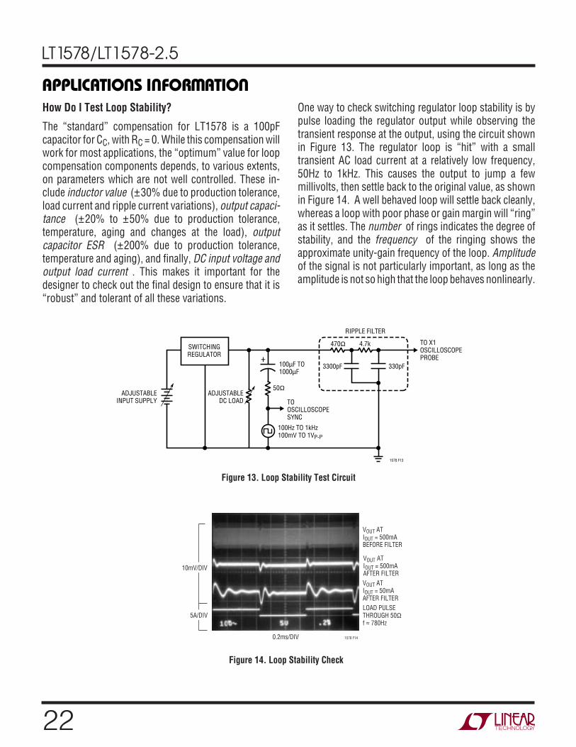
How Do I Test Loop Stability?
The “standard” compensation for LT1578 is a 100pFcapacitor for CC, with RC = 0. While this compensation willwork for most applications, the “optimum” value for loopcompensation components depends, to various extents,on parameters which are not well controlled. These in-clude inductor value (±30% due to production tolerance,load current and ripple current variations), output capaci-tance (±20% to ±50% due to production tolerance,temperature, aging and changes at the load), outputcapacitor ESR (±200% due to production tolerance,temperature and aging), and finally, DC input voltage andoutput load current . This makes it important for thedesigner to check out the final design to ensure that it is“robust” and tolerant of all these variations.
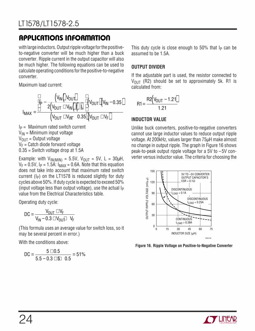
0.2ms/DIV 1578 F14
10mV/DIV
VOUT ATIOUT = 500mABEFORE FILTER
VOUT ATIOUT = 500mAAFTER FILTER
LOAD PULSETHROUGH 50Ωf ≈ 780Hz
5A/DIV
VOUT ATIOUT = 50mAAFTER FILTER
Figure 14. Loop Stability Check
TO OSCILLOSCOPESYNC
ADJUSTABLEDC LOAD
ADJUSTABLEINPUT SUPPLY
100Hz TO 1kHz100mV TO 1VP-P
100µF TO1000µF
RIPPLE FILTER
1578 F13
TO X1OSCILLOSCOPEPROBE
3300pF 330pF
50Ω
470Ω 4.7kSWITCHINGREGULATOR +
Figure 13. Loop Stability Test Circuit

23
LT1578/LT1578-2.5
APPLICATIONS INFORMATION
WU UU
The output of the regulator contains both the desired lowfrequency transient information and a reasonable amountof high frequency (200kHz) ripple. The ripple makes itdifficult to observe the small transient, so a two-pole,100kHz filter has been added. This filter is not particularlycritical; even if it attenuated the transient signal slightly,this wouldn’t matter because amplitude is not critical.
After verifying that the setup is working correctly, startvarying load current and input voltage to see if you can findany combination that makes the transient response looksuspiciously “ringy.” This procedure may lead to an ad-justment for best loop stability or faster loop transientresponse. Nearly always you will find that loop responselooks better if you add in several kΩ for RC. Do this onlyif necessary, because as explained before, RC above 1kmay require the addition of CF to control VC pin ripple.If everything looks OK, use a heat gun and cold spray onthe circuit (especially the output capacitor) to bring outany temperature-dependent characteristics.
Keep in mind that this procedure does not take initialcomponent tolerance into account. You should see fairlyclean response under all load and line conditions to ensurethat component variations will not cause problems. Onenote here: according to Murphy, the component mostlikely to be changed in production is the output capacitor,because that is the component most likely to have manu-facturer variations (in ESR) large enough to cause prob-lems. It would be a wise move to lock down the sources ofthe output capacitor in production. Also, try varying com-ponent values by a factor of 2 and see if the behavior is stillacceptable. Double and halve the values of RC and CC andoutput capacitors. If the regulator still works correctly, itwill likely be good in production.
A possible exception to the “clean response” rule is at verylight loads, as evidenced in Figure 14 with ILOAD = 50mA.Switching regulators tend to have dramatic shifts in loopresponse at very light loads, mostly because the inductorcurrent becomes discontinuous. One common result is veryslow but stable characteristics. A second possibility is lowphase margin, as evidenced by ringing at the output withtransients. The good news is that the low phase margin at
light loads is not particularly sensitive to component varia-tion, so if it looks reasonable under a transient test, it willprobably not be a problem in production. Note that fre-quency of the light load ringing may vary with componenttolerance but phase margin generally hangs in there.
POSITIVE-TO-NEGATIVE CONVERTER
The circuit in Figure 15 is a classic positive-to-negativetopology using a grounded inductor. It differs from thestandard approach in the way the IC chip derives itsfeedback signal. Because the LT1578 accepts only posi-tive feedback signals, the ground pin must be tied to theregulated negative output. A resistor divider to ground or,in this case, the sense pin, then provides the properfeedback voltage for the chip.
Figure 15. Positive-to-Negative Converter
OUTPUT**–5V, 0.5A
INPUT5.5V TO
15V
1578 F15
C20.33µF
CC
RC
D21N5818
C1100µF10V TANT×2
R115.8k
R24.99k
C310µF TO
50µF
D11N4148
L1*15µHBOOST
LT1578
VIN VSW
FBGND VC
* INCREASE L1 TO 30µH OR 60µH FOR HIGHER CURRENT APPLICATIONS. SEE APPLICATIONS INFORMATION
** MAXIMUM LOAD CURRENT DEPENDS ON MINIMUM INPUT VOLTAGE AND INDUCTOR SIZE. SEE APPLICATIONS INFORMATION
++
Inverting regulators differ from buck regulators in thebasic switching network. Current is delivered to the outputas square waves with a peak-to-peak amplitude muchgreater than load current. This means that maximum loadcurrent will be significantly less than the LT1578’s 1.5Amaximum switch current, even with large inductor values.The buck converter in comparison, delivers current to theoutput as a triangular wave superimposed on a DC levelequal to load current, and load current can approach 1.5A
24
LT1578/LT1578-2.5
APPLICATIONS INFORMATION
WU UU
with large inductors. Output ripple voltage for the positive-to-negative converter will be much higher than a buckconverter. Ripple current in the output capacitor will alsobe much higher. The following equations can be used tocalculate operating conditions for the positive-to-negativeconverter.
Maximum load current:
I
IV V
V V f LV V
V V V VMAX
PIN OUT
OUT INOUT IN
OUT IN OUT F=
−( )( )
+( )( )( )
( ) −( )
+ −( ) +( )2
0 35
0 35
.
.
IP = Maximum rated switch currentVIN = Minimum input voltageVOUT = Output voltageVF = Catch diode forward voltage0.35 = Switch voltage drop at 1.5A
Example: with VIN(MIN) = 5.5V, VOUT = 5V, L = 30µH,VF = 0.5V, IP = 1.5A: IMAX = 0.6A. Note that this equationdoes not take into account that maximum rated switchcurrent (IP) on the LT1578 is reduced slightly for dutycycles above 50%. If duty cycle is expected to exceed 50%(input voltage less than output voltage), use the actual IPvalue from the Electrical Characteristics table.
Operating duty cycle:
DCV V
V V VOUT F
IN OUT F= +
− + +0 3.
(This formula uses an average value for switch loss, so itmay be several percent in error.)
With the conditions above:
DC = +− + +
=5 0 55 5 0 3 5 0 5
51.
. . .%
This duty cycle is close enough to 50% that IP can beassumed to be 1.5A.
OUTPUT DIVIDER
If the adjustable part is used, the resistor connected toVOUT (R2) should be set to approximately 5k. R1 iscalculated from:
RR VOUT
12 1 21
1 21=
−( ).
.
INDUCTOR VALUE
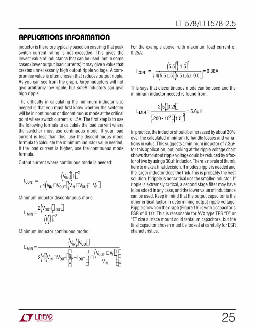
Unlike buck converters, positive-to-negative converterscannot use large inductor values to reduce output ripplevoltage. At 200kHz, values larger than 75µH make almostno change in output ripple. The graph in Figure 16 showspeak-to-peak output ripple voltage for a 5V to –5V con-verter versus inductor value. The criteria for choosing the
INDUCTOR SIZE (µH)0
OUTP
UT R
IPPL
E VO
LTAG
E (m
V P-P
)
150
120
90
60
30
060
1578 F16
15 30 45 75
DISCONTINUOUSILOAD = 0.25A
DISCONTINUOUSILOAD = 0.1A
5V TO –5V CONVERTEROUTPUT CAPACITOR’SESR = 0.1Ω
CONTINUOUSILOAD > 0.38A
Figure 16. Ripple Voltage on Positive-to-Negative Converter
25
LT1578/LT1578-2.5
APPLICATIONS INFORMATION
WU UU
For the example above, with maximum load current of0.25A:
I ACONT =( ) ( )+( ) + +( ) =5 5 1 5
4 5 5 5 5 5 5 0 50 38
2 2. .
. . ..
This says that discontinuous mode can be used and theminimum inductor needed is found from:
L HMIN =( )( )
( )
=2 5 0 25
200 10 1 55 6
3 2
.
• .. µ
In practice, the inductor should be increased by about 30%over the calculated minimum to handle losses and varia-tions in value. This suggests a minimum inductor of 7.3µHfor this application, but looking at the ripple voltage chartshows that output ripple voltage could be reduced by a fac-tor of two by using a 30µH inductor. There is no rule of thumbhere to make a final decision. If modest ripple is needed andthe larger inductor does the trick, this is probably the bestsolution. If ripple is noncritical use the smaller inductor. Ifripple is extremely critical, a second stage filter may haveto be added in any case, and the lower value of inductancecan be used. Keep in mind that the output capacitor is theother critical factor in determining output ripple voltage.Ripple shown on the graph (Figure 16) is with a capacitor’sESR of 0.1Ω. This is reasonable for AVX type TPS “D” or“E” size surface mount solid tantalum capacitors, but thefinal capacitor chosen must be looked at carefully for ESRcharacteristics.
inductor is therefore typically based on ensuring that peakswitch current rating is not exceeded. This gives thelowest value of inductance that can be used, but in somecases (lower output load currents) it may give a value thatcreates unnecessarily high output ripple voltage. A com-promise value is often chosen that reduces output ripple.As you can see from the graph, large inductors will notgive arbitrarily low ripple, but small inductors can givehigh ripple.
The difficulty in calculating the minimum inductor sizeneeded is that you must first know whether the switcherwill be in continuous or discontinuous mode at the criticalpoint where switch current is 1.5A. The first step is to usethe following formula to calculate the load current wherethe switcher must use continuous mode. If your loadcurrent is less than this, use the discontinuous modeformula to calculate the minimum inductor value needed.If the load current is higher, use the continuous modeformula.
Output current where continuous mode is needed:
IV I
V V V V VCONT
IN P
IN OUT IN OUT F
=( ) ( )
+( ) + +( )2 2
4
Minimum inductor discontinuous mode:
LV I
f IMIN
OUT OUT
P
=( )( )
( )( )2
2
Minimum inductor continuous mode:
LV V
f V V I IV V
V
MININ OUT
IN OUT P OUTOUT F
IN
=( )( )
( ) +( ) − ++( )
2 1
26
LT1578/LT1578-2.5
Ripple Current in the Input and Output Capacitors
Positive-to-negative converters have high ripple current inboth the input and output capacitors. For long capacitorlifetime, the RMS value of this current must be less thanthe high frequency ripple current rating of the capacitor.The following formula will give an approximate value forRMS ripple current. This formula assumes continuousconduction mode and a large inductor value. Small induc-tors will give somewhat higher ripple current, especially indiscontinuous mode. The exact formulas are very com-plex and appear in Application Note 44, pages 30 and 31.For our purposes here, a simple fudge factor (ff) is added.The value for ff is about 1.2 for load currents above 0.38A(in continuous conduction mode) and L ≥10µH. It in-creases to about 2.0 for smaller inductors at lower loadcurrents (in discontinuous conduction mode).
Capacitor ff IVVOUTOUT
IN IRMS = ( )( )
ff = Fudge factor (1.2 to 2.0)
APPLICATIONS INFORMATION
WU UU
Diode Current
Average diode current is equal to load current. Peak diodecurrent will be considerably higher.
Peak diode current:
Continuous
IV V
V
V V
L f V V
DiscontinuousV
L f
OUTIN OUT
IN
IN OUT
IN OUT
OUT
Mode
Mode =2 IOUT
=+( )
+( )( )
( )( ) +( )
( )( )( )( )
2
Keep in mind that during start-up and output overloads,the average diode current may be much higher than withnormal loads. Care should be used if diodes rated less than1A are used, especially if continuous overload conditionsmust be tolerated.
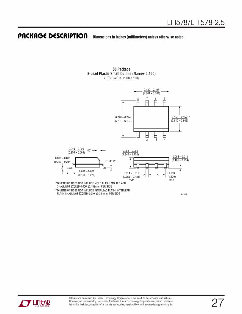
27
LT1578/LT1578-2.5
Dimensions in inches (millimeters) unless otherwise noted.PACKAGE DESCRIPTION
U
S8 Package8-Lead Plastic Small Outline (Narrow 0.150)
(LTC DWG # 05-08-1610)
0.016 – 0.050(0.406 – 1.270)
0.010 – 0.020(0.254 – 0.508)
× 45°
0°– 8° TYP0.008 – 0.010
(0.203 – 0.254)
SO8 1298
0.053 – 0.069(1.346 – 1.752)
0.014 – 0.019(0.355 – 0.483)
TYP
0.004 – 0.010(0.101 – 0.254)
0.050(1.270)
BSC
1 2 3 4
0.150 – 0.157**(3.810 – 3.988)
8 7 6 5
0.189 – 0.197*(4.801 – 5.004)
0.228 – 0.244(5.791 – 6.197)
DIMENSION DOES NOT INCLUDE MOLD FLASH. MOLD FLASH SHALL NOT EXCEED 0.006" (0.152mm) PER SIDEDIMENSION DOES NOT INCLUDE INTERLEAD FLASH. INTERLEAD FLASH SHALL NOT EXCEED 0.010" (0.254mm) PER SIDE
*
**
Information furnished by Linear Technology Corporation is believed to be accurate and reliable.However, no responsibility is assumed for its use. Linear Technology Corporation makes no represen-tation that the interconnection of its circuits as described herein will not infringe on existing patent rights.
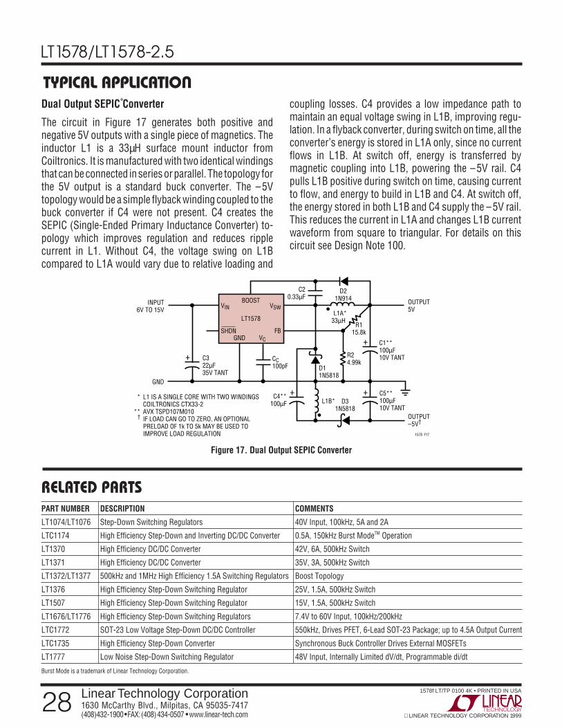
28
LT1578/LT1578-2.5
PART NUMBER DESCRIPTION COMMENTS
LT1074/LT1076 Step-Down Switching Regulators 40V Input, 100kHz, 5A and 2A
LTC1174 High Efficiency Step-Down and Inverting DC/DC Converter 0.5A, 150kHz Burst ModeTM Operation
LT1370 High Efficiency DC/DC Converter 42V, 6A, 500kHz Switch
LT1371 High Efficiency DC/DC Converter 35V, 3A, 500kHz Switch
LT1372/LT1377 500kHz and 1MHz High Efficiency 1.5A Switching Regulators Boost Topology
LT1376 High Efficiency Step-Down Switching Regulator 25V, 1.5A, 500kHz Switch
LT1507 High Efficiency Step-Down Switching Regulator 15V, 1.5A, 500kHz Switch
LT1676/LT1776 High Efficiency Step-Down Switching Regulators 7.4V to 60V Input, 100kHz/200kHz
LTC1772 SOT-23 Low Voltage Step-Down DC/DC Controller 550kHz, Drives PFET, 6-Lead SOT-23 Package; up to 4.5A Output Current
LTC1735 High Efficiency Step-Down Converter Synchronous Buck Controller Drives External MOSFETs
LT1777 Low Noise Step-Down Switching Regulator 48V Input, Internally Limited dV/dt, Programmable di/dt
Burst Mode is a trademark of Linear Technology Corporation.
1578f LT/TP 0100 4K • PRINTED IN USA
LINEAR TECHNOLOGY CORPORATION 1999
TYPICAL APPLICATION
U
Dual Output SEPIC Converter
The circuit in Figure 17 generates both positive andnegative 5V outputs with a single piece of magnetics. Theinductor L1 is a 33µH surface mount inductor fromCoiltronics. It is manufactured with two identical windingsthat can be connected in series or parallel. The topology forthe 5V output is a standard buck converter. The –5Vtopology would be a simple flyback winding coupled to thebuck converter if C4 were not present. C4 creates theSEPIC (Single-Ended Primary Inductance Converter) to-pology which improves regulation and reduces ripplecurrent in L1. Without C4, the voltage swing on L1Bcompared to L1A would vary due to relative loading and
Linear Technology Corporation1630 McCarthy Blvd., Milpitas, CA 95035-7417(408) 432-1900 FAX: (408) 434-0507 www.linear-tech.com
BOOST
LT1578
VINOUTPUT5V
OUTPUT–5V†
* L1 IS A SINGLE CORE WITH TWO WINDINGSCOILTRONICS CTX33-2
** AVX TSPD107M010† IF LOAD CAN GO TO ZERO, AN OPTIONAL
PRELOAD OF 1k TO 5k MAY BE USED TOIMPROVE LOAD REGULATION
INPUT6V TO 15V
GND
1578 F17
C20.33µF
CC100pF D1
1N5818
C1**100µF10V TANT
C5**100µF10V TANT
C322µF35V TANT
C4**100µF
D21N914
R115.8k
R24.99k
D31N5818
L1A*33µH
L1B*
VSW
FBGND
SHDNVC
+
+
+
+
RELATED PARTS
Figure 17. Dual Output SEPIC Converter
coupling losses. C4 provides a low impedance path tomaintain an equal voltage swing in L1B, improving regu-lation. In a flyback converter, during switch on time, all theconverter’s energy is stored in L1A only, since no currentflows in L1B. At switch off, energy is transferred bymagnetic coupling into L1B, powering the –5V rail. C4pulls L1B positive during switch on time, causing currentto flow, and energy to build in L1B and C4. At switch off,the energy stored in both L1B and C4 supply the –5V rail.This reduces the current in L1A and changes L1B currentwaveform from square to triangular. For details on thiscircuit see Design Note 100.