
DPDT SWITCH GaAs MMIC: RF Switches · DPDT SWITCH GaAs MMIC FEATURES Low control voltage 1.8V min....
12
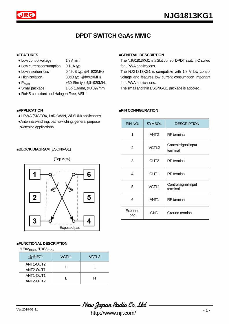
NJG1813KG1 - 1 - Ver.2019-05-31 http://www.njr.com/ DPDT SWITCH GaAs MMIC ■FEATURES ● Low control voltage 1.8V min. ● Low current consumption 0.1μA typ. ● Low insertion loss 0.45dB typ. @f=920MHz ● High isolation 30dB typ. @f=920MHz ● P -0.1dB +30dBm typ. @f=920MHz ● Small package 1.6 x 1.6mm, t=0.397mm ● RoHS compliant and Halogen Free, MSL1 ■APPLICATION ● LPWA (SIGFOX, LoRaWAN, Wi-SUN) applications ●Antenna switching, path switching, general purpose switching applications ■BLOCK DIAGRAM (ESON6-G1) ■FUNCTIONAL DESCRIPTION “H”=V CTL(H) , “L”=V CTL(L) 通過経路 VCTL1 VCTL2 ANT1-OUT2 ANT2-OUT1 H L ANT1-OUT1 ANT2-OUT2 L H ■GENERAL DESCRIPTION The NJG1813KG1 is a 2bit control DPDT switch IC suited for LPWA applications. The NJG1813KG1 is compatible with 1.8 V low control voltage and features low current consumption important for LPWA applications. The small and thin ESON6-G1 package is adopted. ■PIN CONFIGURATION PIN NO. SYMBOL DESCRIPTION 1 ANT2 RF terminal 2 VCTL2 Control signal input terminal 3 OUT2 RF terminal 4 OUT1 RF terminal 5 VCTL1 Control signal input terminal 6 ANT1 RF terminal Exposed pad GND Ground terminal (Top view) Exposed pad
Transcript of DPDT SWITCH GaAs MMIC: RF Switches · DPDT SWITCH GaAs MMIC FEATURES Low control voltage 1.8V min....
NJG1813KG1
- 1 - Ver.2019-05-31 http://www.njr.com/
DPDT SWITCH GaAs MMIC ■FEATURES ● Low control voltage 1.8V min. ● Low current consumption 0.1μA typ. ● Low insertion loss 0.45dB typ. @f=920MHz ● High isolation 30dB typ. @f=920MHz ● P-0.1dB +30dBm typ. @f=920MHz ● Small package 1.6 x 1.6mm, t=0.397mm ● RoHS compliant and Halogen Free, MSL1
■APPLICATION ● LPWA (SIGFOX, LoRaWAN, Wi-SUN) applications ●Antenna switching, path switching, general purpose switching applications
■BLOCK DIAGRAM (ESON6-G1) ■FUNCTIONAL DESCRIPTION
“H”=VCTL(H), “L”=VCTL(L)
通過経路 VCTL1 VCTL2
ANT1-OUT2 ANT2-OUT1
H L
ANT1-OUT1 ANT2-OUT2
L H
■GENERAL DESCRIPTION The NJG1813KG1 is a 2bit control DPDT switch IC suited for LPWA applications. The NJG1813KG1 is compatible with 1.8 V low control voltage and features low current consumption important for LPWA applications. The small and thin ESON6-G1 package is adopted.
■PIN CONFIGURATION
PIN NO. SYMBOL DESCRIPTION
1 ANT2 RF terminal
2 VCTL2 Control signal input terminal
3 OUT2 RF terminal
4 OUT1 RF terminal
5 VCTL1 Control signal input terminal
6 ANT1 RF terminal
Exposed pad GND Ground terminal
(Top view)
Exposed pad
NJG1813KG1
- 2 - Ver.2019-05-31 http://www.njr.com/
■ PRODUCT NAME INFORMATION ■ ORDERING INFORMATION
PART NUMBER
PACKAGE OUTLINE RoHS HALOGEN-
FREE TERMINAL
FINISH MARKING WEIGHT (mg) MOQ (pcs.)
NJG1813KG1 ESON6-G1 Yes Yes Sn-Bi 1813 3.5 3,000
■ ABSOLUTE MAXIMUM RATINGS
Ta=25°C, Zs=Zl=50
PARAMETER SYMBOL RATINGS UNIT
Control Voltage VCTL 4.5 V
RF Input Power PIN +33 dBm
Power Dissipation (1) PD 1200 mW
Operating Temperature Topr -40 to +105 °C
Storage Temperature Tstg -55 to +150 °C
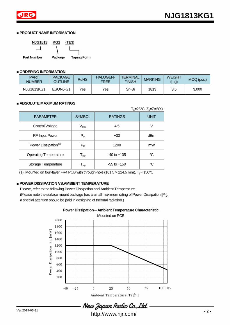
(1): Mounted on four-layer FR4 PCB with through-hole (101.5 × 114.5 mm), Tj = 150°C ■ POWER DISSIPATION VS.AMBIENT TEMPERATURE
Please, refer to the following Power Dissipation and Ambient Temperature. (Please note the surface mount package has a small maximum rating of Power Dissipation [PD], a special attention should be paid in designing of thermal radiation.)
NJG1813 KG1 (TE3)
Part Number Taping Form Package
Power Dissipation-Ambient Temperature Characteristic Mounted on PCB
-40 -25 0 25 50 75 100 1050
200400600800
100012001400160018002000
Pow
er D
issi
patio
nP D
[mW
]
Ambient Temperature Ta[℃]
NJG1813KG1
- 3 - Ver.2019-05-31 http://www.njr.com/
■ ELECTRICAL CHARACTERISTICS (DC CHARACTERISTICS) VCTL(H)=3.0V, VCTL(L)=0V, Ta=25°C, Zs=Zl=50, with application circuit
PARAMETER SYMBOL TEST CONDITION MIN. TYP. MAX. UNIT
Control Voltage (HIGH) VCTL(H) 1.8 3.0 4.0 V
Control Voltage (LOW) VCTL(L) -0.2 - 0.2 V
Control Current ICTL RF OFF, VCTL(H)=3.0V, VCTL(L)=0V - 0.1 2.5 μA
■ ELECTRICAL CHARACTERISTICS (RF CHARACTERISTICS)
VCTL(H)=3.0V, VCTL(L)=0V, Ta=25°C, Zs=Zl=50, with application circuit
PARAMETER SYMBOL TEST CONDITION MIN. TYP. MAX. UNIT
Insertion loss LOSS f=920MHz - 0.45 0.68 dB
Isolation1 ISL1 f=920MHz, ANT1/2 to OUT1/2 26 30 - dB
Isolation2 ISL2 f=920MHz, ANT1 to ANT2, OUT1 to OUT2 26 30 - dB
Input power at 0.1dB compression point P-0.1dB f=920MHz +27 +30 - dBm
VSWR VSWR f=920MHz - 1.1 1.5 -
Switching time TSW 50% VCTL to 10%/90% RF - 100 300 ns
NJG1813KG1
- 4 - Ver.2019-05-31 http://www.njr.com/
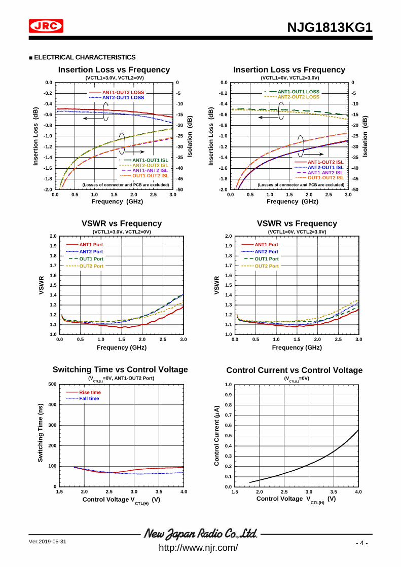
■ ELECTRICAL CHARACTERISTICS
0
100
200
300
400
500
1.5 2.0 2.5 3.0 3.5 4.0
Rise timeFall time
Switc
hing
Tim
e (n
s)
Control Voltage VCTL(H)
(V)
(VCTL(L)
=0V, ANT1-OUT2 Port)Switching Time vs Control Voltage
0.0
0.1
0.2
0.3
0.4
0.5
0.6
0.7
0.8
0.9
1.0
1.5 2.0 2.5 3.0 3.5 4.0
Control Current vs Control Voltage
Con
trol
Cur
rent
(A
)
Control Voltage VCTL(H)
(V)
(VCTL(L)
=0V)
-2.0
-1.8
-1.6
-1.4
-1.2
-1.0
-0.8
-0.6
-0.4
-0.2
0.0
-50
-45
-40
-35
-30
-25
-20
-15
-10
-5
0
0.0 0.5 1.0 1.5 2.0 2.5 3.0
ANT1-OUT2 LOSSANT2-OUT1 LOSS
ANT1-OUT1 ISLANT2-OUT2 ISLANT1-ANT2 ISLOUT1-OUT2 ISL
Inse
rtio
n Lo
ss (
dB)
Isol
atio
n (d
B)
Frequency (GHz)
(VCTL1=3.0V, VCTL2=0V)Insertion Loss vs Frequency
(Losses of connector and PCB are excluded)-2.0
-1.8
-1.6
-1.4
-1.2
-1.0
-0.8
-0.6
-0.4
-0.2
0.0
-50
-45
-40
-35
-30
-25
-20
-15
-10
-5
0
0.0 0.5 1.0 1.5 2.0 2.5 3.0
ANT1-OUT1 LOSSANT2-OUT2 LOSS
ANT1-OUT2 ISLANT2-OUT1 ISLANT1-ANT2 ISLOUT1-OUT2 ISL
Inse
rtio
n Lo
ss (
dB)
Isol
atio
n (d
B)
Frequency (GHz)
(VCTL1=0V, VCTL2=3.0V)Insertion Loss vs Frequency
(Losses of connector and PCB are excluded)
(VCTL1=3.0V, VCTL2=0V)
1.0
1.1
1.2
1.3
1.4
1.5
1.6
1.7
1.8
1.9
2.0
0.0 0.5 1.0 1.5 2.0 2.5 3.0
ANT1 PortANT2 PortOUT1 PortOUT2 Port
VSW
R
Frequency (GHz)
VSWR vs Frequency(VCTL1=0V, VCTL2=3.0V)
1.0
1.1
1.2
1.3
1.4
1.5
1.6
1.7
1.8
1.9
2.0
0.0 0.5 1.0 1.5 2.0 2.5 3.0
ANT1 PortANT2 PortOUT1 PortOUT2 Port
VSW
R
Frequency (GHz)
VSWR vs Frequency
NJG1813KG1
- 5 - Ver.2019-05-31 http://www.njr.com/
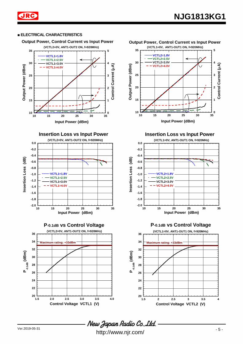
■ ELECTRICAL CHARACTERISTICS
10
15
20
25
30
35
0
1
2
3
4
5
10 15 20 25 30 35
Output Power, Control Current vs Input Power
VCTL1=1.8VVCTL1=2.5VVCTL1=3.0VVCTL1=4.0V
VCTL1=1.8VVCTL1=2.5VVCTL1=3.0VVCTL1=4.0V
Out
put P
ower
(dB
m)
Con
trol
Cur
rent
(A
)
Input Power (dBm)
(VCTL2=0V, ANT1-OUT2 ON, f=920MHz)
10
15
20
25
30
35
0
1
2
3
4
5
10 15 20 25 30 35
Output Power, Control Current vs Input Power
VCTL2=1.8VVCTL2=2.5VVCTL2=3.0VVCTL2=4.0V
VCTL2=1.8VVCTL2=2.5VVCTL2=3.0VVCTL2=4.0V
Out
put P
ower
(dB
m)
Con
trol
Cur
rent
(A
)
Input Power (dBm)
(VCTL1=0V, ANT1-OUT1 ON, f=920MHz)
-2.0
-1.8
-1.6
-1.4
-1.2
-1.0
-0.8
-0.6
-0.4
-0.2
0.0
10 15 20 25 30 35
VCTL1=1.8VVCTL1=2.5VVCTL1=3.0VVCTL1=4.0V
Inse
rtio
n Lo
ss (
dB)
Input Power (dBm)
�Insertion Loss vs Input Power(VCTL2=0V, ANT1-OUT2 ON, f=920MHz)
-2.0
-1.8
-1.6
-1.4
-1.2
-1.0
-0.8
-0.6
-0.4
-0.2
0.0
10 15 20 25 30 35
VCTL2=1.8VVCTL2=2.5VVCTL2=3.0VVCTL2=4.0V
Inse
rtio
n Lo
ss (
dB)
Input Power (dBm)
�Insertion Loss vs Input Power(VCTL1=0V, ANT1-OUT1 ON, f=920MHz)
20
22
24
26
28
30
32
34
36
1.5 2.0 2.5 3.0 3.5 4.0
P -0.1
dB (d
Bm
)
Control Voltage VCTL1 (V)
(VCTL2=0V, ANT1-OUT2 ON, f=920MHz)
P-0.1dB vs Control Voltage
Maximum rating: +33dBm
20
22
24
26
28
30
32
34
36
1.5 2 2.5 3 3.5 4
P -0.1
dB (d
Bm
)
Control Voltage VCTL2 (V)
(VCTL1=0V, ANT1-OUT1 ON, f=920MHz)
P-0.1dB vs Control Voltage
Maximum rating: +33dBm
NJG1813KG1
- 6 - Ver.2019-05-31 http://www.njr.com/
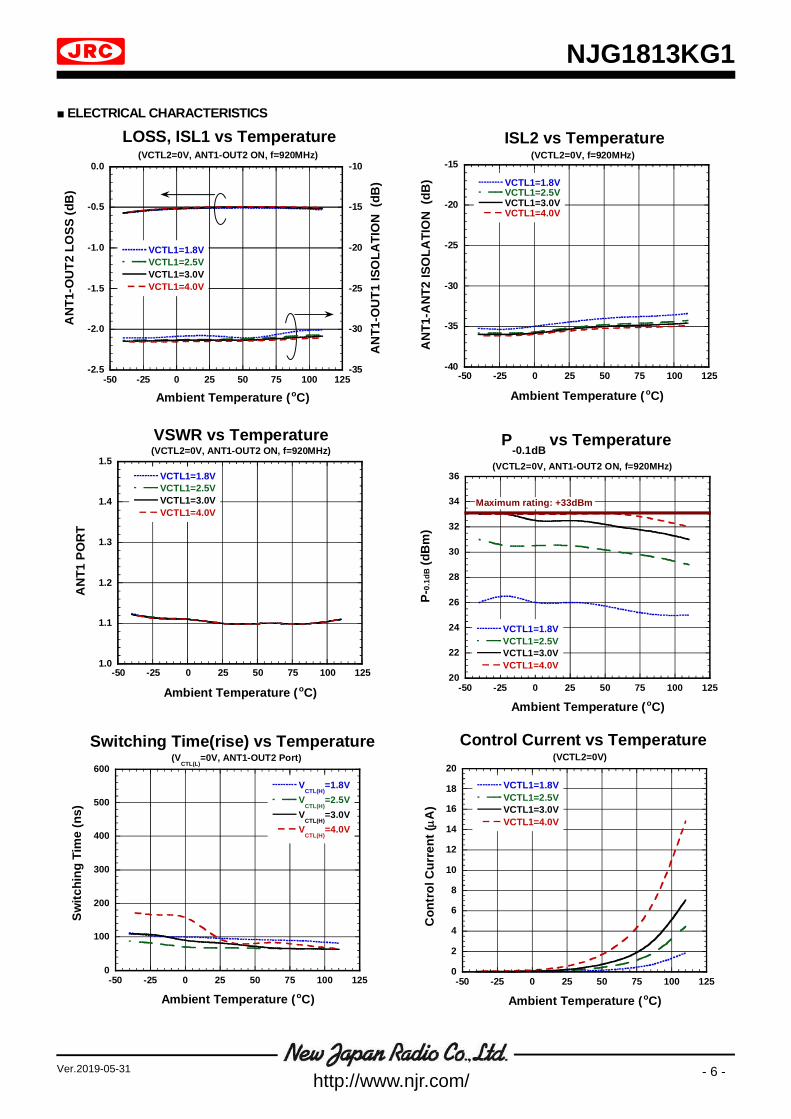
■ ELECTRICAL CHARACTERISTICS
-2.5
-2.0
-1.5
-1.0
-0.5
0.0
-35
-30
-25
-20
-15
-10
-50 -25 0 25 50 75 100 125
VCTL1=2.5VVCTL1=1.8VVCTL1=3.0VVCTL1=4.0V
VCTL1=1.8VVCTL1=2.5VVCTL1=3.0VVCTL1=4.0V
AN
T1-O
UT2
LO
SS (d
B)
AN
T1-O
UT1
ISO
LATI
ON
(dB
)
Ambient Temperature (oC)
(VCTL2=0V, ANT1-OUT2 ON, f=920MHz)LOSS, ISL1 vs Temperature
-40
-35
-30
-25
-20
-15
-50 -25 0 25 50 75 100 125
ISL2 vs Temperature
VCTL1=1.8VVCTL1=2.5VVCTL1=3.0VVCTL1=4.0V
AN
T1-A
NT2
ISO
LATI
ON
(dB
)
Ambient Temperature (oC)
(VCTL2=0V, f=920MHz)
1.0
1.1
1.2
1.3
1.4
1.5
-50 -25 0 25 50 75 100 125
VSWR vs Temperature
VCTL1=1.8VVCTL1=2.5VVCTL1=3.0VVCTL1=4.0V
AN
T1 P
OR
T
Ambient Temperature (oC)
(VCTL2=0V, ANT1-OUT2 ON, f=920MHz)
20
22
24
26
28
30
32
34
36
-50 -25 0 25 50 75 100 125
VCTL1=1.8VVCTL1=2.5VVCTL1=3.0VVCTL1=4.0V
P-0.
1dB (
dBm
)
Ambient Temperature (oC)
(VCTL2=0V, ANT1-OUT2 ON, f=920MHz)
P-0.1dB
vs Temperature
Maximum rating: +33dBm
0
100
200
300
400
500
600
-50 -25 0 25 50 75 100 125
VCTL(H)
=1.8VV
CTL(H)=2.5V
VCTL(H)
=3.0VV
CTL(H)=4.0V
Switc
hing
Tim
e (n
s)
Ambient Temperature (oC)
(VCTL(L)
=0V, ANT1-OUT2 Port)Switching Time(rise) vs Temperature
0
2
4
6
8
10
12
14
16
18
20
-50 -25 0 25 50 75 100 125
Control Current vs Temperature
VCTL1=1.8VVCTL1=2.5VVCTL1=3.0VVCTL1=4.0V
Con
trol
Cur
rent
(A
)
Ambient Temperature (oC)
(VCTL2=0V)
NJG1813KG1
- 7 - Ver.2019-05-31 http://www.njr.com/
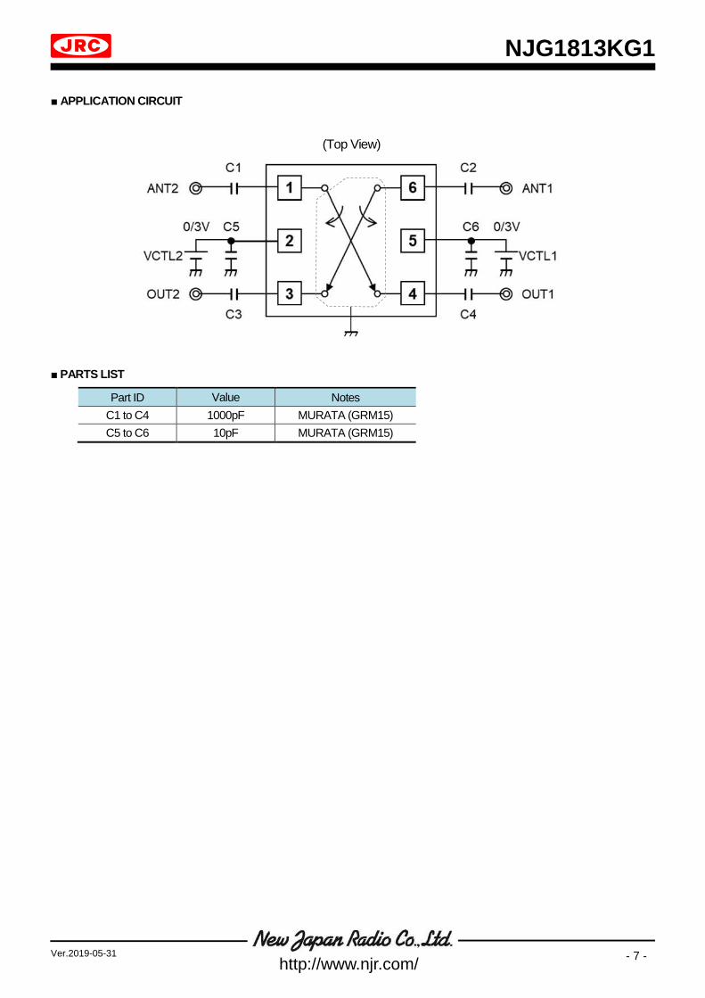
■ APPLICATION CIRCUIT ■ PARTS LIST
Part ID Value Notes C1 to C4 1000pF MURATA (GRM15) C5 to C6 10pF MURATA (GRM15)
(Top View)
NJG1813KG1
- 8 - Ver.2019-05-31 http://www.njr.com/
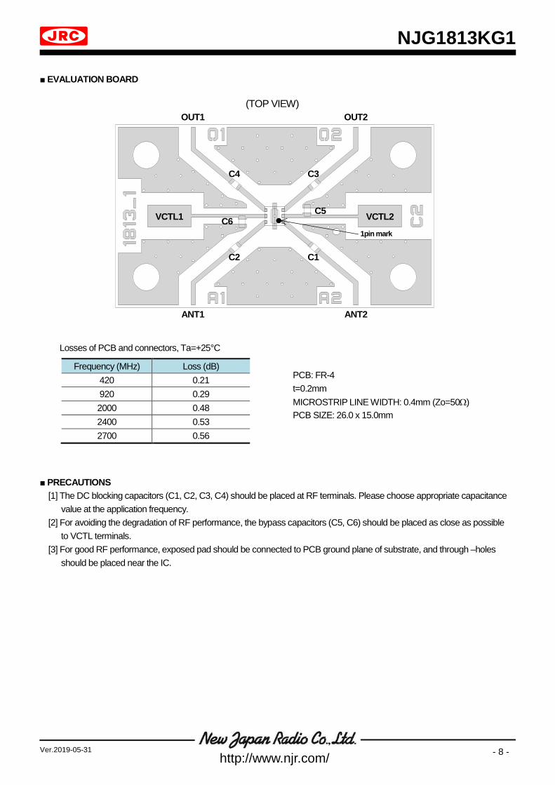
■ EVALUATION BOARD
Losses of PCB and connectors, Ta=+25°C
■ PRECAUTIONS
[1] The DC blocking capacitors (C1, C2, C3, C4) should be placed at RF terminals. Please choose appropriate capacitance value at the application frequency.
[2] For avoiding the degradation of RF performance, the bypass capacitors (C5, C6) should be placed as close as possible to VCTL terminals.
[3] For good RF performance, exposed pad should be connected to PCB ground plane of substrate, and through –holes should be placed near the IC.
Frequency (MHz) Loss (dB) 420 0.21 920 0.29 2000 0.48 2400 0.53 2700 0.56
(TOP VIEW)
ANT1 ANT2
OUT1 OUT2
VCTL1 VCTL2 1pin mark
C1 C2
C3 C4
C5 C6
PCB: FR-4 t=0.2mm MICROSTRIP LINE WIDTH: 0.4mm (Zo=50) PCB SIZE: 26.0 x 15.0mm
NJG1813KG1
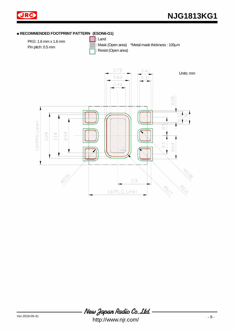
- 9 - Ver.2019-05-31 http://www.njr.com/
■ RECOMMENDED FOOTPRINT PATTERN (ESON6-G1) : Land : Mask (Open area) *Metal mask thickness : 100m : Resist (Open area)
PKG: 1.6 mm x 1.6 mm Pin pitch: 0.5 mm
Units: mm
NJG1813KG1
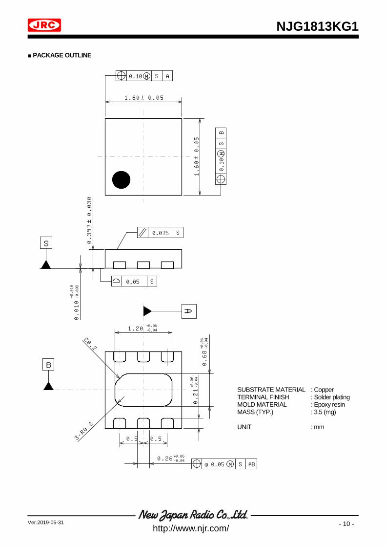
- 10 - Ver.2019-05-31 http://www.njr.com/
■ PACKAGE OUTLINE
SUBSTRATE MATERIAL : Copper TERMINAL FINISH : Solder plating MOLD MATERIAL : Epoxy resin MASS (TYP.) : 3.5 (mg) UNIT : mm
B
A
S
1.60±0.05
0.10 M S A
1.60±0.05
0.10MSB
0.075 S
0.05 S
0.397±0.030
0.010
1.20+0.06-0.04
0.5 0.5
0.26 +0.06-0.04φ0.05 M S AB
3-R0.2
C0.2
0.68+0.06
-0.04
0.21+0.06
-0.04
+0.010
-0.008
NJG1813KG1
- 11 - Ver.2019-05-31 http://www.njr.com/
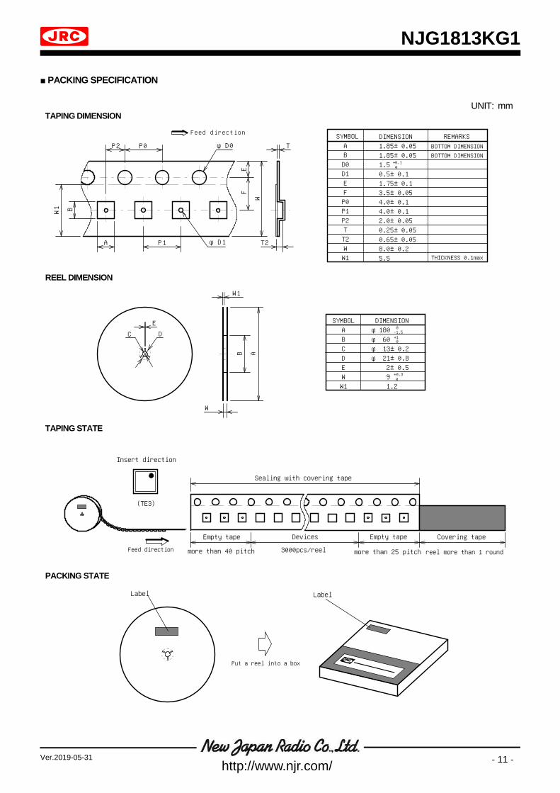
■ PACKING SPECIFICATION
UNIT: mm TAPING DIMENSION
Feed direction
A
BW1
P2 P0
P1
φD0
EF
W
T
T2φD1
SYMBOL
A
B
D0
D1
E
F
P0
P1
P2
T
T2
W
W1
DIMENSION
1.85±0.05
1.85±0.05
1.5
0.5±0.1
1.75±0.1
3.5±0.05
4.0±0.1
4.0±0.1
2.0±0.05
0.25±0.05
0.65±0.05
8.0±0.2
5.5
REMARKS
BOTTOM DIMENSION
BOTTOM DIMENSION
THICKNESS 0.1max
+0.10
REEL DIMENSION
A
E
C D
B
W1
W
SYMBOL
A
B
C
D
E
W
W1
DIMENSION
φ180
φ 60
φ 13±0.2
φ 21±0.8
2±0.5
9
1.2
0-1.5+10
0+0.3
TAPING STATE
more than 40 pitch 3000pcs/reel
Empty tape
more than 25 pitch
Covering tape
reel more than 1 round
Sealing with covering tape
Feed direction
Devices Empty tape
PACKING STATE
Insert direction
(TE3)
Label
Put a reel into a box
Label
NJG1813KG1
- 12 - Ver.2019-05-31 http://www.njr.com/
[ CAUTION ]
1. NJR strives to produce reliable and high quality semiconductors. NJR’s semiconductors are intended for specific applications and require proper maintenance and handling. To enhance the performance and service of NJR's semiconductors, the devices, machinery or equipment into which they are integrated should undergo preventative maintenance and inspection at regularly scheduled intervals. Failure to properly maintain equipment and machinery incorporating these products can result in catastrophic system failures
2. The specifications on this datasheet are only given for information without any guarantee as regards either mistakes or
omissions. The application circuits in this datasheet are described only to show representative usages of the product and not intended for the guarantee or permission of any right including the industrial property rights. All other trademarks mentioned herein are the property of their respective companies.
3. To ensure the highest levels of reliability, NJR products must always be properly handled.
The introduction of external contaminants (e.g. dust, oil or cosmetics) can result in failures of semiconductor products.
4. NJR offers a variety of semiconductor products intended for particular applications. It is important that you select the proper component for your intended application. You may contact NJR's Sale's Office if you are uncertain about the products listed in this datasheet.
5. Special care is required in designing devices, machinery or equipment which demand high levels of reliability. This is
particularly important when designing critical components or systems whose failure can foreseeably result in situations that could adversely affect health or safety. In designing such critical devices, equipment or machinery, careful consideration should be given to amongst other things, their safety design, fail-safe design, back-up and redundancy systems, and diffusion design.
6. The products listed in this datasheet may not be appropriate for use in certain equipment where reliability is critical or where
the products may be subjected to extreme conditions. You should consult our sales office before using the products in any of the following types of equipment.
Aerospace Equipment Equipment Used in the Deep Sea Power Generator Control Equipment (Nuclear, steam, hydraulic, etc.) Life Maintenance Medical Equipment Fire Alarms / Intruder Detectors Vehicle Control Equipment (Airplane, railroad, ship, etc.) Various Safety Devices
7. NJR's products have been designed and tested to function within controlled environmental conditions. Do not use products
under conditions that deviate from methods or applications specified in this datasheet. Failure to employ the products in the proper applications can lead to deterioration, destruction or failure of the products. NJR shall not be responsible for any bodily injury, fires or accident, property damage or any consequential damages resulting from misuse or misapplication of the products. The products are sold without warranty of any kind, either express or implied, including but not limited to any implied warranty of merchantability or fitness for a particular purpose.
8. Warning for handling Gallium and Arsenic (GaAs) Products (Applying to GaAs MMIC, Photo Reflector). These products use
Gallium (Ga) and Arsenic (As) which are specified as poisonous chemicals by law. For the prevention of a hazard, do not burn, destroy, or process chemically to make them as gas or power. When the product is disposed of, please follow the related regulation and do not mix this with general industrial waste or household waste.
9. The product specifications and descriptions listed in this datasheet are subject to change at any time, without notice.