
и Λί;ν ... · gaas/algaas polarization splitting directional couplers a thesis submitted to the...
121
:ψ '"-т .пГѵЧ?·,: í V ¿ ;'»' ïf* \ъ::^ J ■ t^ 4 V?^i іѵчФ •¡1 j^: .-.z'j/ f ^ f s . .V . Д · ',-.-» w e ■■ ; { ':Ѵі,>; j ^í':?^'1tíí^ííiííb‘íH4f^^ ,"V···'·· j ';··ΐ 'ΐ'.,ν , .'‘.i.,^ , ,·.-> ;·^^'■. ·4>/^· Γ · · ; ^ . '·■· j:· }<>\j-,'^XPy,,¿,;;'::'' 1 \-; i S’'/--':: í·· i ''-i·;·.·, Λ-· ί .'-·' -г/./'.л . , ,;.';:",v,·-■ ' ';* · ■ ,■-·-., -■■•л·.'..;·,- ^ "ч , " ^ ^ и< "* » ' * . · -V -- ' ^ Í \'''''' ^ ^ ' -л ^ * ' ’■ ^ ^ "/ ν’#^ '·’ '·ίΝ>Λ ί;ν- . Xtf^* ,^-'Ч № «п ' »· ■ .· ) -а .-;■ ,*^ίίν·.Γ .. .' · .. ..·.·«■ ..> ·.· ···.·:. .» .; . ί· Λ. ,- f · : · ' ΐ . -I ■ -I . .V : kl »i t..>a · ·'·>4 ..''V.. ♦ S і»· ·>'.J Λ .'·· . M w . J 1.-^·.« ui w i v; '\'.V^*é M U' wi, t í u -^ >, :'■:і:нг-Г?^^71;I O ? СГЗ©|5^ВЕаШ © А Г Э aQSESM^ 'Гіл : a 3aüa:’j . L ^Läi:'3T'^a·■'зтж^ш^ш. . і/ ■·. г ,с. ■, .,: ,J („,- . <.^'Ä .і,;івіі »'.«'i)» ■· ■ , І'Іагзуйі Y%3ft -,-,Λ í. 'ΐ:·:,γΐ
Transcript of и Λί;ν ... · gaas/algaas polarization splitting directional couplers a thesis submitted to the...
:ψ '"-т.пГѵЧ?·,: í V ¿ ;'»' ïf*\ъ : : ^
J ■ t ^ 4V? i іѵчФ
•¡1 j ^ : . - . z ' j /
f ^ f s . .V . Д · ',- .- » w e ■■;{ ':Ѵі,>; j í':? '1tíí ííiííb‘íH4f^^ ,"V··· '·· j ';··ΐ' ΐ ' . , ν , .'‘. i . , ^ , ,·.-> ; · ^ ^ '■ . · 4 > / ^ · Γ · · ; ^ . '·■·
j : · }< > \ j- , '^ X P y ,,¿ , ;; ': : ' '1\ - ; i S’ '/--'::í·· i ''-i·;·.·, Λ-· ί . ' - · ' - г / . / ' . л . , ,;.';:",v,·-■ ' ';* · ■ ,■-·-., -■■•л·.'..;·,-^ " ч, " и <"* »' *. ·· -V--' Í \'''''' ' -л * ' ’■ ^
"/ ν’#''·’'·ίΝ>Λί;ν- .Xtf * , -'Ч № «п'
»· ■ .· ) -а .-;■ ,* ίίν·.Γ .. .' · .. ..·.·«■ ..> ·.· ···.·:. .» . ; . ί · Λ . , - f · : · ' ΐ . -I■ -I . .V : kl »i t..>a · ·'·> 4 . . ' 'V.. ♦ S і»· ·>'.J Λ .'·· .M w .J 1.- ·.« ui wi v; '\ '.V ^*é M U' wi, t í u -^ >,
:'■ :і:нг-Г?^^71;I O ? СГЗ©|5^ВЕаШ © А Г Э aQSESM^
'Гіл : a 3aüa:’j . L ^ L ä i : ' 3 T ' ^ a ·■'з т ж ^ ш ^ ш .
. і / ■·. г , с . ■, .,: ,J („,- . <. 'Ä .і,;івіі »'.«'i)» ■· ■ ,
І'Іагзуйі Y%3ft
-,-,Λ í. 'ΐ:·:,γΐ
GAAS/ALGAAS POLARIZATION SPLITTING DIRECTIONAL COUPLERS
A THESIS
SUBMITTED TO THE DEPARTMENT OF PHYSICS
AND THE INSTITUTE OF ENGINEERING AND SCIENCE
OF BILKENT UNIVERSITY
IN PARTIAL FULFILLMENT OF THE REQUIREMENTS
FOR THE DEGREE OF
MASTER OF SCIENCE
By
'August <997
A/cusu.k·:..... S/i) ..g_ (.

чѳз.ъ- с б ^
Υ8^

I certify that I have read this thesis and that in rny opinion it is fully adequate, in scope and in quality, as a dissertation for the degree of Master of Science.
Prof. Dr. Atilla A3 dinh (Supervisor)
I certify that I hcive read this thesis and that in my opinion it is fully cidequate, in scope and in quality, as a dissertation for the degree of Master of Science.
I certify that I have read this thesis and that in rny opinion it is fully adequate, in scope and in qiuility, as a dissertation for the degree of Master of Science.
erpengiizel
Approved for the Institute of Engineering and Science:
Prof. Mehmet Director of Institute of Engineering and Science
Abstract
GAAS/ALGAAS POLARIZATION SPLITTING DIRECTIONAL COUPLERS
Nasuhi Yurt M. S. in Physics
Supervisor: Prof. Dr. Atilla Aydınlı August 1997
Directional couplers are building blocks for many guided wave devices in integrated
optics and optoelectronics. They have been used as switches, modulators, wavelength
filters, power dividers, wavelength multiplexer-dem ultiplexers, and are im portan t
com ponents for fu ture switching networks. T he ability to control polarization allows
fu rther flexibility in integration of optoelectronic components. In this thesis, we
present our work on the design, fabrication and characterization o f G aA s/A IG aA s
polarization splitting directional couplers. W e have designed a directional coupler
operating at 1.55 ¡.tm wavelength using a G aA s/A IG aA s heterostructure, th a t have
different coupling lengths for T E and T M polarized guided modes. T he device
passively separates the T E and T M polarized guided modes entering the device at
the same input port, at the output ports. M etal electrodes placed on the waveguides
allowed for control o f polarization.
Keywords: Directional couplers, polarization splitters, guided wave devices,
G aA s/A IG aA s double heterostructure, coupled mode theory,
effective index calculations for couplers.
ö z e t
GAAS/ALGAAS POLARİZASYON AYIRIGI DOĞRUSALCİFTLEYİCİLER
Nasıihi Yurt Fizik Yüksek Lisans
Tez Yöneticisi: Prof. Dr. Atilla Aydınlı Ağustos 1997
Doğrusal çiftleyiciler tüm lenm iş optik ve optoelectronikte kullanılan birçok optik dalga
klavuzlayıcı aygıtların yapı taşlarıdır. Bugüne kadar anahtarlayıcı, dalgaboyu süzgeci,
güç bölücü, dalga boyu multiplekser-dem ultiplekser olarak kullanılan çiftleyiciler
gelecek nesil anahtarlayıcı ağlarının önemli elem anlarıdır. Polarizasyonun denetlenmesi
ise optoelektronik bileşimlerin tüm leştirilm esinde daha da esneklik sağlar. Bu tezde,
G aA s/A lG aA s Polarizasyon Ayırıcı Yönsel Çiftleyicilerin tasarım , üretim ve karakter-
izasyonu sunulm aktadır. Bu çalışmada G aA s/A lG aA s çift heteroyapılar kullanılarak
1.55 firn dalga boyunda çalışan ve T E ve T M polarize modları için farklı çiftlenm e
uzunlukları olan yönsel çiftleyiciler tasarlanm ış ve üretilm iştir. Aygıtlar pasif olarak
aynı giriş kapısından giren T E ve T M modlarını çıkış kapılarında ayırm aktadır. Dalga
kılavuzları üzerine yerleştirilen m etal elektrodlarla da polarizasyonun denetlenmesi
m üm kün olm aktad ır.
Anahtars ö z c ü k le r : Yönsel çiftleyiciler, polarizasyon ayırıcılar, dalga klavuzlayan
aygıtlar, G aA s/A lG aA s çift heteroyapılar, çiftlenm iş kip kuram ı,
etkin indis hesapları.
11

Acknowledgement
It is my pleasure to express my deepest gratitude to my supervisor Prof. Dr. Atilla Aydınlı for his guidance, encouragement and invaluable effort throughout my thesis works. I have always appreciated his endless motivation and his sincerity, and learned a lot from his superior academic and social personality.
I would also like to thank Prof. Dr. Nadir Dağlı for his keen interest and invaluable support from initiation through conclusion of this work. My special thanks go to Mr. Steve Sakamoto for his support at various stages of this work and in particular his help in making the coupling
and loss measurements. Many thanks to Jack Ко for growing the heterostructure materials. I would like to adress my
thanks to Assist. Prof. Dr. Ekmel Ozbay for his helps and providing stim ulating ideas especially about fabrication process.
I thank all the ARL family especially Saiful Islam, Murat Güre, Alpab Bek, Erhan Ata, Talal Azfar for making a joyful environment
and extending their helping hands whenever I needed. I would also like
to address my sincere thanks to my friends Çetin Kılıç and M ehmet Bayındır.
Last, but the m ost, my pleasure to dedicate this work to the light and love of M ahpeyker.....
This project was supported by NSF and NATO projects.
IV

Contents
Abstract i
Özet ii
Acknowledgement iii
Contents iv
List of Figures vi
1 Introduction 1
2 Theoretical Background 72.1 Ray Optics And Guided M o d e s ........................................................ 8
2.2 Wave Equations For a Slab W aveguide................................................ 112.3 Effective Index M ethod........................................................................ 172.4 Single-Mode 3 — D Waveguides......................................................... 202.5 Coupled Mode Theory And Coupled Waveguides............................ 212.6 Coupling Length And Power T ransfer............................................... 242.7 Optical Waveguide Directional C oup ler............................................ 28
2.8 Beam Propcigation M ethod................................................................. 30
3 Design And Calculations 323.1 General Overview of S tructure ........................................................... 333.2 The Corq^ler Geometry 35
IV
3.3 Solution of The Five Layer Problem .................................................. 383.4 A Sample Calculation............................................................................. 443.5 Results Of The C alculations.............................................................. 473.6 Optimum D e s ig n ................................................................................. 533.7 BPM simulation results.......................................................................... 573.8 Active Device D esign .............................................................................. 61
3.8.1 The Electro-Optic E ffec t............................................................ 613.8.2 Device with metal electrodes...................................................... 63
4 Fabrication Process 66*4.1 Material characterization....................................................................... 66
4.1.1 Thickness m easurem ents........................................................... 674.1.2 Aluminium composition characterization............................... 68
4.2 Process Description................................................................................. 714.2.1 Cleaning And Scimple Preparation........................................... 714.2.2 Photolithography....................................................................... 724.2.3 Development .............................................................................. 734.2.4 Reactive Ion Etching (RIE) 74
4.2.5 Surface Oxide Rem oving........................................................... 754.2.6 Chemical Wet E tc h in g .............................................................. 754.2.7 M eta lliza tion .............................................................................. 77
4.3 Mask Design and Mask Features........................................................... 80
5 Results And Conclusions 885.1 Results for passive dev ices .................................................................. 895.2 Results from active devices.................................................................. 945.3 C onclusions..............................................................................................102

List o f Figures
2.1 Incoming ray at an an g le ..................................................................... 82.2 Zig-zag wave pictures of ’’modes” propagating along an optical
w aveguide.............................................................................................. 92.3 Wave-vector d iag ram ........................................................................... 102.4 A slab waveguide................................................................................. 112.5 Modes in a slab waveguide.................................................................. 122.6 Parametric solutions of the eigenvalue equation ............................ 142.7 Optical electric field distrubutions of TE guided modes.................. 152.8 Normalized Dispersion Curves.............................................................. 162.9 3-D waveguide with a step-index profile............................................ 182.10 ................................................................................................................ 182.11 Geometry of a rib waveguide structure............................................... 19
2.12 Normal modes in waveguides in the absence and presence of coupling. 222.13 Two normal modes in a coupled Wciveguide system and power
transferring.............................................................................................. 222.14 explanation of integration for calculation of couj^ling coefficient. 232.15 Propagation constants in the case of codirectional coupling............ 25
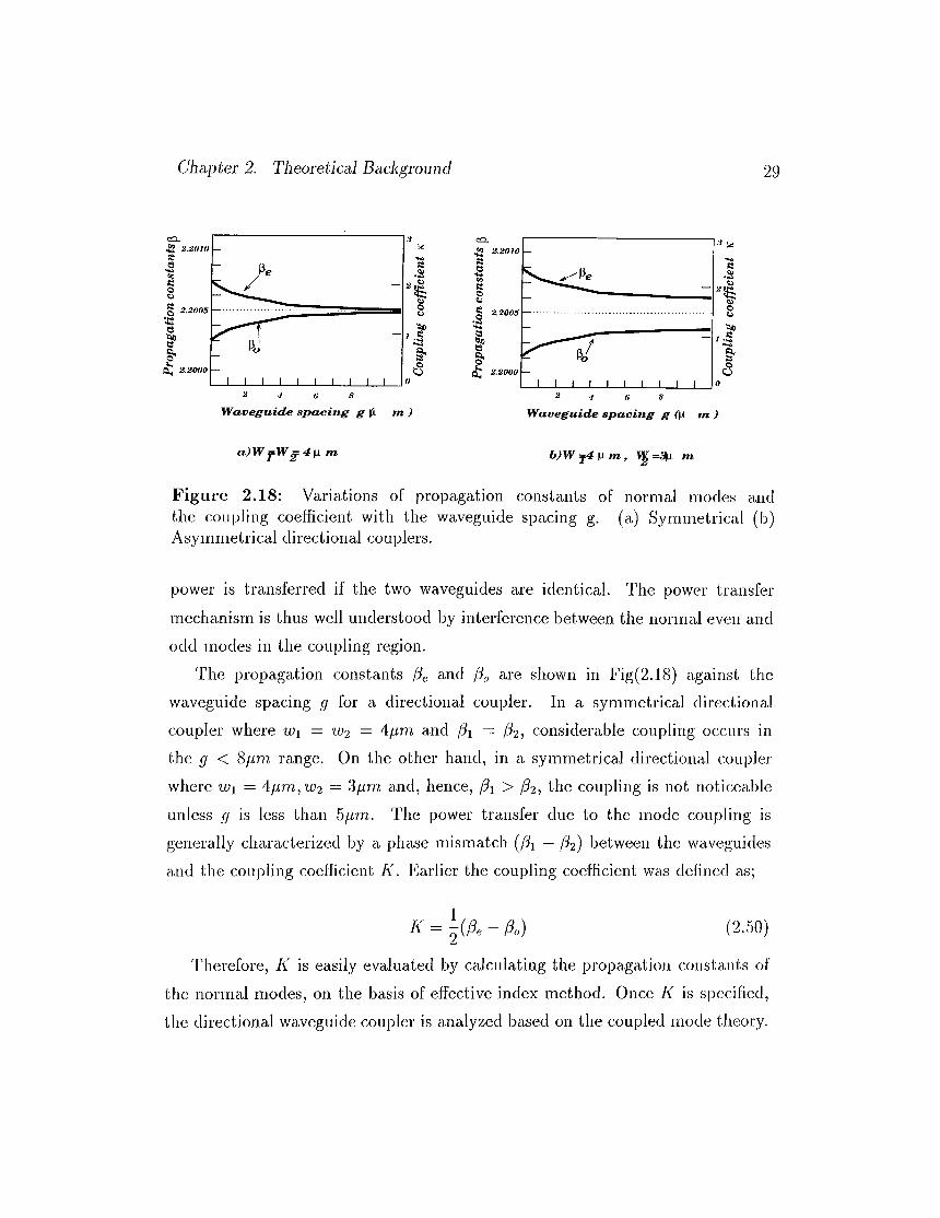
2.16 Power transfer between the coupled waveguides................................ 262.17 Operating principle of waveguide directional coupler....................... 282.18 Varicitions of propagation constants of normal modes and the
coupling coefficient with the waveguide spacing g. (a) Symmetriccil(b) Asymmetrical directional couplers................................................ 29
3.1 MBE grown double heterostructure for Directional coupler . . . . 33
VI

3.2 An etched rib on the double heterostructu re .................................. 343.3 Expected rib geometry after wet e t c h ............................................... 353.4 Cross sectional view of the coupler in the coupling reg io n .............. 353.5 The structure which we solve for the regions I, III, cind V. 363.6 The structure which we solve for the regions II, and IV.................. 363.7 The coupler problem reduced to an effective one dimensional
geometry.................................................................................................. 373.8 The guided mode changes its polarization in the effective geometry. 373.9 Five layer slab geometry........................................................................ 383.10 Three layer slcib geometry..................................................................... 42•3.11 Coupler geometry.................................................................................. 443.12 Effective geometry of the coupler......................................................... 46
3.13 TE, TM coupling lengths as function of coupler gap for ridge widthw of 3^im, aluminium cone. x==0.3, and the lateral clad, t of 0.3p'm. 48
3.14 TE, TM Coupling Lengths as function of coupler gap for ridge width w of 3/«??r, aluminium cone. x=0.3, and the lateral clad, tof 0.2/j,7ti.................................................................................................. 48
3.15 TE, TM coupling lengths as function of coupler ga]) for ridge widthw of 2.5/J.rn, aluminium cone. x=0.25, and the lateral clad, t of 0.2/xm....................................................................................................... 49
3.16 TE, TM coupling lengths as function of coupler gap for ridge widthw of 3.5/^m, aluminium cone. x=0.25, and the lateral clad, t of 0.2¡jLm....................................................................................................... 49
3.17 TE, TM coupling lengths as function of coupler gap for ridge width
w of 3/i?7r, aluminium cone. x=0.25, and the lateral clad, t of Q.2/j,rn. 503.18 TE, TM coupling lengths as function of coupler gap for ridge width
w of ciluminium cone. x=0.25, and the lateral clad, t of 0.2p?/i. 503.19 TE, TM coupling lengths as function of lateral cladding thick, t
for ridge width w of 3/um, aluminium cone. x=0.3, and the couplergap g of 4.5/7777........................................................................................ 51
vn
3.20 TE, TM coupling lengths as function of ridge width for couplergap g of 3//??r, aluminium cone. x=0.25, and the lateral clad, t of 0 .2 f j, rn ....................................................................................................... 51
3.21 TE, TM coupling lengths as function of aluminium cone, x for ridge width w of 3/^m, coupler gap g of 3/um, and the lateral chid.t of 0.2/1771................................................................................................ 52
3.22 Single-Multi mode regions depending on the Lateral Claddingthickness t vs. aluminium concentration x......................................... 52
3.23 Coupling of the TE and TM modes; one crosses over while theother is coupling back for our optimum coupler design.................... 53
3.24 Geometry of the etched ridge............................................................... 543.25 Single-multi mode regions depending on the guide ridge with tu
and the lateral cladding thickness t ..................................................... 55
3.26 Cross section of the devive at the coupling region.............................. 563.27 Top view of the coupler with bended sections..................................... 563.28 3-D vector BPM simulation for the TE guided mode of the coupler
geometry shown in Figure (3.27) with straight coupling section of 3300 /rnr................................................................................................... 57
3.29 3-D vector BPM simulation for the TE guided mode of the couplergeometry shown in Figure (3.27) with straight coupling section of 3500 /1777................................................................................................... 58
3.30 3-D vector BPM simulation for the TE guided mode of the couplergeometry shown in Figure (3.27) with straight coupling section of 3900 iim ................................................................................................... 58
3.31 3-D vector BPM simulation for the TE guided mode of the couplergeometry shown in Figure (3.27) with straight coupling section of 3700 /im................................................................................................... 59
3.32 3-D vector BPM simulation for the TM guided mode of the couplergeometry shown in Figure (3.27) with straight coupling section of
3900 /7777. 59
vm
3.33 An example of the cascaded field profile movie obtained from theoutputs of the 3-D vector BPM simulations for the TE guided mode of the straight coupler with a gap of 4.5yu??z and a propagation distance of 4000 ¡.tm............................................................................... 60
3.34 The applied field and the guided modes; the field of TM mode is nearly along the applied field, therefore no index change for theTM guided mode.................................................................................... 64
3.35 Top view of the device with counter electrodes. 65•3.36 Toi5 view of the device with push-pull electrodes. 654.1 SEM iDicture of the GaAs/AlGaAs double heterostructure.............. 674.2 PL spectrum of GaAS layers in our wafer. 694.3 PL spectrum of AlGaAS layers in our wafer...................................... 704.4 Raman spectrum of GaAs and AlGaAs layers................................... 714.5 Etch profiles for different crystall orientations................................... 764.6 Sccinning Electron Microscope (SEM) picture of the etched ridge
with the Wright guide crystall orientation giving the desired etch shape and the lithograiDhic photoresist on it ...................................... 76
4.7 SEM picture of the etched guides, side wall smoothness isimportant to prevent losses................................................................... 78
4.8 SEM picture of the guides with metal electrodes deposited on topof ridges................................................................................................... 82
4.9 Optic microscope iDicture of the connection with the electrodes ontop of the guides cind the pads............................................................. 82
4.10 Optic Microscope picture of the Push-pull type electrodes.............. 824.11 Optic microscope picture of the alignment marks from a processed
sample...................................................................................................... 834.12 Mask layout; three layer mask with the layer 1 the guide etch mask,
hiyer 2 the electrode metallization, and layer 3 the pad metal mask.
The devices are in a 11,920 x 9,750 ¡JLin mask area......................... 844.13 Marks for initial rough a lig n m en t..................................................... 854.14 Marks for fine cilignment....................................................................... 85
IX
4.15 Descriptions of the devices on the mask............................................ 864.16 Descriptions of the devices on the mask............................................ 875.1 Representative picture of the coupling ratio measurements............. 905.2 The iDcirameters of the fabricated passive devices.............................. 91
5.3 Coupling fraction, Push Pull (PP.) elect., g=4.5/i?7?., ιυ — 3μηι. . . 915.4 Coupling fraction. Counter Elect. (C.E.), g=4.5^m, w = 3μΐη. . . 925.5 Coupling fraction of modes for g=4.75/im cind w = 3μητ................. 925.6 Coupling fraction of modes for g■=A.^^μm and w = Ζμπι................. 935.7 Coupling fraction of modes for g=4.25/«?ri and w = Ζμτη................. 935.8 Coupling fraction of modes for g=4.25/«m and w - '3μηι................. 945.9 The parameters of the fabricated active devices................................ 955.10 Parameters of the fabricated active device......................................... 955.11 Coupling fraction of modes for g=4:.bμm and w = $μπι................... 965.12 Coupling fraction of modes for g—4:.25μm and w — 3μητ................. 965.13 Coupling fraction of modes for g=4.75μm and w = 3μτη................. 975.14 Coupling fraction of modes lor g—4:.75μm and w — 3μτη................. 975.15 Least square fit to the Equation (2.47) of the TE data for g=4.5 i?77,
without bias............................................................................................ 985.16 Least square fit to the Equation (2.47) of the TE data for g='\ J)μm
under a bias V=10................................................................................. 985.17 Least square fit to the Equation (2.47) of the TM data for g=4.5^?77,
without bias............................................................................................ 995.18 Least square fit to the Equation (2.47) of the TE data for
g=4.25^?77 under a bias V=30.............................................................. 995.19 Least square fit to the Equation (2.47) of the TE data for g=4.5/i?77,
under a bias V=10................................................................................. 995.20 Calculated vcilues of K for TM and biased-unbiased TE as a
function of gap........................................................................................... 101
X
Chapter 1
Introduction
Integrcited optoelectronic devices made of semiconductors, particukirly semiconductor compounds, have cittracted considerable interest in recent years. Such components may form the basis for integrated optoelectronic circuits in which light sources and detectors, as well as optical waveguide devices and electronic circuitry, are monolithically integrated on the same substrate. Through integration, a more compact, stable, and functional optical system can be expected. Many research groups all over the world are studying to realize this goal.
Optical functional devices that manipulates the light while in transmission are components that have a key position in the present cind future technological devices. External optical switches and modulators of multigigahertz
bandwidth and high optical power handling capacity Imve a multitude of applications in the present and future fiber optic systems, not only
for telecommunications but for airbone and satellite-based phased cirray radcir and instrumentation, and for optical signal processing applications. Reseiirch on bulk optical switches and modulators began shortly after the invention of the laser several decades ago. The goal of efficient high-speed devices stimulated
researchers throughout the world to seek better electro-optic nicitericils and efficient device geometries. With the rapid reduction of loss in glass fibers in the late sixties, research on optical switches and modulators gained new stimulus
1
Chapter 1. Introduction
cind new directions. Waveguide devices were investigated j^rimarily because of their compatibility with fibers and the ultimate goal of integration.
Directional couplers are building blocks for many guided wave devices in integrated optics and optoelectronics.They have been used as switches, modulators, wavelength filters, wavelength multiplexer and demultiplexers, and power d i v i d e r s . A s optical switches made of semiconductor waveguides, they are important for future switching networks. The interest in guided-wave optical switches is growing as the signal bit rate in transmission over optical fibers becomes higher, because of their data path transparency.® They are also very important devices for the external modulation of lasers at high data ixite. They cire basically the key devices in an integrated circuit being the intermediate position of manipulating and controlling lightwaves and signals in between sources cind recievers.
A directional coupler consists of a pair of closely spaced, parallel waveguides. The interaction of the evanescent fields of the guided modes in the individual waveguides causes power exchange between the coupled waveguides. The power trcinsfer can be controlled by adjusting the synchronization and the coupling coefficient between the guides. An attractive feature of this coupling effect is its sensitivity to small changes in the values of the structure parameters, relVcictive indices, interguide spacing, guide width, allowing easy control of the energy exchange between the coupled waveguides, by external fiictors such as electric, magnetic, and acoustic fields.®
Up to date several types of directional couplers have been realized with different working principles and on different material systems. Waveguides are the
basic tools for couplers, so the material used is important for the purpose. Simply it is the material refractive index difference that is utilized to obtain a waveguide to guide the optical modes. These guides are formed by directly growing different index materials on top of each other in the desired way as well as creciting this index difference through an applied field, as in the case of field induced guides (FfG’s). Directional couplers using this type of guides were realized.^ Carrier injection type switches,^ gain guide type switches, electrooptic, acousto-optic'
Chapter 1. Introduction
directional couplers,'* vertical directional couplers, FIG type directioiuil couplers, nonlinear directional couplers'* are of a few examples of directional couplers constructed so far.
The material system on which the directional couplers are fabricated is another important parameter. Lithium Kiohate(LiNbOs), InGaAsP/ InP, GaAs/AlGaAs are examples of material types used for waveguides in couplers. Considerable efforts have been made to study LiNhOs optical switches** for such applications as space-division, time-division, and wavelength division photonic switching.® Couplers for lightwave systems made of LiNbOz hcive achieved very high distance times data rate products.® Although LiNbOs ojDtical switches and couplers have attractive features, like low propagation loss and low coupling loss to single-mode optical fibers, they also have drawbacks, such as large device size, cuid the inability to be integrated with other active optical devices, which prevent the LiNbOz switches from being realized into large scale integration.® Therefore, there has been considerable interest in opticcil switches made of III- V semiconductor compounds for those applications, because of their large scale integration capability and their ability to be integrated with other semiconductor devices in order to realize the ultimate goal of Photonic Integrated Circuits
(PIC’s).This thesis describes work on the polarization splitting GaAs/AlGaAs
directional couplers. For successful! utilization of optical intensity modulation devices in commercial systems, such as optical switches and moduhitors which hcive many important apj^lications in broadband communications, optical control of microwave and milimeter wave signals and instrumentation for high speed
real time signal processing, several requirements should be met. These are wide electrical bandwidth, low microwave power consumption, hirge optical extinction ratio and dynamic range, low ojDtical insertion loss and polarization independence.Polarization independence is a crucial point for the present cind
future applications of guided wave devices.It has long been recognized that IITV semiconductors offer significcint
advantages over other materials such as LiNbO^}^ These include the potential for
Chapter 1. Introduction
monolithic integration with other optolectronic and electronic devices to enhance the functionality of transmitter and reciever circuits using additional guided-wave signal processing, suitability for high-speed low-drive voltage modulators and switches“ with further advances expected from multiple quantum well (MQW)
technologies,“ and the availibility of sophisticated, controllable fabrication processes (e.g. epitaxial growth, selective etching) and simple methods for end facet preparation (scibe-and-cleave versus cut and polish). The advantages offered by III-V materials, however, have historically been offset by the high insertion loss(> 3 dB) of semiconductor waveguide devices cind the large size (> 1 cm) of conventional integrated optical circuits. Device insertion loss directly reduces the maximum transmission length of communication systems, cind is therefore highly undesirable. A second issue is large device size and incompatibility with the relatively high cost of III-V semiconductor materials.“ Nonetheless, significant progress has occured in the areas of loss and chip size during the past several years. The results of the studies showed that insertion loss cilone, including the problem of fiber coupling, is no longer a serious barrier to the use of III-V semiconductor integrated optics. As a result of improvement in epitaxial growth and waveguide channel fabrication techniques, straight guide propagation loss has also been reduced to levels comparable to that in LiNbO^,^'^ and to the point where overall insertion loss is usually dominated by other factors. Therefore, among all types of optical switches, a GaAs/AlGaAs electrooptic directional coupler is attractive as a cross point element for an integrated switch, because of its low absorbtion loss at long wavelength r eg i on , f a s t switching speed, low electric power consumption, and wavelength independent operation capability with the advantages of more advanced microfabrication technologies.®
In our design of the polarization splitting directional couplers, optical waveguiding is realized using rib waveguides etched into a GaAs/AlGaAs heterostructure, which is unintentionally doped and MBE grown on a [100] oriented semi insulating substrate. Due to depletion originating at the surface and semi insulating substrate interface, it is almost self depleting. Confinement of the guided mode in the guide is ¡performed by utilizing the effective index differences.“
Chapter 1. Introduction
To handle the polarization and polarization sensitivity, we incorporate tunability with the help of rnetal electrodes from Schottky contacts with GaAs/AlGaAs heterostructure, rather than using entirely passive couplers. The bulk electrooptic effect is used to achieve index change with the applied field. The coupler we have designed is basically formed by symmetric waveguides that have bends at both the inputs and the outputs to separate the guides from each other which are coupled in a so called ’’coupling region”. These bends critically effect the device size. To seperate the guides that are coupled with a 7.5 prn centre to centre distance to a point of 30 pm seperation, a distance of 3000 pm is required, because of optimum curvature needed to have minimum loss. Effective index method calculations were used to cinalyse the rib geometry waveguides, to obtciin the guided modes and propcigation constants. The coupling lengths of the guided TE and TM modes were then calculated. The device is designed so that only one mode will be able to propagate through the guides, since the coupler is a single mode operating device. The design of the polarization sensitive couplers using these optical waveguides were carried out using the 3-D Vector beam propagation method (BPM) codes that were developed previously.N um erous simulations of the theoretical design were performed to test the structures and to reach the optimum design parameters for low loss and comjDact geometry. Our basic goal was to obtain a geometry that have passively coupling lengths (Lc) for TE and TM modes of which the L dT M ) is twice as much as the Lc{TE). This results in splitting of TE and TM polarizations at the outj^ut jDorts. The electrooptic efhect is used to change and tune the coupling lengths by an applied DC bias to the Schottky electrodes over the guides in the coupling region. The applied electric
field induces a change in the refractive indices under the rib geometries which effect the coupling lengths of the TE and TM modes differently. This allows the possibility to route TE polarization to the desired output port. So this enables us to achieve easy contx’ol of the coupling of the modes with the applied field, resulting a coupler that can be placed a through state for TE or for TM polarized guided modes.
In the following chapters, we show that polarization insensitivity can be
Chapter 1. Introduction
realized in the GaAs/AlGaAs double heterostructure material system, with low loss and compact geometry ready to be integrated to other polarization related devices or optical circuits rnonolithically or hybrid type. In Chapter 2, we summarize the basic principles of the theory of waveguides with special emphasis on the planar and rib waveguides, calculations of the guided modes and their properties, optical losses and dispersion in waveguides, brief introduction to the coiq^led mode theory cuid the Bea.rn Propagation méthodes, the effective index method, and an introduction to the basic theory of operation for directional couplers.
I l l chapter 3, we present our work on the design of the Polarization Sensitive Directional Couplers. The geometries used and the effective index method calculations used to obtain a single mode, low loss compact geometry , calculcitions of the coupling lengths for the TE & TM polarizations and, results of the Beam propagation Method (BPM) simulations are presented. Finally, a brief description of the mask design and the mask features are given.
Chapter 4 contains a detailed description of the fabrication of the devices, with standard processing equipment and techniques, optimization of process pai’cimeters especially for obtaining guides of milimeters long and a few microns of thickness. We begin with characterization of the starting wafer grown for this purpose with SEM, and optical spectroscopy and explain the processes to
fabricate the device.ChaiDter 5 describes the characterization and testing of the Polarization
Sensitive Directional Couplers, with a brief description of the test setup, and
the results.
Chapter 2
Theoretical Background
The fundernantal idea behind the integrated optics is to handle light with waveguides, cind not by free space optics. Nearly in all opticcil devices, opticcd held is guided by dielectric waveguide structures, i.e, by properly shaped dielectric prohles. Although, rnetal clad structures represent an alternative way for Wcive- guiding that is popular for microwaves, they are rarely used in integrcited optics ci.s the metals are too lossy in the optical wavelength region. The main results of the waveguide theory are the number of guided modes for a given dielectric profile, the effective index and the optical field for each mode. A siricdl number of devices call for the analysis of the radiation field and, in particular for leaky
modes, i.e, for resonances in the radiation field. These result, in turn, form the basis of device modeling, e.g, of the coupled mode theories describing directional couplers.
Waveguide analysis requires the solutions of partial differential equations, i.e
a recisonable cimount of computer power. As a consequence, a lot of work in the pioneering days of integrated optics was focused on approximations such as the effective index method (EIM) or Marcatili’s m e t h o d . W i t h the increasing power of computers, increiisingiy numerical solutions such as finite element (FE),^^ finite difference (FD)^^ and method of lines (MoL)^^ cilgorithrns cire used to analyze waveguide structures. Nevertheless, approximate methods in general and the effective index method in particular represent the work horses for design and
modeling of optical waveguide structures.
Waveguides used in integrated optics today are all defined by lithographical techniques, usually by contact of projection lithography, sometimes by direct electron beam writing. The fabrication of the rib, buried rib, strip and strip loaded waveguides involves usually an etching process such cis wet chemical etching, reactive ion etching (RIE), or reactive ion beam etching (RIBE). The choice of process and the required aspect ratio i.e. Etching depth / structure size determines the shape of the waveguide, its roughness, and importantly the fabrication tolerances, especially the waveguide width. For the III-V semiconductor material systems, the layers of different materials for these waveguides are grown by epitaxy, usually by metal organic vapor phase epitaxy (MOVPE), or metal organic molecular beam epitaxy (MOMBE), or sometimes by liquid phase epitaxy (LPE). In contrast, for the silica-on-silicon matericil system (SiO-i/Si), the layers are fabricated by deposition - various types of chemical vapor deposition (CVD), or flame hydrolysis, or by thermal o x i d a t i o n . T h e choice of the fabrication process defines the ranges of available layer thickness and
material compositions. In addition, it determines the roughness of the interfaces cuid the fabrication tolerances of the material composition and the layer thickness.
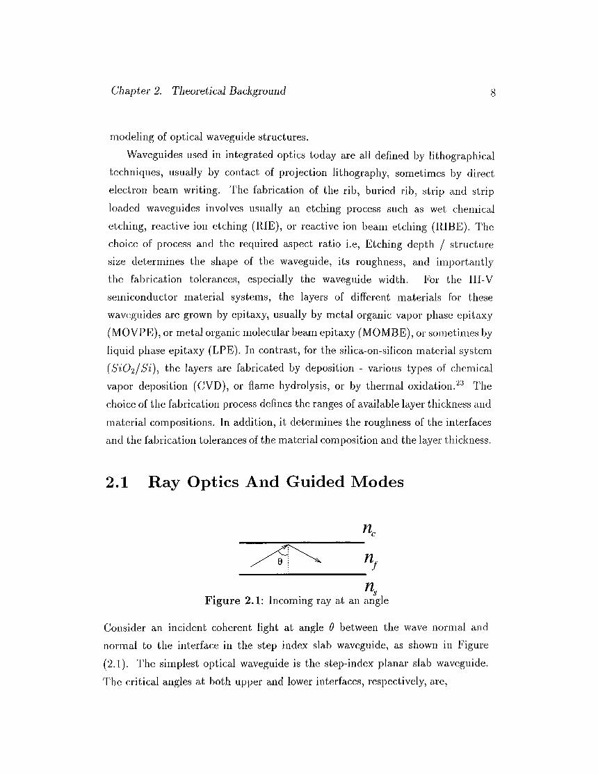
2.1 R ay O ptics And Guided M odes
Chapter 2. Theoretical Background 8
n.
nf
Figure 2.1: Incoming ray at an angle
Consider an incident coherent light at angle 6 between the wave normal cind normal to the interface in the step index slab waveguide, as shown in Figure
(2.1). The simplest optical waveguide is the step-index planar slab wciveguide. The critical angles at both upper and lower interfaces, respectively, are.
Chcipter 2. Theoretical Background
Oc = shi '(nc/nf) O s - s i n ^ { n s l r i f ) (2.1)
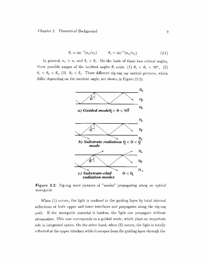
In genei’cil, > rp, and Os > 0 . On the basis of these two criticid angles, three possible ranges of the incident angles Oi exist: (1) Os < 0i < 90°, (2)Oc < O2 < Os (3) 3 < Oc- Three different zig-zag I'ciy optical pictures, which differ depending on the incident angle, are shown in Figure (2.2).
a) G u id e d m odeB < 0 < 96
b) S u b stra te ra d ia tio n 0 < 0 < 0 m o d e
c) S u b stra te -c la d ra d ia tio n m o d es
0 < 0..
Figure 2.2: Zig-zag wave pictures of ’’modes” propagating along an o waveguide
tical
When (1) occurs, the light is confined in the guiding layer by total internal reflections at both upper cind lower interfaces and propagates cdong the zig-zcig path. If the waveguide material is lossless, the light can j^ropagate without attenuation. This case corresponds to a guided mode, which phiys an important role in integrated optics. On the other hand, when (2) occurs, the light is totally reflected at the upper interface while it escapes from the guiding layer through the
Chapter 2. Theoretical Background 10
cover according to Snell’s law, because 0 < 6 . The light is a substrate radicition mode whose cimplitude decreases significantly along the propagation direction. The 0 < $c Ccise also lecids to substrate-clad radiation modes that rcidiates to both the cover and the substrate. As discussed earlier, modes can be classified
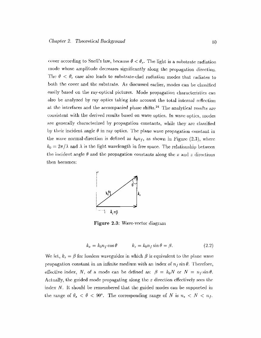
easily based on the ray-optical pictures. Mode propagation characteristics can also be analyzed by ray optics taking into account the total internci.1 reflection at the interlaces and the accompanied phase shifts. '* The cinalytical results cire consistent with the derived results based on wave optics, in wave optics, modes are generally characterized by propagation constants, while they are classified by tlieir incident angle 0 in riiy optics. The plane wa.ve propagation constant in the wave normal-direction is defined as AiqU/, as shown in Figure (2.3), where ko — 27t/A and A is the light wavelength in free space. The relationship between the incident angle 0 and the propagation constants along the x and directions then becomes:
Figure 2.3: Wave-vector diagram
kx = konfcos0 kz = koiif sinO = /3. (2.2)
We let, kz — [3 for lossless waveguides in which ¡3 is equivalent to the plane wave propagation constant in an infinite medium with an index of nj sintl. Therefore, effective index, N, of a mode can be defined as: (3 = koN or N = rifshiO. Actually, the guided mode proj^agating along the 2; direction effectively sees the index N. It should be remembered that the guided modes can be supported in the range of 0,, < 0 < 90°. The corresponding range of N is 77,,, < N < rij.
Chapter 2. Theoretical Background 11
Sirnilcirly, the radiation modes exist in the range of N < iig.
2.2 W ave Equations For a Slab W aveguide
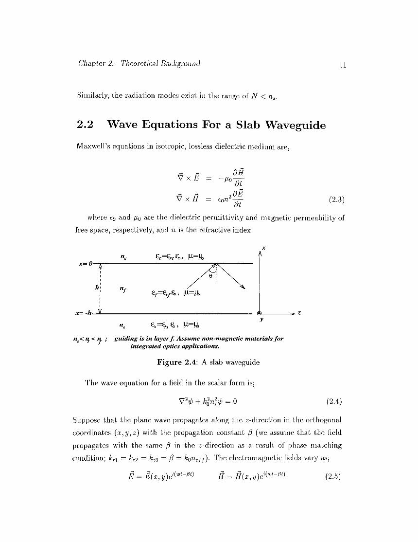
Maxwell’s equations in isotropic, lossless dielectric medium are,
V7 f 'V x £ =
V x / / - e o n ^ ^ (2.3)
where cq and go are the dielectric permittivity and magnetic permeability of free space, respectively, and n is the refractive index.
; guiding is in layer f. Assume non-magnetic materials for integrated optics applications.
Figure 2.4: A slab waveguide
The wave equation for a field in the sccilar form is;
+ klnf-if) = 0 (2.4)
Suppose that the plane Wcive propagates along the ^-direction in the orthogonal coordinates {x,y,z) with the jDropagation constant /3 (we assume that the field propagates with the same ¡3 in the ’r-direction as a result of phase matching condition; kzi = k ,2 = k^ = ¡3 = koUeff). The electromagnetic fields vary as;
= A’(.T,2/)eT H = H{x,y)e (2.5)
Chcipter 2. Theoretical Background 12
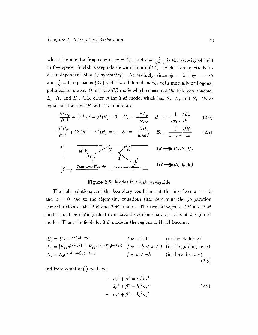
where the angular frequency is, w = and c = is the velocity of lightin free space. In slab waveguide shown in figure (2.4) the electromagnetic fields are independent of y (y symmetry). Accordingly, since ^ = iw, ^ — —i/S and ^ = 0, equations (2.3) yield two different modes with mutually orthogonal polarization states. One is the T E mode which consists of the field components, Ey^ IE and Hz. The other is the T M mode, which has E^, IIy and i?,,. Wave equations for the T E and 'TM modes are;
diE,dx^
dHlydx'^
■ + {kf^nf - I}'‘)E, = 0 II - tr _ 1 (2.6)WjlQ Z - · r\iwfio dx
+ {ko^Ui -- = 0 E - _ i dH, (2.7)ilOtoU' dx
TE
TM.
(Ey’fi
Figure 2.5: Modes in a slab waveguide
The field solutions and the boundary conditions at the interfaces x — —li and a; = 0 lead to the eigenvalue equations that determine the propiigation characteristics of the T E and T M modes. The two orthogonal T E and T M modes must be distinguished to discuss disj^ersion characteristics of the guided modes. Then, the fields for T E mode in the regions I, II, III become;
Ey = EcC for a; > 0 (in the cladding)Ey — for — h < x < 0 (in the guiding layer)
_ £J [ois{x+li)] {-ikzz) for X < —h
and from equation(.) we have;
k J + /3 = k o W
(in the substrate)(2.8)
(2.9)
Chapter 2. Theoretical Background 13
Applying the boundary conditions at the interfaces at a; = 0 and x = and the fact that tangential components of the fields E and H are continuous;
i?,X0+) = AV(O-), Ey{h-) = Ey{h^) and /A ( /r ) = /f,(h+)
(2 .10)for x > 0
(2.11)
hL = IXUB-Q■ ( /7 - for h < X <0
f o r x < - hand eliminating the unknowns from the equations, we obtain an eigenvalue equation;
cy -4- rv„(2.12)
I 1 “h CistanA:^/i 7—7---------- -t ( i - 1 ? )
The same ¿inalysis ¿ipplies to the T M mode and an eigenvalue equation for T M is obtained;
T) 2 CVcia n k j i = — ----VicJ — (2.13)
■ ns2 kx /V Uc kx /If the structure is symmetric then ric = Ug and ac — cxs = a. There are two choices for the description of the field in the guiding layer, depending on whether a symmetric (cosine) or antisymmetric (sine) mode is excited. The fact that the modes can be uniquely characterized in terms of even or odd groups is a natural consequence of the even symmetry of the index structure. The sign of the field in the lower substrate is positive for the even modes, and negative for the odd modes. The characteristic eigenvalue equation for the T E modes in a symmetric waveguide is:
,kJi^ \ f - for even(cos) modest a n ( - ^ ) = < ^ \ ^
2 for odd (sin) modes
The characteristic equation for the T M modes is;
,k^h. I { ^ ) f- for even(cos) modesmodes
If we rearrange the eigenVcilue equation for the symmetric T E mode;ahT
kg h kg hi—— tan ——
(2.14)
(2.15)
(2.16)
Clmpter 2. Theoretical Background 14
and using the relations for the propagation constants;
k j + I3 = k o W
—Oix -l· — ko iic^
to obtain;.k^H, ocxh k(j h . 2 2\
(2.17)
(2.18)
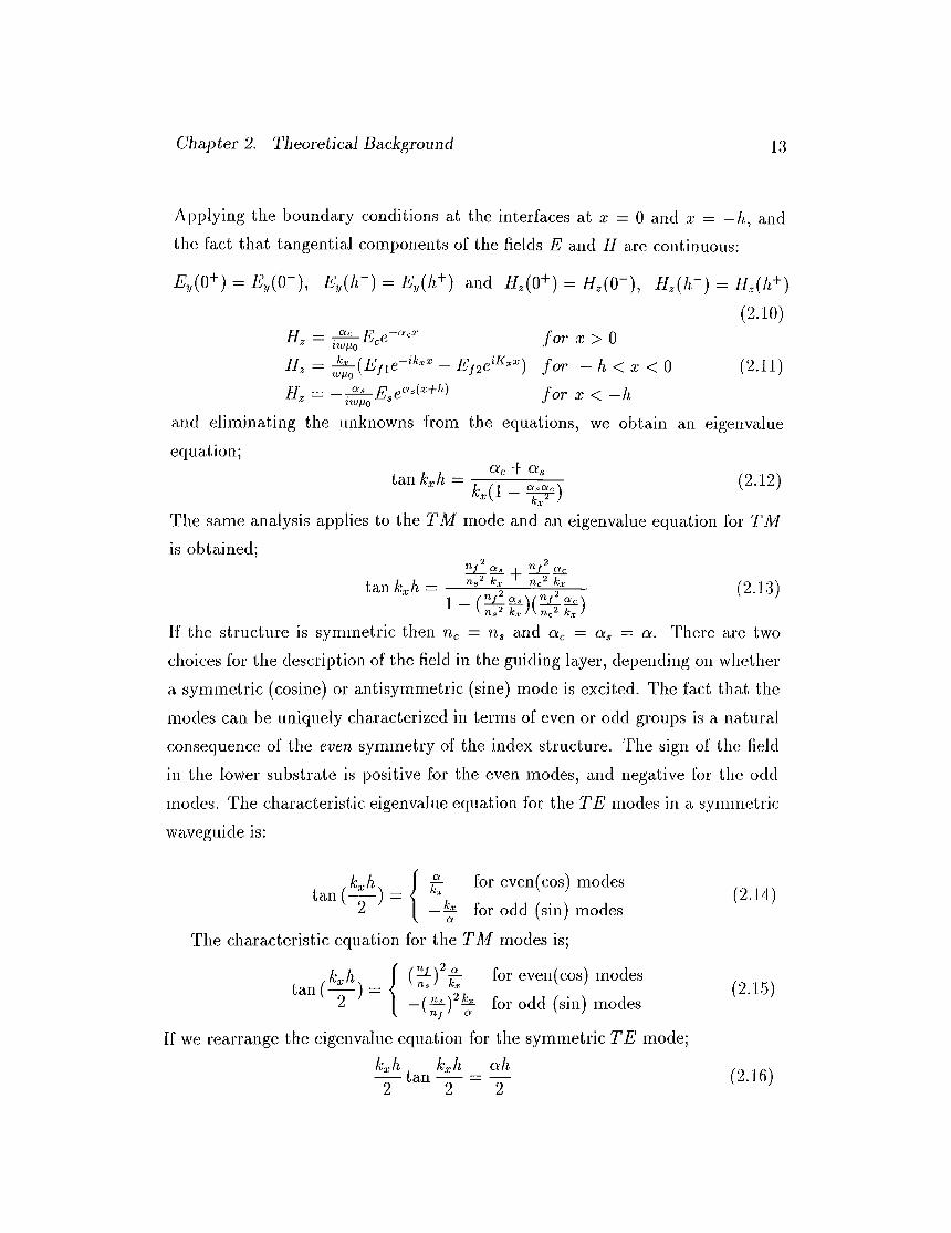
and defining x = ( ^ ) and y = ( ^ ) , we obtain the following curves as solutions lor the eigenvalue equations. Number of guided modes in the structure will depi'iid on the iDarameter where ~
Figure 2.6: Parametric solutions of the eigenvalue equation
The guided modes are in the range kgUg < /d — koUeff < kouj. The following definitions can be used to obtain a normalized eigenvalue equation;
■n 2 ... 2Ux — Kc.nj^ - U s “
where the asymmetry parameter is in the range;
(Asymmetry Pariimeter) (2.19)
a —0 lor symmetric slab geometry0 < a < oo for asymmetric slab geometry
(2.20)
When the waveguide parameters are given, the eigenvalue equation can be
solved numerically to evaluate the dispersion characteristics of the guided modes. Such a numerical evaluation is applicable to any step-index 2 — D waveguide
Chapter 2. Theoretical Background 15
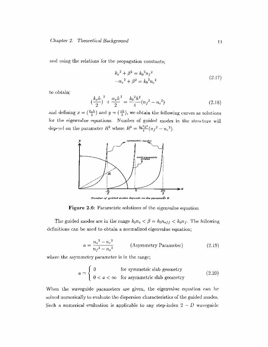
l î y ( x )
Figure 2.7: Optical electric field clistrubutions of TE guided modes.
by introducing the following normalizations: Normalized frequency (normalized thickness) V and the normalized guide index b are defined cis;
V — koh^Jn/^ — Us' (2.21)
n - n ^b = ^ (normalized index, 0 < 6 < 1)
— n /(2.22)
Using the above definitions the eigenvalue equation(2.12) Ccin be written cis;
V V i — b = tan -----^+tan ^y ----^(normalized eigenvalue equation tor TE)
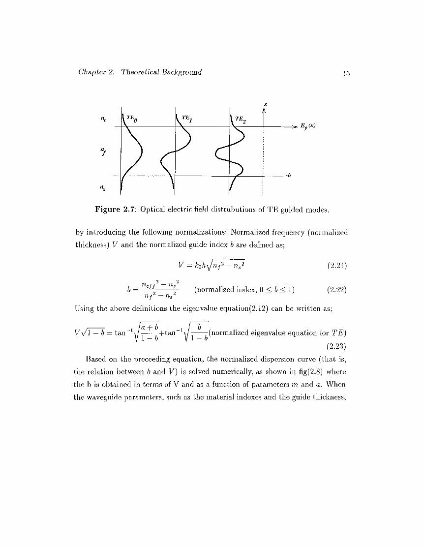
(2.23)Based on the preceeding equation, the normalized dispersion curve (that is,
the relation between b and U) is solved numerically, as shown in fig(2.8) where the b is obtained in terms of V and as a function of parameters m and a. When the waveguide parameters, such as the material indexes and the guide thickness.
Chapter 2. 'Theoretical Background 16
Figure 2.8: Normalized Dispersion Curves.
Chapter 2. Theoretical Background 17
are given, the effective index of the guided mode is obtained graphically. The waveguide parameters ¿ire usually determined on the basis of cut off of the guided modes. When the incident angle 0 becomes the critical angle Og, the light is no longer confined in the guiding layer, and it begins to leak in to the substrate at the interface x = —h. This situation is called cut off of the guided modes, in which the effective index n^ff = ns(b = 0). From the normalized equation, the Vcdue of V at the cut off is given by;
V = tan /cı + rmr = f/f, + rmr (2.24)
Vo is the cut off value for the fundemantal mode. If the normalized frequency V of the waveguide ranges over Vm < V < Idn+i, the TE q, TEi - ■ ■ and the Ti?,« modes are supported; the number of the guided modes is + 1. For symmetrical waveguides [ug = iic), Vo = 0. This implies that the fundemantal mode is not cut off in a symmetrical waveguide.
For the T M modes, the analysis is similar to the preceeding. Since Hy cind Eg: are continuous at the interfaces, however, a square of the index ratio is additionally included in the eigenvalue equation;
v V T (2.25)c ]j 1 — b ' c — a \ 1 — b
The above is the normalized eigenvalue equation for T M modes where c is defined as c = —
2.3 Effective Index M ethod
Mode structure analysis of semiconducting waveguides are difficult and require detailed calculations. In this section, a method known as the effective index method is introduced briefly. However, there are cipproximate methods that usually give quite accurate results for design purposes. This method gives universal dispersion curves of the normalized parameters (6, F, a) for slab
Wciveguides.
Chapter 2. Theoretical Background 18
Figure 2.9; 3-D waveguide with a step-index profile
Figure (2.9) shows an analytical model where a step-index rectangular Wcivcgiiide is surrounded by different dielectric materials. Under the well-guided mode condition, most of the optical power is confined in region I, while a smcill amount of power travels into Regions II, III, IV, and V, where the electromagnetic fields decay exponentially. Even less ¡Dower should penetrate the lour slmded areas. Only a very small error, therefore, should be included in calculating the fields of the guided mode in Region I provided the field matching at the four corners of the shaded areas is not taken into account.
The effective index method converts a two-dimensional problem into two, one dimensional problems. Consider the buried step-index rectangular waveguide shown in Figure (2.10a).
X
JS)
n„
n.
w.■ ^ y
(a)
n„
n„(b)
Figure 2.10:
ne f f
(c)
n .
To use the effective index method, we first stretch the waveguide out along its thin cixis (in this case cdong the y-axis) forming a i lancir shib waveguide. Figure (1.9b). The thin one-dimensional slab waveguide can now be cinalyzed in terms
Chapter 2. Theoretical Background 19
of T E and T M modes to find the allowed value of fd for the wavelength <ind mode of interest. Once /3 is found, the effective index of the slab is determined through the expression nefj = where A:o is the vacuum wave vector of light being guided. After this effective index is determined, we return to the original structure and now stretch it along the thick axis, in this case along the x cixis, forming a slab waveguide in the x-direction. Figure (1.9c). The modes for this Wciveguide can now be found in a similar fashion, only instead of using the original value of the index for the guiding him, the effective index found in the first step must be used. The value of ¡3 to be found from this last step is the true value tor the mode.
As with the wave analysis, one must be careful to use the proper characteristic equations tor each waveguide. For examj^le, if in the figure above, the electric field is polarized in the .x-direction, then for the thin waveguide the field will act cis a T M mode, and the cippropriate characteristic equation must be used. When the thick slab is analyzed, this same held will look like a T E mode, and so the characteristic T E equations should be used to find ¡3. When the index difference between the guiding and the cladding hiyers is large, using the proper characteristic equations is critical for getting a reasonable answer.
The slab waveguide is a two dimensional structure, providing no confinement of the wave in the ^-direction in Figure (2.4). A slab like structure known as
the rib xoaveguide is often used in optical integrated circuits to conduct light from point to point on a substrate. The rib waveguide geometry is shown schematically
in Figure (2.11).
Figure 2.11: Geometry of a rib waveguide structure.
Chapter 2. Theoretical Background 20
This geometry can be analyzed using the effective index method. Considered separately, regions I, II, III are each a slab waveguide. These regions each have a set of effective indices that can be found from the eigenvcilue equations derived earlier. The effective index approximation^^ provides an accurate approximate solution for the effective index and propagation constant for the entire rib waveguide structure under the following conditions;
• The aspect ratio, ^ (in the figure) must be small,
• The effective indices for regions I, II, and III must be very close to each other.
These two conditions seem stringent but are very nearly met for a wide variety of waveguide structures used in integrated optical circuits.
2.4 Single-M ode 3 — D W aveguides
In multi-mode waveguides supporting more than two guided modes, mode interference and undesired mode conversion due to small disturbances reduce waveguide device performance significantly. To avoid this, most waveguide devices consist of single-mode 3 — D waveguides supporting only the fundernantcil mode. In slab waveguides that we are interested, possible range of the normalized frequency is determined by V — so that the fundemantal modewith the mode number m — 0 is guided while the first order mode with rn = I is
cut off. Using equation (2.24), the range of V,
tan -y/a -f 7T > U > tan ^^/a (2.26)
to meet the single mode propagation requirement can be found easily. The measure of assymrnetry a is zero for symmetrical waveguides, then this gives us the relation or the range for V to have a single mode in symmetrical guides
as;7T > U > 0 (2.27)
Chapter 2. Theoretical Background 21
2.5 Coupled M ode Theory And Coupled
W aveguides
In many optical integrated circuits, guided modes propagate with coupling. Coupling of optical power from one guide to an other one can be analyzed by coupled mode theory. Various guided modes exist in a lossless Wciveguide which is uniform along the propagation direction. These are normal modes (eigenfuctions in boundary value problems) defined by the waveguide structure cind its boundary conditions. An orthogonal relationship holds among the modes. Thus, each mode propagates without mutual coupling and carries power independently.
There are two methods for analyzing optical wave propagation in perturbed (coupling is a perturbation effect) waveguide systems;
1. Compute the normal modes of the waveguide using Maxwell’s equations.
2. Express the perturbed wave behavior by summation of normcil modes in the unperturbed waveguide system.
Method 1 should give a good solution, but the problems can not generally be solved easily. On the contrary, method 2 gives only approximate solutions but is straightforward and simple. This method also allows for a qualitative understanding of essential phenomena, and approximate solution is surprisingly good. Thus, coupled mode theory is a method that can be used to describe the wave behavior in a ¡Derturbed waveguide system by means of the known normal modes of the unperturbed system. Applications of this theory are very broad.
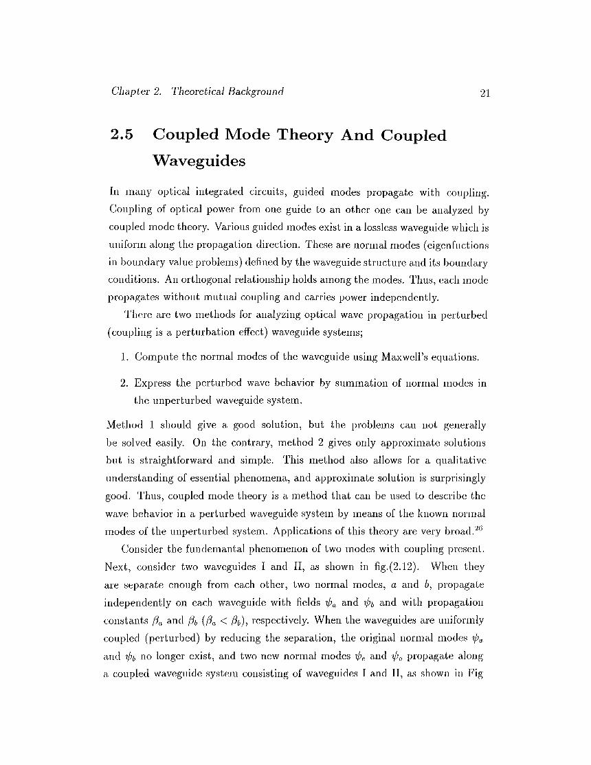
Consider the fundemantal phenomenon of two modes with coupling present. Next, consider two waveguides I and II, as shown in fig.(2.12). When they are separate enough from each other, two normal modes, a and 6, propagate independently on each waveguide with fields ipa and and with propagation constants and ¡3 {fia < /3b), respectively. When the waveguides are uniformly coupled (perturbed) by reducing the sei^aration, the original normal modes ?/>„
and ipb no longer exist, and two new normal modes and i/)o propagate along a coupled waveguide system consisting of waveguides I and II, as shown in Fig
Chcipter 2. Theoretical Background 2 2
u n c o u p le d w a v e g u id e s in a c o u p le d w a v e g u id e sy s te m
Figure 2.12; Norrricxl modes in waveguides in the absence and i^resence of coupling.
(2.12b). ( ?/>e and V'o correspond to a symmetric mode and an cisymmetric mode, respectively.) Propagation constants of these two modes are /3 (larger than
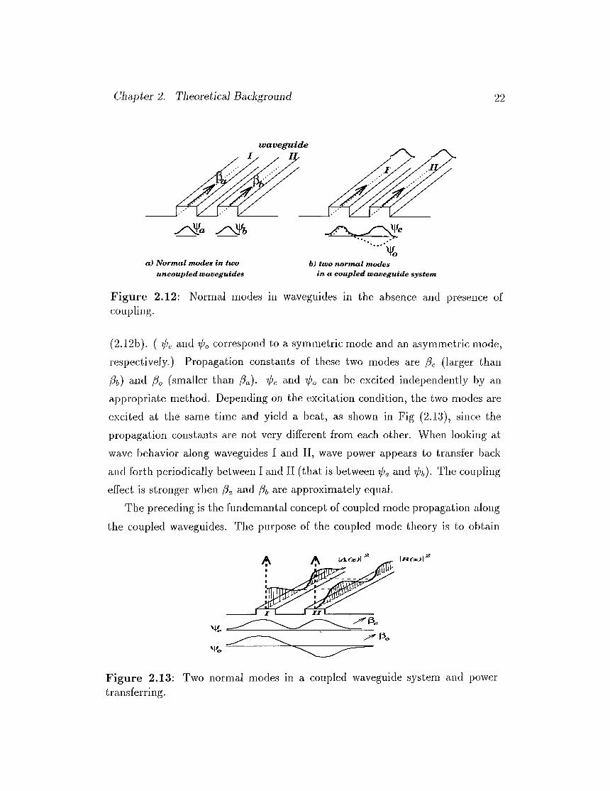
f3b) and f)o (smaller than (ia)· ''/’e and ij o can be excited independently by an appropriate method. Depending on the excitation condition, the two modes cire excited at the same time cind yield a beat, as shown in Fig (2.1-3), since the propagation constants are not very different from each other. When looking at wave behavior along waveguides I and II, wave power appears to transfer back and forth periodically between I and II (that is between ?/>„ and ?/>(,). The coupling effect is stronger when ¡3a and j3b are approximately equal.
The preceding is the fundemantal concept of coupled mode iDi'opagation cilong the coupled waveguides. The purpose of the coupled mode theory is to obtain
Figure 2.13: Two normal modes in a coupled wa.veguide system and power trcvnsferring.
Chapter 2. Theoretical Background 23
?/>e, i/j„, beat period, and other quantities using V>o. and ¡, from coupling features. Opticcxl waves ?/)„ and propagating along the coupled waveguides I and II are expressed as;
y, z, t) = A(z)e (2.28)
y, z, t) = B(z)e~'^'’"fb{x, (2.29)
where fa. and /¡, are field distrubution functions that are normalized by power How over a cross section. If coupling between I and II is reduced to zero, and 'ihh are reduced to two independent original modes, and A(z) and B(z) are reduced to constants. In this case, coupling is present, and therefore, A(z) and B{z) are no longer independent. The coupled mode equations include functions of only 5;, as follows;
= - i K a h for {¡3a <> 0)(2.30)
= -г7f6αA( )e+d/^<--/5α)- for < > 0)
where Kab and Kia are coupling coefficients between two modes. The term e^hPb-Pa)z right-hand-side corresponds to the phase-constcuit
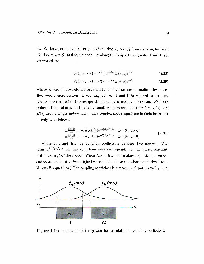
(mismatching) of the modes. When Kab — Kba = 0 in above equations, then ipa cind ipb are reduced to two original waves.( The above equations are derived from Maxwell’s equations.) The coupling coefficient is a measure of spatial overlapping
Figure 2.14: explanation of integration for calculation of corqDling coefficient.
Chapter 2. Theoretical Background 24
of normal modes over dielectric constant increments 6e in waveguide II as shown in Fig(2.14) cirid is calculated by the following integral;
Kab - c I f*Sefbdxdy JII (2.31)
where the integration range is cross section of waveguide II, and c is a constant related to the normalization of ·(/>„ and V’6· It is calculated that K^b — Kba-
2.6 Coupling Length And Power Transfer
Behavior of coupled waves can be determined by obtaining propagation constants of the waveguide system from the coupled mode equation. Two cases of propagation of two waves exist, codirectional and contradirectional. However, due to the fact that in our device we will utilize the codirectional propagation, we only consider this case {[da > 0,^t > 0). The coupled mode equations are then reduced to;
dA[z)dz
dB{z)dz
(2.32)
(2.33)
where Kab = Kla — i · positive vcilue) is set for simplicity. Byintroducing a new quantity 2A = fh — fda for convenience, and assuming the solutions for A{z) and B{z) to be in the form;
A{z) = (2.34)
B{z) = (2.35)
a quadratic equation for 7 is then obtained whose roots are;
7 = db\/A 2 +
Then the solutions are written as follows;
A{z) = — ¿Az
(2.36)
(2.37)
Chapter 2. Theoretical Background 25
B(z)KA,, K A . I +/'Az
(2.38)VA 2 + A 2 + a '
Then by using the above equations, the following can be derived;
?/, . ) = [/lee~' '= + (2..39)
y, ^) = i/)e'“ ' (2.40)
where the ratio of Ag and Bg is a j^ositive constant, and the ratio Ag and Bg is a negative constant. The following relations are also defined;
f^e — Pm + Pc
Po = P m - Pc
where;
Pm ={Pa + Pb) /3g = CIO + A2
(2.41)
(2.42)
(2.43)
uva vc^u ic lc s
II
(a)
oP«j __ Pft
2 ^
-P. Pc
P« (b) P.
ZJncoujylcd
coujplcd
Figure 2.15; Propagation constants in the case of codirectional coupling.
Equations (2.39,40) indicate that optical waves a. and i/’fc propagating along waveguides I and II are expressed by a linear combination of two waves
with the propagation constants Pe and Pg. Pg and /?o, therefore, ¿ire the propagation constants of the coupled mode system just described. As seen from
Chapter 2. Theoretical Background 26
EqLuitions(2.39,40), and Ao are constants determined by boundary conditions. When the boundary conditions are A(0) == 1 and .6(0) = 0 at = 0 (thcit is, when the wave is excited only at waveguide I), A(z) and B{z) are written as;
A{z) — e *^^(cos /3cZ + sin /3cz).APc
KB{z) =
He
(2.44)
(2.45)
since fa and /j are expressed by means of a normalized power flow, the power flow along waveguides I and II cire given by |yl(2)|^ and \B (z ) f respectively. Thus, the preceding equations can be written in a power form as follows;
|A(o)r
\B{z
l^(o)r
= 1 — Tsin'^ Pc
= Fsin^ PeZ
(2.46)
(2.47)
where F — Some calculated curves of Equations (2.46,47) arePc 1+ ( A ) - V > y
illustrated in Fig (2.16).
C % )-------- F = 1 . 0 ( J = 0 )------ F = 0.4(2l^0)
Figure 2.16; Power trairsfer between the coupled wciveguides.
Chapter 2. Theoretical Background 27
The power of waves propagating along the two guides vary or beat periodically. F means the maximum transfer of optical j^ower from the guide I to 11. The maximum i^ower transfer occurs at distance L, given as;
L = — 2fC
(2.48)
This Lc is called the coupling length. When the two modes are synchronized, tlnit is when fia = fdh·, F = 1 holds, and the coupling length is reduced to Lc — From this derivation, the following two important features are revealed; •
• When the two modes are synchronized, the coupling coefficient K influences only the coupling length, and a 100-percent power transfer is obtciined, regardless of K.
• When the two modes are not synchronized, a 100-percent power transfer can not be obtained cind is determined by the coupling coefficient and the
degree of synchronization.
Chcipter 2. Theoretical Background 28
2.7 Optical W aveguide D irectional Coupler
In an opticcil waveguide directional coupler where two identical singie-rnode 3-D waveguides are close to ecich other with a gap of only on the order of several wavelengths, 100-percent optical power is transferred, in principle, from one waveguide to the other. Using the directional coupler therefore, electro-optic modulation and switching with the high extinction ratio (defined as the ratio of the maximum and the minimum output levels) is possible. Consider a typical directional waveguide corp^ler, as the one shown in Fig(2.17), where fdy and ^2 are the propagation constants of the uncoupled waveguides and ¡3. and f3o are the propagation constants of the even and odd modes of the coupled waveguide system derived from the coupled mode theory. The guided mode incident from waveguide 1 excites the even and odd modes in phase with the same cunplitude at z = 0. The phcise shift between the even and odd modes become tt when the propagation distance L is;
Hence, at the output end of the coupling region, z = L, the resultant electric field distribution of the even and odd modes coincides with the electric field distribution of the guided mode in waveguide 2. In other words, all optical |)ower is fed into waveguide 2. L is defined as the coupling length, where 100-pcrcent
Figure 2.17: Operating principle of waveguide directioricil coupler.
Chapter 2. Theoretical Background 29
W a v e g u i d e s p a c i n g g j(L m )
a)W^W^4\T nt
W a v e g u id e s p a c i n g g m )
h)W^4\im, =3|i m
Figure 2.18: Variations of propagation constants of nornicil modes and the coupling coefficient with the waveguide spacing g. (a) Symmetrical (b) Asymmetrical directional couplers.
power is transferred if the two waveguides are identical. The power transfer
mechcinism is thus well understood by interference between the normal even and odd modes in the coupling region.
The projDagation constants ¡3e and ¡do are shown in Fig(2.18) against the waveguide spacing g lor a directional coupler. In a symmetrical directional coupler where W\ = W2 = if-mi and fdi — /32, considerable coupling occurs in the g < 8pm range. On the other hand, in a symmetrical directional coupler where wi = 4pm, W2 = ‘Spm and, hence, /3i > /?2, the coupling is not noticeable unless g is less than bpm. The power transfer due to the mode coui^ling is generally chciracterized by a phase mismatch {[3i — ^ 2) between the wiiveguides and the coupling coefficient K. Earlier the coupling coefficient was defined as;
K = - A) (2.50)
Therefore, K is easily evaluated by calculating the propcigation constants of the normal modes, on the basis of effective index method. Once K is specified, the directional waveguide coupler is analyzed based on the coupled mode
Chapter 2. Theoretical Background 30
2.8 B eam Propagation M ethod
Fiiicilly, we would like to point out to the beam propagation method, because it extensively used in our design via simulations of the structures we dealt with. Accurate analysis of guided-wave structures such as intersecting, branching and coupled waveguides is essential for the development of photonic integrated circuits. For such analysis, which could be quite involved and complicated, several different approaches have been d e v e lo p e d .T h e so called beam propagation method (BPM) has been successfully used to analyze a wide spectrum of guided- wave .structures. BPM is bcisically formed by approximate mathematiccil methods for solving problems of light propagation in dielectric optical waveguides of arbitrary shape. The method is only restricted by the conditions that reflected waves can be neglected and that all refractive index differences are small. With these restrictions, the waves described by the BPM can be regarded as cipproxiiTicite solutions for the scalar wave equation;
y·, z)k' ij) = 0 (2.51)
where ?/> describes an optical wave characterized by the free-spiice propagation constant k = ^ moving in a medium with the refractive index distribution n[x,y ,z). Also, even where analytical techniques are cvvailable, numerical techniques are often times employed to verify the designs before proceeding to invest serious effort in making new structures.
The most rigorous way of handling electromagnetic wave propagation in integrated optics is to solve the Maxwell’s equations with appropriate boundary
conditions. However, PIC structures hcive certain features which makes this approach very difficult to implement. The main reason is the large aspect ratio between the propagation distance and the transverse or hiteral dimensions of the propagating energy. The cross section may be contained in a few microns by a few microns wide window, but the propagation distance could be centimeters long. Therefore, to establish a fine enough grid for a boundary-value approach would pose a great challenge for computer memory and CPU performance.
Chapter 2. Theoretical Background 31
Fortunately, the guided waves in PIC’s have certain other properties which allow some approximations to be made. For example, in most cases the scalar wave equation is sufficient to describe the wave propagation. Secondly, the phase trouts of guided waves are nearly planar or their plane wave spectra are quite narrow. Therefore, they are paraxial. Thirdly, index changes along the propagation direction tend to be small and gradual in many situations. Hence, the wave amplitudes change slowly and back reflections are negligible in these Ccises. Under these conditions it is possible to reduce the scalar wave equation to the paraxial wave equation, which Ccin be written as;
d f _ d -‘f d-‘i,ZlkQl'lp „ Q 9 O 9oz ox^ oy^ + ko^[n'^(x,ij, z) — (2.52)
where ?г,. is a refractive index that describes the average phase velocity of the wave, and = E{z)U(x,y). That is, n,. determines the rcipidly varyingcomponent of the wave, and ?/> includes the slowly varying amplitude along the propagation direction. Thus for the polarization of interest, e(xpy,z) =
?/, The index ?2,. must be chosen as the index of the substrate.The paraxial wave equation describes an initial value problem as opposed to
a boundary value problem. As a result, one can start with an arbitrary initial wave amplitude, tf)(x,y,0), which could be a Gaussian beam formed by a lens, for example. The resulting amplitude A z away can be found by integrating the paraxial wave equation over Az. Repeating this procedure, one can find the evolution of the initial held profile over the waveguide. Note that one only needs the field at z = 0 in order to calculate the field values at z = Az. Therefore, there is no need to store or manipulate the field values at every grid point in the ^-direction as required in the solution of the boundary-value problems, thus it does not have cpu problems. Furthermore, all parts of the wave, including the guided and the radiation spectrum, are hcindled together.
The initial procedure for BPM involved operator techniques and FFT’s. Recently, however it has been shown that algorithms which are much more efficient cind robust can be generated by using finite-difference techniques.^'
Chapter 3
Design And Calculations
In this chapter we present the design considerations, calculations and the simulations for the Polarization Splitting Directional Couplers. As we have mentioned in the preceding chapter briefly, the coupler is basically a device of coupled waveguides. In directional couplers, two waveguides are brought in close proximity to each other and coupling of the guided modes propagating ¿dong the guides takes place. The directional coupler we designed hcive two symmetric strip-loaded rib waveguides and the coupling is codirectional.
In our design, we used unintentionally doped bulk GaAs/AlGaAs heterostructures grown on serni-insulating GaAs substrates by MBE. The wave-guiding tcikes place in the higher index GaAs core region and the confinement of the guided mode is done by the index difference of MBE grown layers in the vertical direction. The effective index difference caused by the rib geometry brings the confinement of the mode in the latercil direction under the rib. The use of the GaAs/ AlGaAs
material system was explained previously and is rnairdy due to the ultimate gocd of integration with other optoelectronic devices. The aluminium fraction X of the double heterostructure composition will determine the index difference between the layers and so is an important ¡parameter of design; the propagation
of the guided modes and the guiding will be effected by that parameter. Thus, the aluminium composition is a tuning pai’cirneter in our Ccdculations. Another important point is the single-mode operation of the device. Coupling mostly
32
Chapter 3. Design And Calculations 33
takes place in the straight section (coupling region) of the coupler in which the two guides are separated by a distance of only a few wavelengths of the light propagating through the guides. At the input and the output ports of the device, however, the waveguides should be separated by a distance large enough to have easy and efficient coupling to the fibers. We, therefore, used curved waveguides attached to the straight section of the guides both at the input and the output ports which separate the coupled waveguides. This, of course is an importcuit parameter that effects the device size. In fact all these parameters, the guide width the guide separation g (gap between the guides) in the coupling region, the bend radius R of the curved waveguides, the aluminium concentra.tion x of the material system are the parameters that we have dealt with to obtain a design yielding a single-mode, low-loss and compact device geometry leading to a Polarization Splitting Directional Coupler. The operation wavelength was chosen as A = i.hprn which is in the range for fiber optic telecommunications (A = 1.3 — f.6//?7r).
3.1 General Overview of Structure
in figure (3.1) our MBE grown double heterostructure used to fabricate the directional coupler is shown. The guided mode propagates in the core GaAs region. The core GaAs (higher index region) is stacked between two lower index
n=lAir
nAl Ga AsX l~xAl Ga AsX l-x
1 . 1
^GaAs GaAsA11Y
nAlGa^ AsX I’X Al Ga AsX l,x
A11\'/
” GoAs SI GaAs substrate
tc
Figure 3.1: MBE grown double heterostructure for Directioncil coupler
Chapter 3. Design And Calculations 34
AlxGui^xAs Iciyers and the entire structure is grown on an semi-insulating GaAs substrate. The thickness of the bottom cladding layer, djc, has to be large enough to prevent the guided mode to penetrate into the SI GaAs substrate region so as not to have losses in the substrate due to the overlapping of the substrate and the guided mode. The index difference between the vertically stacked layers is enough to confine a guided mode in the vertical direction (sirnihir to a slab waveguide). For lateral confinement of the guided mode, we have to etch a rib on the upper or top Al^Gai-^As cladding layer and obtain an effective index difference under the rib to confine the mode laterally.
In figure (3.2) we show a rib etched on the top cladding of the doubleheterostructure geometry. The rib height (or etch depth), h, the rib width, to, are important parameters that define guiding and will be important parameters in obtaining single-mode geometry. Becciuse the guides cire expected to be long, lithogra23hy and alignment requirements impose some limitations on the
rib width, w. Below 2pm, it is extremely difficult to align the mask and the sample for millimeter long structures. Furthermore, because we will use meted electrodes on the top of the guides, top of the ridge should be wide enough for at lecist 2pm wide electrodes. Considering that the chemical wet etching of the rib will result in an undercut, we Imve decided to use a 3pm wide stripes on the mask to define the waveguides. For our etch depth, this results in a rib geometry
as shown in figure (3.3).
Chcipter 3. Design And Calculations 35
-5 - 2(hltcin55) \x,m
\ 0 ! = 5 5
A\h
JL-u c i ------------------------------------------------------
Figure 3.3: Expected rib geometry after wet etch
Several considerations determine the optimum layer thicknesses in the heterostructures to be used for the directional coupler. The upper limit is determined by restrictions on the growth time and cost as well as the necessit}' of self depletion for low microwave and optical losses. The lower limit is set by the need tor an effective index contrast and the need to avoid the overlap of the guided field with the metal electrode, again to prevent losses.
3.2 The Coupler G eom etry
We begin the design of the coupler geometry by calculating the propagation constcints of the guided modes in the coupler geometry. The coupler we are designing, as presented in the preceeding section, is formed from lour layers of materials in vertical direction. The figure below shows the cross sectional schematic of the coupler (two coupled waveguides) in the coupling region ;
g — ----------------------1
II III IVs u b s tra te
Figure 3.4: Cross sectional view of the coupler in the coupling region
We utilize the effective index method to simplify the above structure. As seen in figure (3.4), we have five different regions where the regions 1, HI, V and
Chapter 3. Design And Calculations 36
the regions II and IV having the same vertical structure. We first calculate the effective indices of these five sections separately. These five effective indices will later be used to form a five Iciyer heterostructure in the x-direction. In regions I, III, and V, we, in-fact, have a four layer slab waveguide geometry, because the guided mode does not penetrate the substrate (sample is grown to meet this condition, i.e. the bottom cladding has a thickness ~ 1.8^?^г). Then regions I, III, and V will look like;
A i r n = l l a y e r 1
A l^ Gc^ ^ A s n i A ■ tY
l a y e r 2
G a A s ^ 2A
Vl a y e r 3
n j l a y e r 4
Figure 3.5: The structure which we solve for the regions I, III, and V.
In the regions II and IV, the guided mode does not penetrate in to the substrate and the metal cladding (the top cladding is designed to be thick enough for this purpose); and therefore the ciir as well. This fact simplifies the geometry a little further and we luive only a three layer slab geometry for these regions;
Al Ga AsX i - x layer 1
GaAs
Al As n.
dc layer 2
layer 3
Figure 3.6: The structure which we solve for the regions II, and IV.
To obtain the effective indices for all of these regions we only need to solve one from each group, because all the others in the same group are the scirne. We thus obtain an effective geometry that is now only one dirnensioricil and looks as shown in the figure (3.7).
This is now a five layer slab in the lateral direction. The fiiicil tcisk is to solve this five layer slab and find the guided modes and their propagation constants.
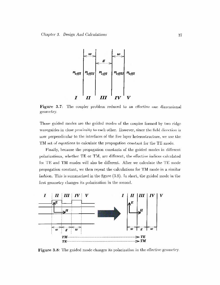
Chcipter 3. Design And Calculations 37
n·'^em
_ tv IV__ ^
g..... ¿5»
...................
^ e ff l
I I I I I I V
Figure 3.7: The coupler problem reduced to an effective one dimensional geometry.
Those guided modes are the guided modes of the coupler formed by two ridge waveguides in close proximity to each other. However, since the field direction is now perpendicular to the interfaces of the five layer heterostructure, we use the TM set of equations to calculate the propagation constant lor the TE mode.
Finally, because the ¡propagation constants of the guided modes in different polarizations, whether TE or TM, ai’e different, the effective indices calculated foi TE cuid TM modes will also be different. After we calculate the TE mode propagation constant, we then repeat the calculations for TM mode in a similar lashion. This is sumnnirized in the figure (3.8). In short, the guided mode in the first geometry changes its polarization in the second.
II \ III IV I VE
M
w g w
II.E
w
III
g
IV
w
TM ......... ......... .............. .................................... 73>TETE....................................................····............···>■ TAf
Figure 3.8 : The guided mode changes its polarization in the effective geometry.
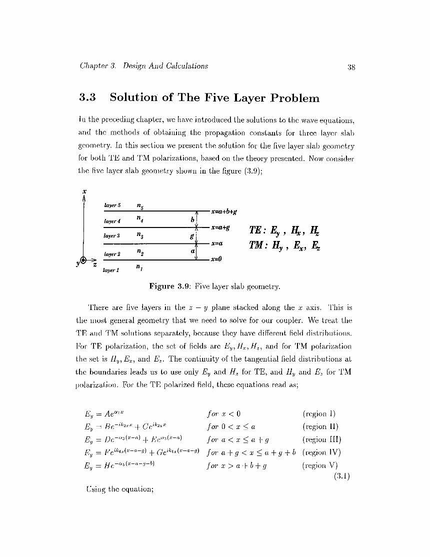
Chapter 3. Design And Calculations 38
3.3 Solution of The Five Layer Problem
In the preceding chapter, we have introduced the solutions to the wave equations, and the methods of obtaining the propagation constants for three layer slab geometry. In this section we present the solution for the live layer slab geometry for both TE and TM i^olarizations, biised on the theory ¡^resented. Now consider the five layer slab geometry shown in the figure (3.9);
X
klayer 5 « 5
layer 4
)b
\ x tt+b+g
layer 3 « 3T
____________i __
layer 2 a\( x=0
layer 1
T E : E y , H x , H ,
T M : Hy , E ^, Ez
Figure 3.9; Five Iciyer slab geometry.
There cire five layers in the z — y plane stacked along the x cixis. This is the most general geometry that we need to solve for our coupler. We treat the 3?E and TM solutions separately, because they have different field distributions. For TE polarization, the set of fields are Ey, H;,, and lor TM pohuization the set is Hy,Ex, cuid E^. The continuity of the tangential held distributions at the boundaries leads us to use only Ey and Hz for TE, and By and Eb tor TM pohirization. For the TE polarized held, these equations read as;
Ey for X < 0 (region 1)Ey = (j(^k2:,x Q ^ ,j. < (region 11)
Ey = -)- /_ 'e«3(.c-a) a < X < a -\- g (region III)
Ey - for a + g < x < a + g + h (region IV)
Using the equation;
fo r X > a + b + g (region V)(3.1)
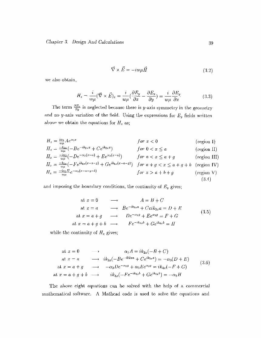
Chapter 3. Design And Calculations 39
V X E = —iiupH (3.2)
we also obtain,
H , = — (V X E), = — ( ^ wp, w p o x
i dEyo / - Q (3-3)OXJ top ox
The term ^ is neglected because there is ?/-axis symmetry in the geometry and no y-axis variation of the field. Using the expressions for Ey fields written above we obtain the equations for Hz as;
for re < 0 (region I)for 0 < x < a (region II)
= ^ ( - Z ) e - 3U·-«) + £!e«3U-a)) a < x < a + g (region III)
f or a + g < x < a + g + b (region IV)Hz -iarJI -as(x-a-(j-b)
tUf.L f or X > a + b + g
and imposing the boundary conditions, the continuity of Ey gives;
(region V) (3.4)
at X — 0 — >·at X = a — >
at X — a + g — »·at rc = a + ^ + 6 — i-
while the continuity of Hz gives;
A = B + C + Ceik2^a = D + E
D e - ^ ^ a E e ° ‘^a ^ p + G
^ — ik\xb _j_ ^^ik\xb _ JLJ
(3.5)
at X = 0 at X = a
at X = a + gat X = a + g + b
a iA — ik2x{—B -l· C) i k 2 x ( - B e - ^ ' ^ ^ ^ ^ + (76* 2.«,) ^ -«3(Z> + E )
—a ' iD e ~ ^ ^ a asEe^^^a = i k 4 x ( —E + G )
ik4x{—Fe~ ^ ' + — —aryH
(3.6)
The above eight equations can be solved with the help of a cornmercicil mathematical software. A Mcithcad code is used to solve the equations and
Chapter 3. Design And Calculations 40
obtain the roots that give reasonable values and do not diverge. The solution of the above equations is obtciined through the matrix equation below;
1 - 1 - 1 0 0 0 0 0 ^
0 g ’2 a' - 1 - 1 0 0 0
0 0 0 - 1 - 1 0
0 0 0 0 0 ^ik:\xb - 1
a y 2.1/ ~ i k 2 x 0 0 0 0 0
0 «3 — a s 0 0 0
0 0 0 t k ,\ x ^■ki\x 0
0 0 0 0 0 CVf) )
X = 0
Í a \BcD E F G
/
where the relations for the ¡Dropagation constants of the layers;
—cvi + /9 = ko^ny' = ky^+/3^ = k o W = k-2
(3.7)
- « 3 + 13' = ko^n ' = kG
kjyx T — k() Tii = k/{2 I /52 _ Í. 2 ^ 2 _ L 2
>-32
(3.8)
—as -\- (d — ko — k
give us all the unknowns in equation (3.7) except the propagation constant.The same analysis above ¿ipplies for the TM guided mode also. In this case
one starts with the TM set of fields, i/y, and T', , and cit the bounchiries one uses the continuity of the tangential fields IIy cind E^· Similar to that was done
Chapter 3. Design And Calculations 41
lor the TE mode, the equations for Hy in five different regions need be written and then by using the equation;
V X / / = iwcE
the ^-components of the electric field are obtained as;
1e ; -
iwe(V X vecH)
iwe^ dx
(3.9)
(3.10)
Following the same analysis and using the boundary conditions at the layer boundaries, the resulting equations are solved to obtain the propagation constant for the TM mode which appear as;
1 -1 -1 0 0 0 0 0 \0 g ik2xd -1 -1 0 0 00 0 0 £-«33 -1 -1 00 0 0 0 0 Q-ikixb -1«L
C2— i ’2.r
C2 0 0 0 0 00 -ihx -ik2n:a
£2ik2xC2 C3 C3 0 0 0
0 0 0 -cvaG3 C3 U
~2l4.TC4 00 0 0 0
! A0
\2 ¿4.1.“ 2 4 C4 C4
CV»)<-6 /
X = 0
B
cD E F G
\ H I(3.11)
(3.7) and (3.11) are the final equations to be solved for the coupler problem. As we stated before, these five layers of materials or the refractive indices of
Chapter 3. Design And Calculations 42
these five layers are in-fact the effective indices of the five different regions of the initial geometry. The indices and are the regions that have thesame initial configuration of materials; thus they have the same effective indices riejfi, which is formed by four layers with different refractive indices. And the indices ri2 and are the effective indices of the regions II and and IV that have the same material configuration, which is fonned by three layers with different indices. The calculation of the effective indices of these two different regions with three and four layers is necessary for both TE and TM polarizations, to be able to use them in the five layer coupler problem. In the preceding chapter the characteristic equations for the three layer slab problem for both TE cind TM polarizations was presented.
Now consider the three layer slab geometry below for regions II and IV of the initial coupler geometry;
A l .
Figure 3.10: Three layer slab geometry.
The normalized eigenvalue equation for the TE polarization for this geometry
(Equation 2.23) was;
V \ / i — b = tan s / 7— + tan N /----- - -f r\1 - 6 V1 - 6
2 _ „ 2
ГПЖ (3.12)
where a is the asymmetry parameter a = ¿uid 6 is the nornicilized index __< « 2 _ _ , TT- f f / Q ~r\2 - 7 7, 2.2 2 /------
6 =: ) a.nd V is the normalized thickness parameter V = kohynjAnd the normalized eigenvalue equation for the TM polarization for this shib geometry was (equation 2.25);
V V l — b = tan_^c +1 a + b _ ^ c + l b
------ \ ------- + tan ------ \ ------rc V l — 6 c — a \ 1 — b
+ ГПТГ (3.13)
where c is defined as c = —j- We have solved the above equations using aMathcad code, and ccilculated 6 (ue// from 6) for the TE and TM pohu’izations
Chapter 3. Design And Calculations 43
of a slab waveguide that have a thickness h, a substrate refractive index ?r.,, a guiding film index nf and a cladding layer index at the oiDeration wavelength A. The m = 0 yields the fundamental mode, m = L the first higher order mode, and etc. The four layer slab geometry has a solution similar to the solution of the five layer problem. A similar analysis yields the equation below for the four layer slab for TE mode;
11 12 13 14 15 1621 22 23 24 25 2631 32 33 34 35 3641 42 43 44 45 4651 52 53 54 55 5661 62 63 64 65 66
where the elements of the matrix are;
\ 1 a \Bc
XDE
/
16 = 0, 21
31 = 0, 32
= 0 (3.14)
= 0, 22 =
23 = 24 = -1 , 25 = -1 , 26 = ,34 ^ 35 ^ .36 = -1 , 41 = - i \ / l3 ‘ -
42 = 43 = _ ^ 2 44 = 0, 45 = 0, 46 = 0, 51 = 0,
52 = 53 = ^ ¿ 2 - 54 = - i ^ f p __
55 = 5g ^ ^ 52 = 0, 63 = 0, 64 =
65 = —i\Jl3‘ — 66 = —i"\/fd‘ ~(3.15)
and for TM mode the matrix elements of the above equation is modified as;
Chapter 3. Design And Calculations 44
11 1, 12 = - 1, 13 = -1 , 14 = 0, 15 = 0, 16 = 0, 21 = 0, 22 =
23 = 24 = -1 , 25 ^ -1 , 26 = 0, 31 = 0, 32 = 0, 33 = 0,34 ^ 35 ^ 36 = -1 , 41 = ^\/¡d '^ -
42 = 4-3 = 44 = 0, 45 = 0 , 46 = 0, 51 = 0,52 = 53 =
54 = - h \ 55 = :;^\/fd' - k-j , 56 = 0, 61 = 0, 62 = 0, 63 = 0,64 = ^ ^ ¡ 3 ^ - 65 =
QQ = - ^ ^ / f d ^ - h ‘(3.16)
3.4 A Sam ple Calculation
We will now present one of the calculations of several different geometries we did. As seen in the below figure, we have a number of parameters that cire to be optimized.
IItU=3]xm
■dl·t= 0 ,3 [ im
' dc~ 0· 6\am
4-' d, =2.8)im < be
h=0.7\dm
III
g
IV. w=3 ni^ ------------- >;
V
A ir
A l Ga^ A sX I ’X
GaAs
A l Ga^ A sX l - x
G aAs S I su b s tra te
x=0.3 y X =^l,55\im
Figure 3.11: Coupler geometry.
We chose the wavelength of the light we cire using ¿is 1.55/i?77. which is the wawelength of choice used in fiber optic telecommunications. The guiding region
Chapter 3. Design And Calculations 45
hcis a thickness of dcore = O.Gytun which is a reasonable number for guiding film thickness. The thickness of the bottom cladding layer dbc = l.Spm which is enough to prevent the guided mode overlapping with the SI substrate. We chose the value of the tojD cladding as h = 0.7pm to meet the necessciry requirements that cire presented previously. The parameters; w of the guide width, g of the gap between the guides, x the aliminiurn concentration and t of the etch depth cire the pcixarneters we oiDtimized. In this calculation we begin by choosing a guide width of 10 = 3/im, an etch depth of 0.4pm (t = 0.3pm) and made several ccilculations for different gaps g. The condition for the single mode operation should be met by our choice of geometries.
The index of refraction of the materials, depending on the matericils and the aluminium concentration x in ACGai-xAs is calculated using an empirical
formula;
(E, x ) = { l + 7 ( B / - Er“) + - H E / - V ) + 27B·' (3.17)
where E{eV) — 7 = 4Eo (Eo -eC) dependences of the Eq., Ed and£•'1' on the aluminium concentration x is as;
Eq{x) = 3.65 + 0 .871X T 0 . 179x 2
£rf(x) = 36.1 - 2.45x (3.18)£r(x) = 1.424 + 1.266X + 0.26x2
A few calculated refractive index values for different aluminium concentrations
X are presented below for A = l.hhpm·,
f o r X = 0 noaAs = 3.3769
f o r X = 0.25 nAloMGao.rsAs ~ 3.25 ( 3 . 19)
l o i X — 0.3 ' ^Alo. GciQ,' As 3 .22o
The calculations give the results below for the regions I and II ol the
Chapter 3. Design And Calculations 46
figure (3.11);
For region 1 (for the TE mode) ng/// = 3.3035273726 For region II (for the TE mode) Ueffn = 3.3079342389 For region I (for the TM mode) n^/// = 3.296618205 For region II (for the TM mode) neffii = 3.30424988
Now the two dimensional structure initially shown in figure (3.11) is reduced to five layer one dimensional problem, whose layers have the effective refractive indices calculated above is shown in the figure below;
n ^ f f l
w = 3
n e f f l l
S
n e f f i
i v = 3
I X e f f l l rxe f f i
Figure 3.12: Effective geometry of the coupler.
There are two guiding higher index regions in the above structure; these regions are II and IV. These are in-fact the regions of the initial structure defined under the rib with a ridge width of 3pm. The structure should be single rnoded; Guiding regions II and IV should guide only the fundemantal mode {rn = 0; single mode in the lateral direction). We can check and guarantee this by looking at the V parameter of the guides. As we presented in the previous chapter, the condition for single mode guiding is; V < tt. V = where nj isthe refractive index of the guiding film hiyer and Ug is the index of the cladding layers (this is a symmetric structure; the cladding at both sides have the same index of refrciction). In the above geometry ??./ = «ind rig — n-e///, andh is the guiding layer thickness(io, the guide thickness). By solving for V we obtain V = 2.07 < 7T for TE polarized guided mode, and V — 2.72 < tt lor TM polarized guided mode. So the structure above is a single-mode structure for both TE and TM polarizations. We can now solve the five hiyer problem using

Chapter 3. Design And Calculations 47
g(pm)33.544.5
1212.971547.581963.492513.27
17.35.682454.363490.654986.65
Table 3.1: sample calculcitios
the equations obtained in the previous section. But we should use the TE set of equations for five layer problem when the effective indexes calculated using TM calculations, and vice-versa. From the solution of the matrix equations for TE and TM, we get two non-vanishing solutions for the propagation constant of the structure (this final calculation gives the propagation constant of the guided mode in the coupler), /3\ and [ 2 ·, which correspond to the values of the even and odd modes. We determine which value belongs to which mode by text graphical methods (in-fact the higher value is the propagation constant of the even mode). We hcive calculated = 13.39833cm-^ and = 13.40092c?-n-‘ for g = 3pm for the TE mode in the above geometry. The coupling length of the guided TE
mode is then calculated by Lte = pevenEgoid·
3.5 R esults Of The Calculations
We have done several calculations for the coupling lengths of the TE cuid TM modes for the couplers that have different geometries. The parameters we have worked with are the etch depth h, (it is also characterized by t of the thickness remained at the top chidding after etch), x, the aluminium concentration in the alloy AlxGcii-xAs^ wciveguide width w, gap between the guides of the coupler g in the coupling region. The following are the results ol the calculations we have performed for the coupling lengths of the couplers with different parameters.
Chapter 3. Design And Calculations 48
g(Mnri)
Figure 3.13: TE, TM coupling lengths as function of coupler gap for ridge width w of 3/,i??2, aluminium cone. x=0.3, and the lateral clad, t of O.Spm.
Figure 3.14: T E , T M C o u p lin g L en g th s as fu n c tio n of co u p le r g ap for rid g ew id th w o f 3firn, a lu m in iu m cone. x = 0 .3 , a n d th e la te ra l ch id , t o f 0.2/.im.
Chapter 3. Design And Calculations 49
g (ij m )
Figure 3.15; TE, TM coupling lengths as function of coupler gap lor ridge width w of 2.5fJ,m, aluminium cone. x=0.25, and the lateral clad, t of 0.2/j,rn.
Figure 3.16: T E , T M co u p lin g le n g th s cis fu n c tio n o f co u p le r gevp for r id g e w id thw o f Z.hprn,, a lu m in iu m cone. x = 0 .2 5 , a n d th e la te ra l c lad , t o f 0.2/i?77,.
Chapter 3. Design And Calculations 50
Figure 3.17: TE, TM coupling lengths as function of coupler gap for ridge width w of 3pm, aluminium cone. x=0.25, and the lateral clad, t of 0.2p??r.
Figure 3.18: T E , T M co u p lin g le n g th s as fu n c tio n o f co u p le r gcip for r id g e w id thw o f 4 p m , a lu m in iu m cone. x = 0 .2 5 , ¿ind th e la te ra l c lad , t o f 0.2p?/7,.
Clmpter 3. Design And Calculations 51
Figure 3.19: TE, TM coupling lengths as function of hiteriil cladding thick, t for ridge width w of 3/j,m, aluminium cone. x=0.3, and the coupler gci.p g of 4.5;U??7..
Figure 3.20: T E , T M co u p lin g le n g th s as fu n c tio n o f r id g e w id th for c o u p le rg a p g o f 3^777, a lu m in iu m cone. x = 0 .2 5 , a n d th e la te ra l c lad , t o f 0.2/i'm .
Chapter 3. Design And Calculations 52
x(AI-fraction)
Figure 3.21: TE, TM coupling lengths as function of aluminium cone, x for ridge width w of coupler gap g of Spm, and the hiteral clad, t of 0.2/im.
Figure 3.22: Single-Multi mode regions depending on the Lateral Cladding thickness t vs. aluminium concentration x.
Chapter 3. Design And Calculations 53
3.6 O ptim um D esign
After the effective index nietliod calcufations and calculating the coupling lengths of the TE and TM guided inodes for different coupler geometries, we chose the optimum geometry. The calculations have shown that for x = 0.3, lu = 3.0/im, t = 0.3/,i??r and (j = 4.5/U777.(figure 3.f3), coupling lengths of the TE and TM modes are respectively 25f3.27/i?77 and 4986.65/im. The coupling length of the TM mode is nearly twice that of the TE mode = 1.98). This is the optimumgeometi'y that we find will separate the TE and TM modes at the output ports of the device. The choice of the length of the coupling region to be that of the TE coupling length, TE mode will couple to second guide while the TM will not, and if it is chosen as twice the TE coupling length, then the TE mode will couple back to the first guide while the TM mode will couple to the second guide; Two modes excited cit the same input port will be separated and leave the device from different output ports of the coupler.
■re··L™ = 2lI^
TM
TE,TM
-TE'.--TM" TE.
TE
Figure 3.23: Coupling of the TE and TM modes; one crosses over while the other is coupling back for our optimum coupler design.
As mentioned before, it was decided to use a wet etch process to define the optical guide ridge. The literature indicated that excellent wet etched guides could be made with the use of hard-baked photoresist as the etch mask. Preliminary empirical work showed that the fabrication toleriuice in ridge width
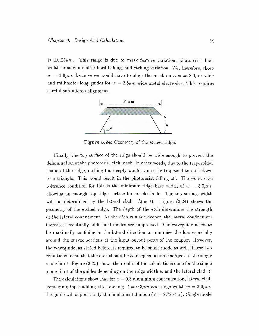
Chapter 3. Design And Calculations 54
is ±0.25firn. This I’cinge is due to mask feature variation, photoresist line- width broadening after hard-baking, and etching variation. We, therefore, chose w = d.Oprn, because we would have to align the mask on a lu — ‘i-Opm wide and millimeter long guides for tv = 2.5fmi wide metal electrodes. This requires ccireful sub-micron alignment.
3 |xm■X
Finally, the top surface of the ridge should be wide enough to prevent the delamination of the photoresist etch mask. In other words, due to the trcipezoidal shape of the ridge, etching too deeply would cause the trapezoid to etch down to a triangle. This would result in the photoresist falling off. The worst case tolerance condition for this is the minimum ridge base width of w = 3.Q/j,m, allowing an enough top ridge surface for an electrode. The top surface width will be determined by the lateral clad. h(or t). Figure (3.24) shows the geometry of the etched ridge. The depth of the etch determines the strength of the lateral confinement. As the etch is made deeper, the lateral conhnement increases; eventually additional modes are suppressed. The waveguide needs to be maximcilly confining in the lateral direction to minimize the loss especially around the curved sections at the input output ports of the coupler. However, the waveguide, as stated before, is required to be single mode as well. These two conditions mean that the etch should be as deep as possible subject to the single mode limit. Figure (3.25) shows the results of the calculations done for the single mode limit of the guides depending on the ridge width w and the lateral clad. t.
The calculations show that for x = 0.3 aluminium concentration, fiiteral clad, (remaining top cladding after etching) t — t).3pm and ridge width to = the guide will support only the fundamental mode [V = 2.72 < tt). Single mode
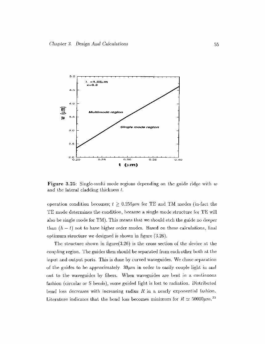
Clmpter 3. Design And Calculations 5.5
t (M-m)
Figure 3.25: Single-iriulti mode regions depending on the guide ridge with zv and the lateral cladding thickness Z.
operation condition becomes; t > 0.255/u?n for TE and TM modes (in-fact the TE mode determines the condition, because a single mode structure for TE will also be single mode for TM). This means that we should etch the guide no deeper thcin (h — t) not to have higher order modes. Based on these calculations, firicil optimum structure we designed is shown in figure (3.26).
The structure shown in figure(3.26) is the cross section of the device at the coupling region. The guides then should be .separated from each other both at the input and output ports. This is done by curved waveguides. We chose separation of the guides to be cipproximately 30gm in order to easily couple light in and out to the waveguides by fibers. When waveguides are bent in a continuous fcishion (circular or S-bends), some guided light is lost to I'cidiation. Distributed bend loss decreases with increasing radius R in a nearly exponenticd fa.shion. Literature indicates thcit the bend loss becomes minimum for R ~ 50000/ im.·*'*
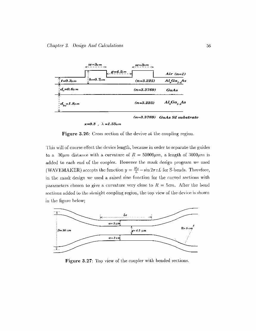
Chapter 3. Design And Calculations 56
\ t=0.3\xmX
t V = 3 } X t n<- --------->J?=4.5im K-- ^
h=0. TLimA /r - (n = l )
(rt—3,225) Al^Gcij^ A s
' d^=0.6lirnAl·
(n=3.3769) G aAs
' d,I be
(n=3.225)
(n=3.3769) G a A s S I substrate
x^O.3 у \ =l,55\int
Figure 3.26: Cross section of the clevive at the coupling region.
This will of course effect the device length, because in order to separate the guides to a 30fJ,m distance with curvature of R — 50000yum, a length of 3000/.im is added to each end of the coupler. However the mask design program we used (WAVEMAKER) accepts the function у = ^ — sm2'KzL for S-bends. Therefore, in the rncisk design we used a raised sine function for the curved sections with parameters chosen to give a curvature very close io R = hem. After the bend sections added to the straight coupling region, the top view of the device is shown
in the figure below;
Figure 3.27: Toj) view of the coupler with bended sections.
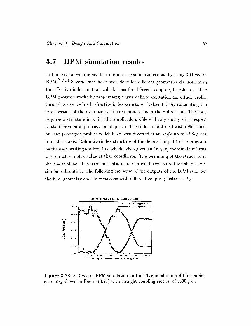
Chapter 3. Design And Calculations 57
3.7 B P M sim ulation results
In this section we present the results of the simulations done by using 3-D vector BPM. ' Several runs have been done for different geometries deduced from the effective index method calculations for different coupling lengths Lc- The BPM program works by propcigciting a user defined excitation amplitude profile through a user defined refractive index structure. It does this by calculating the cross-section of the excitation at incremental steps in the ^-direction. The code requires a structure in which the amplitude profile will vary slowly with respect to the incremental propagation step size. The code can not deal with reflections, but can proi^agate profiles which have been diverted at an angle iq? to 45 degrees from the .2-axis. Refractive index structure of the device is input to the program by the user, writing a subroutine which, when given an (x, y, z) coordinate returns the refractive index value at that coordinate. The beginning of the structure is the ,2 = 0 plane. The user must also define an excitation amplitude shape by a similar subroutine. The following are some of the outputs of the BPM runs for the final geometry cind its variations with different couj^ling distances
3D-VBRM (XE, L^=3300 pm)
Figure 3.28: 3-D v e c to r B P M s im u la tio n for th e T E g u id e d m o d e of th e coug e o m e try sh o w n in F ig u re (3 .27) w ith s tr a ig h t c o u p lin g se c tio n of 3300 pin.
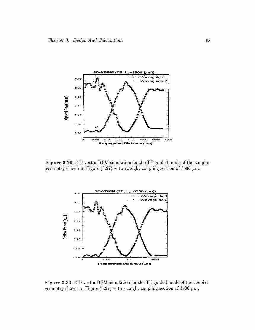
Chapter 3. Design And Calculations 58
3D-VBPM (XE, L„=3500 (M.m))
Figure 3.29: 3-D vector BPM simulation for the TE guided mode of the coupler geometry shown in Figure (3.27) with straight coupling section of 3500 prn.
Figure 3,30: 3-D v e c to r B P M s im u la tio n for th e T E g u id e d m o d e of th e c o u p le rg e o m e try sh o w n in F ig u re (3 .27) w ith s tr a ig h t co u p lin g se c tio n o f 3900 pm.
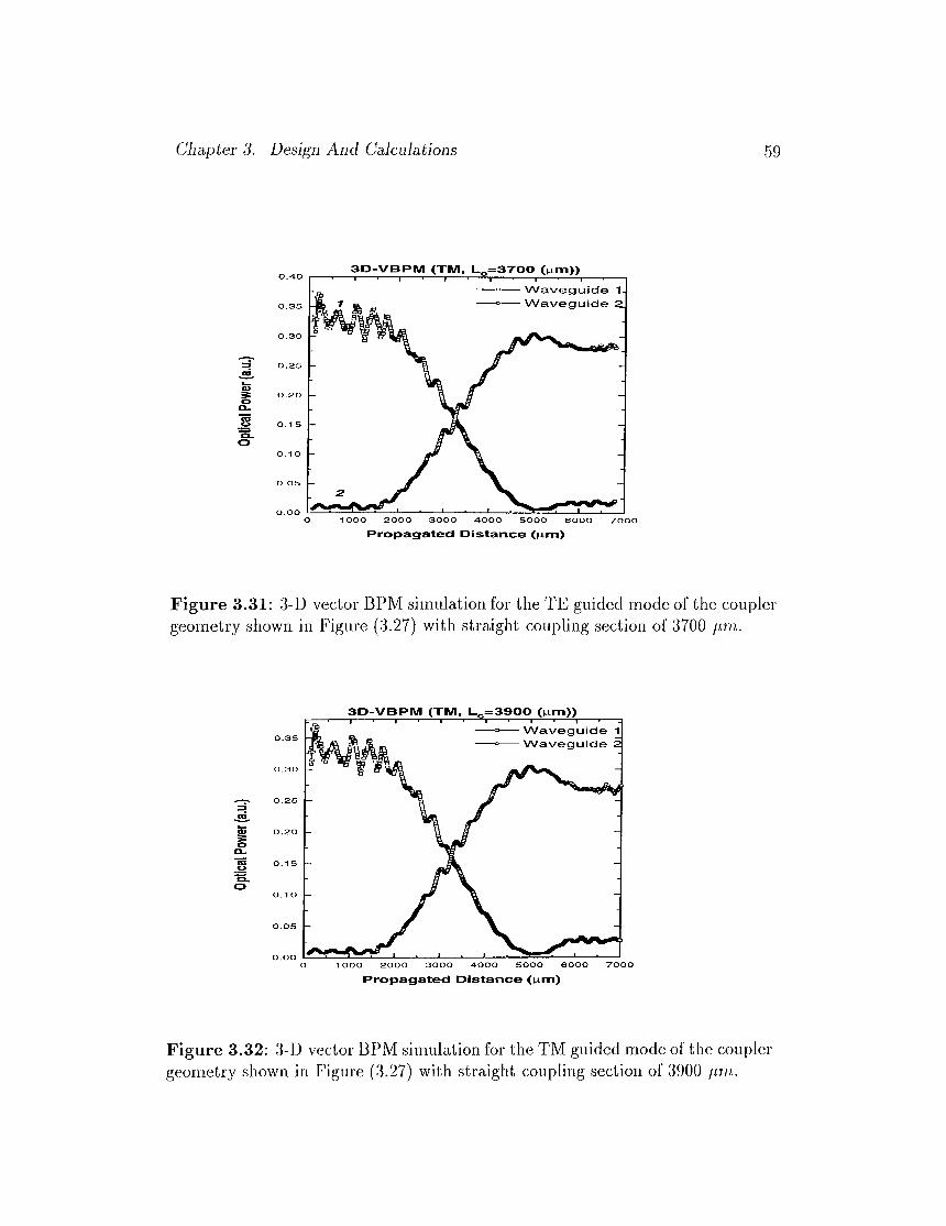
Chapter 3. Design And Caladations 59
Figure 3.31: 3-D vector BPM simulation for the TE guided mode of the coupler geometry shown in Figure (3.27) with straight coupling section of 3700 prn.
Figure 3.32: 3-D v e c to r B P M s im u la tio n for th e T M g u id e d m o d e o f th e c o u p le rg e o m e try sh o w n in F ig u re (3 .27) w ith sti'ciight co u p lin g se c tio n o f 3900 firn.
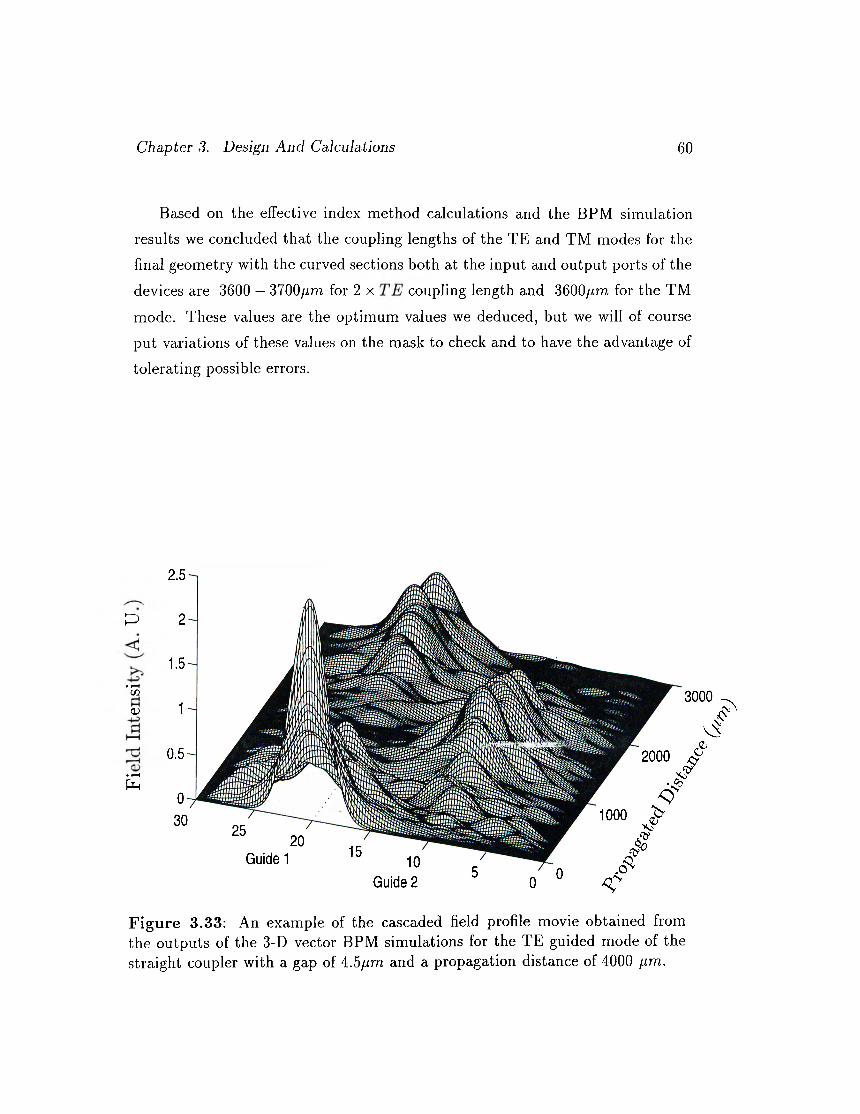
Chapter 3. Design And Calculations 60
Based on the effective index method calculations and the BPM simulation results we concluded that the coupling lengths of the TE and TM modes for the final geometry with the curved sections both at the input and output ports of the devices are 3600 — 3700/u.m for 2 x coupling length and 3600^im for the TM
mode. These values are the optimum values we deduced, but we will of course put variations of these values on the mask to check and to have the advantage of tolerating possible errors.
P
• i-HCOO)
• f— 1
P
Guide 1
F i g u r e 3 .3 3 : A n e x a m p le o f th e c a s c a d e d fie ld p ro file m o v ie o b ta in e d fro mth e o u tp u t s o f th e 3-D v e c to r B P M s im u la tio n s for th e T E g u id e d m o d e o f th es tr a ig h t c o u p le r w ith a g a p o f 4 .5 //m a n d a p ro p a g a t io n d is ta n c e o f 4000 pm.
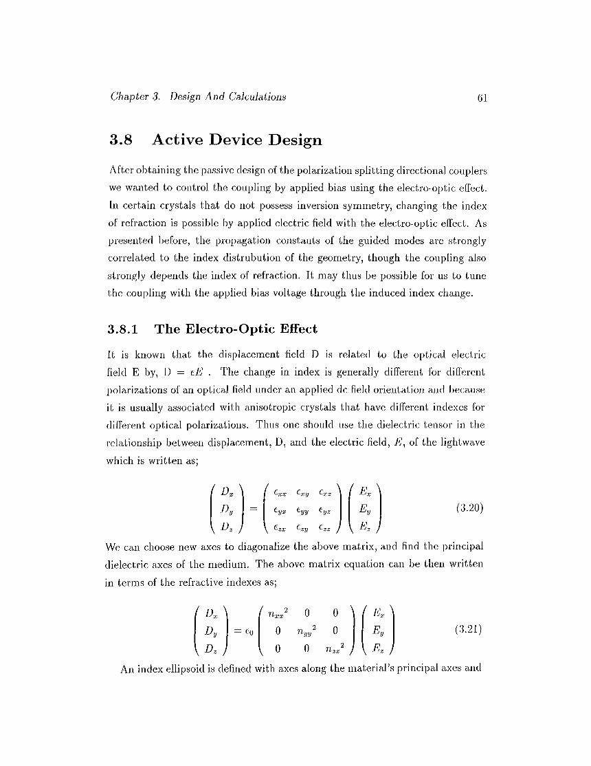
Chapter 3. Design And Calculations 61
3.8 A ctive D evice D esign
After obtaining the pcissive design of the polarization splitting directional couplers we wanted to control the coupling by applied bias using the electro-optic effect. In certain crystals that do not possess inversion symmetry, changing the index of refraction is ¡possible by a Dplied electric held with the electro-optic effect. As presented before, the propagation constants of the guided modes are strongly correlated to the index distrubution of the geometry, though the coupling also strongly depends the index of refraction. It may thus be possible for us to tune the coupling with the applied bias voltage through the induced index change.
3.8.1 T he E lectro-O ptic Effect
It is known that the displacement held D is related to the optical electric held E by, D = tE . The change in index is generally different for different polarizations of an optical field under an applied dc held orientation and because it is usually associated with anisotropic crystals that luive different indexes for different optical polarizations. Thus one should use the dielectric tensor in the relationship between displacement, D, and the electric field, E, of the lightwcive
which is written as;
i d ADyD, )
-XX xy \
yx yy yz\ zx ' zy
( E \■ x Ey
\ E . )
(3.20)
We can choose new axes to diagonalize the above matrix, and hnd the principal dielectric axes of the medium. The above matrix equation can be then written
in terms of the refractive indexes as;
D. \Dy
Dz )
— to
nXX0
0
0nyy
0
0
ru
I E^ ^Ey
\ Ez jJ(3.2f)
An index ellipsoid is defined with axes along the material’s principal axes and
Chapter 3. Design And Calculations 62
when the field is polarized along one of these directions, D will be parallel to E. In most materials at least two of these indexes are equal. These are called the ordinary index, while the third is called the extraordinary index. Materials with two extraordinary indexes are called biréfringent. In most semiconductor materials the index is isotropic when no additional DC or RF field is applied, and all of the indexes are same with no applied field. But this symmetry is broken when a bias is applied to the material.
Following the discussion of Coldren and Corzine the genaral index ellipsoid is defined as;
X+n. n + = 1
yy n. (.3.22)
Application of a field to an electro-optic material distorts this ellipsoid, so that generally off-diagonal terms appear in Equation (3.21). The electro-optic tensors are defined from the perturbation to each of the terms in the index ellipsoid.
That is;' ~ (3.23)= JlD jkEk
n uwhere r is the linear electro-optic tensor and Ek is the applied DC electric field. Three subscripts i, j, and k gives the relative orientations of the crystall axis, the optical electric field, and the DC electric field. Simplifying notation a little further; an abreviated notation is usually introduced, so that the three- dimensional tensor can be expressed in two dimensions. Using numbers from 1 to 6 for the first two subscripts, where 1 = xx, 2 = ?/?/, 3 = zz, 4 = yz., 5 = xz, and 6 = xy. The final subscript which refers to the applied DC or RF electric field orientation also is given a numerical subscript, where 1 = a;, 2 = y, 3 = Using these notations, the distorted index ellipsoid with the applied field becomes.
+ (4) + (-?) + 2(4) + (4) + (4) ^y = ' P-'·*·*)r i2 2 , 2 n r > ^ A n / r. ??/ ftr r 1 3
1' r C ' 4 t)
1_n^ ' 6
To determine the change in index for a propagating optical wave, we again must diagonalize the index matrix, or find the new principal axes for the distorted
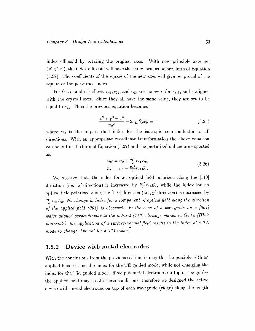
Chapter 3. Design And Calculations 63
index ellipsoid by rotating the original axes. With new principle axes set (x', y \ z')^ the index ellipsoid will have the same form as before, form of Equation (3.22). The coefhcients of the square of the new axes will give reciprocal of the square of the perturbed index.
For GaAs cind it’s cdloys, r4i,rs2, and res are non-zero for x, y, and z ciligned with the crystall axes. Since they all have the same value, they are set to be equal to ?’4i. Thus the previous equation becomes ;
x^ +no'
+ 2r4iE^xy = 1 (3.25)
where uq is the unperturbed index for the isotropic semiconductor in all directions. With an appropriate coordinate transformation the above equcition can be put in the form of Equation (3.22) and the perturbed indices are expected
as;1lx' — riQHyi = Uq — ^7'41jE ·
(3.26)
We observe that, the index for an optical field polarized along the [110]3
direction (i.e., a^'-direction) is increased by while the index for anoptical field polarized along the [110] direction (i.e., y'-direction) is decreased by
41 Ez- No change in index for a component of optical field along the direction of the applied field (001) is observed. In the case of a waveguide on a [001] wafer aligned perpendicular to the natural (110) cleavage planes in GaAs (IH-V materials), the application of a surface-normal field results in the index of a TE m,ode to change, but not for a TM mode.’
3.8.2 D evice w ith m etal electrodes
With the conclusions from the previous section, it may thus be possible with an applied bias to tune the index for the TE guided mode, while not changing the index for the TM guided mode. If we put metal electrodes on top ol the guides the applied field may create these conditions, therefore we designed the active device with metal electrodes on top of each waveguide (ridge) along the length
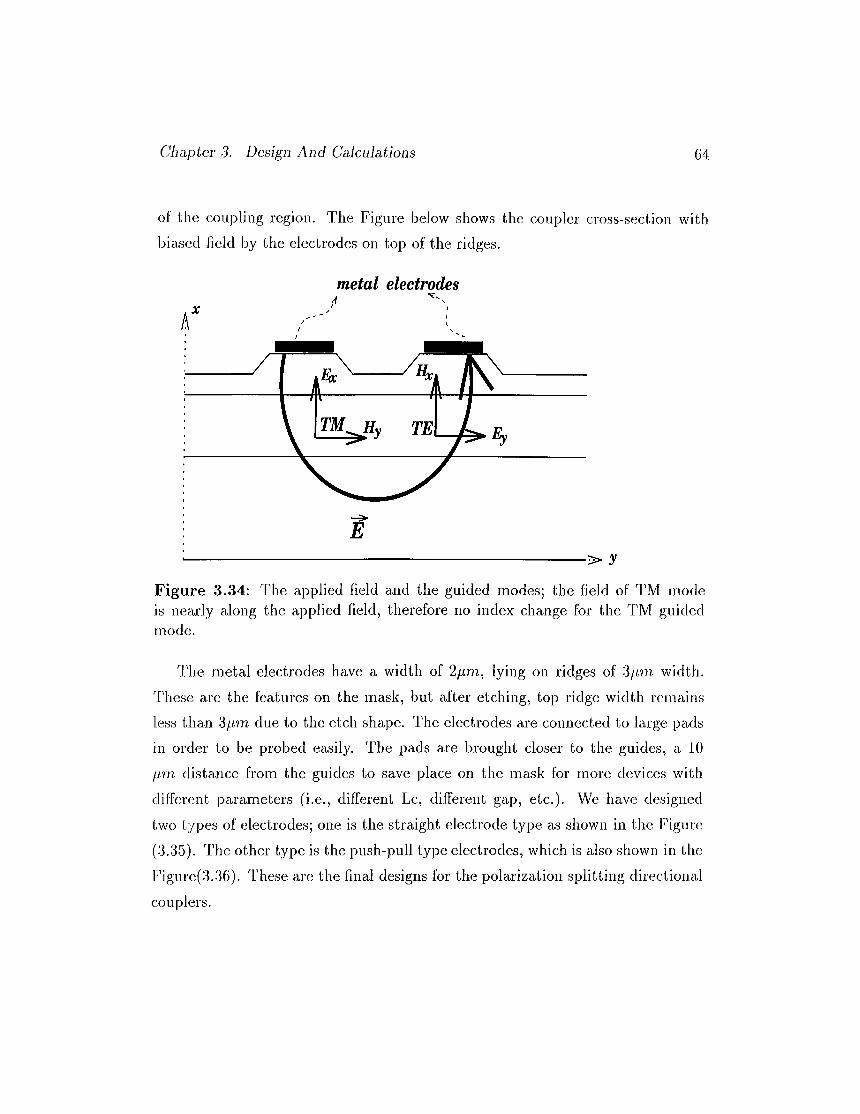
Chapter 3. Design And Calculations 64
of the coupling region. The Figure below shows the coupler cross-section with biased field by the electrodes on top of the ridges.
metal electrodes
Figure 3.34; The applied field and the guided inodes; the field of TM mode is nearly along the applied field, therefore no index change for the TM guided mode.
The metal electrodes have a width of 2jum, lying on ridges of 3fim width. These are the features on the mask, but after etching, top ridge width remains less than Sfim due to the etch shape. The electrodes are connected to large pads in order to be probed easily. The pads are brought closer to the guides, a 10 firn distance from the guides to save phice on the mask for more devices with different parameters (i.e., different Lc, different gap, etc.). We Imve designed two types of electrodes; one is the straight electrode type as shown in the Figure (3.35). The other type is the push-pull type electrodes, which is also shown in the Fhgure(3.36). These are the fiiicil designs for the polarization siDlitting directional couplers.
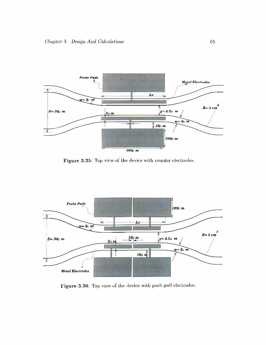
Clmpter 3. Design And Caladations 65
P ro b e P a d s | - v, -A.. : ■ ■
SO(pL m
Figure 3.35: Top view of the device with counter electrodes.
Figure 3.36: Top view of the device with push-pull electrodes.
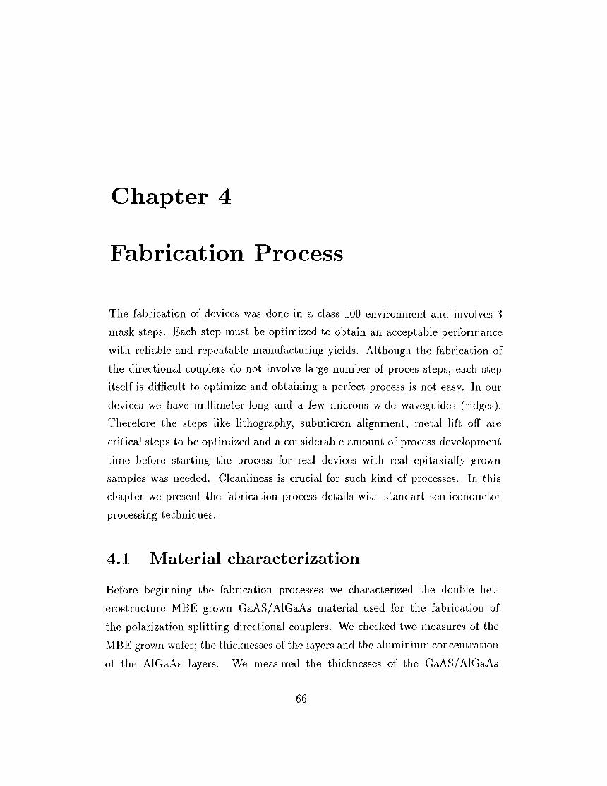
Chapter 4
Fabrication Process
The fabrication of devices was done in a class 100 environment and involves 3 mask steps. Each step must be optimized to obtain an acceptable performance
with reliable and repeatable manufacturing yields. Although the fabrication of the directional couplers do not involve large number of procès steps, each step itself is difficult to optimize and obtaining a perfect process is not easy. In our devices we have millimeter long and a few microns wide waveguides (ridges). Therefore the steps like lithography, submicron alignment, metal lift off are critical steps to be optimized and a considerable amount of process development
time before starting the process for real devices with real ej^itaxially grown samples was needed. Cleanliness is crucial for such kind of processes. In this chai^ter we present the fabrication process details with standart semiconductor processing techniques.
4.1 M aterial characterization
Before beginning the fabrication processes we characterized the double heterostructure MBE grown GaAS/AlGaAs material used for the fabrication of the polcirization splitting directional couplers. We checked two measures of the
MBE grown wafer; the thicknesses of the layers cind the aluminium concentration of the AlGaAs layers. We measured the thicknesses of the GaAS/AlGaAs
66
Chapter 4. Fabrication Process 67
layers by Scanning Electron Microscopy (SEM). The aluminium concentration is characterized by using optical spectroscopic methods.
4.1.1 T hickness m easurem ents
In our laboratory we hcive a JEOL 6400 Scanning Electron Microscope, cind the thicknesses of the GaAS/AlGaAs layers were measured by using it. The thicknesses of the MBE grown layers are important in terms of the operation of the fabricated devices from many point of views, and therefore effects the realization of our purposes. The coupling significantly depends on the effective indices of the coupler regions and therefore heavily depends on the layer thicknesses. Small pieces of samples cleaved from different regions of the wafer were mounted to the chamber of the SEM before illuminated by accelerated electron becuii. Both compositional and topographical pictures were taken and an example is shown in the Figure (4.1). We have measured the thikness of the top cladding hiyer to be around 5900-6000 A°, the core ciround 5800-6000 A°, and the bottom claddin layer around 17,000-18,000 A°. With these measurements it is observed that the top cladding layer is about 1000 A° less than the spec we designed. Moreover, we also observed the degrading of the MBE grown layer thicknesses towards the
Figure 4.1; SEM picture of the GaAs/AlGaAs double heterostructure.
Chapter 4. Fabrication Process 68
periphery of the wafer. Therefore a carefull planning of the samle cleaves were necessary to have maximum amount of efficient wafer area to process.
4.1.2 A lum inium com position characterization
Measurement of the A1 mole fraction in AlGaAs layers is important since compostional fluctuations may play crucial role in final device performance. Early detection of samples with specifications beyond acceptable tolerances may also save valuable process and test time. Several different techniques may be used to measure the composition of AlGaAs l a y e r s . W e used low temperature photoluminescence (PL)and Raman spectroscopy to determine the A1 mole fraction of the AlGaAs layers in our waveguide materials since optical chciracterization techniques are both realtively easy and nondestructive.
Low Temperature PL measurements
Photoluminescence measurements were done using a grating spectrometer with 0.4 rrieV resolution using a cooled GaAs photomultiplier and photon counting electronics. Samples were mounted stress-free on the cold finger of a closesd cycle cryostat and held held at 9±1 K. Since the changes in the bandgap with temperature at these temperatures is small, small temperature fluctucitions do not bring any measurable shifts in the peak positions. Total excitation powers as low as 5 rnW was used with a cylindirical focusing lens (f=20.0cm) to minimize power density and hence heating. 514.5 nm line of an Ar-fi laser was used as the excitation source. In Figure (4.2) and (4.3) we present the PI spectrum of both the GaAs and the AlGaAs heterolayers in our starting material. We use the energy of the excitonic recombination of GaAs as a calibration for the temperature of the Scuriple while the linewidth at half maximum (FWHM) is used as a measure of the quality of the GaAs layers. The peak energy of The FWHM of 1.48 ineV observed in this sample, while not the smallest value observed, is still within the range of values observed for high quality MBE grown GaAs. The PL spectrum of AlGaAs layer yields a sharp peak at 1.909 eV and a broader peak centered at
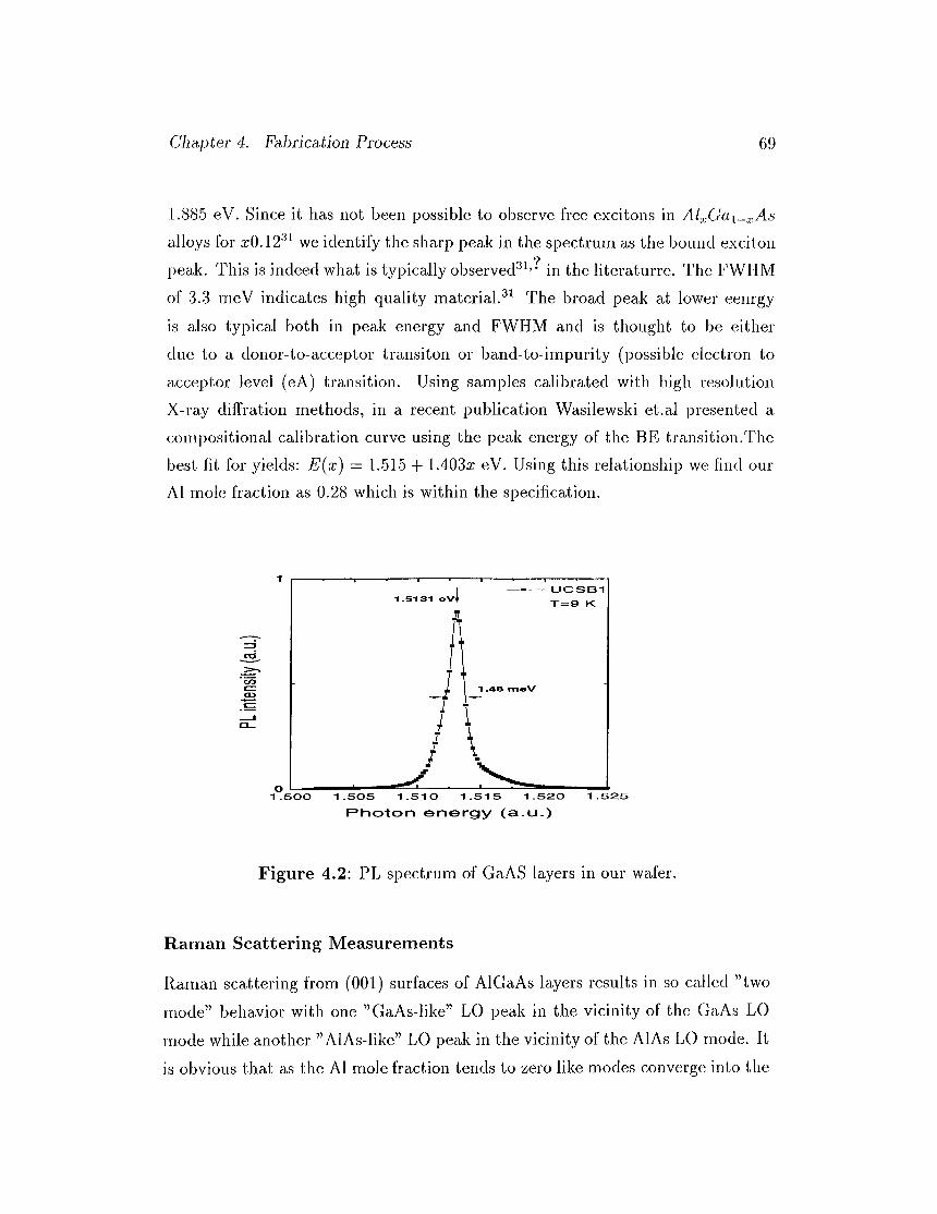
Chapter 4. Fabrication Process 69
1.885 eV. Since it has not been possible to observe free excitons in AlxGciy-xAs cilloys for a:0.12^ we identify the sharp peak in the spectrum as the bound exciton peak. This is indeed what is typically observed^^’· in the literaturre. The FWHM of 3.3 meV indicates high quality m a t e r i a l . T h e broad peak at lower eenrgy is also typical both in peak energy and FWHM and is thought to be either due to a donor-to-acceptor transiton or band-to-impurity (jDossible electron to acceptor level (eA) transition. Using samples calibrated with high resolution X-ray diffration methods, in a recent publication Wasilewski et.al presented a compositional calibration curve using the peak energy of the BE transition.The best fit for yields: E(x) = 1.515 + 1.403a; eV. Using this relationship we find our A1 mole fraction as 0.28 which is within the specification.
COcz
1.500 1.505 1.510 1.515 1.520 1.525
R h o t o n o n e r Q y ( a . u . )
Figure 4.2: PL spectrum of GaAS layers in our wafer.
Raman Scattering M easurements
Raman scattering from (001) surfaces of AlGaAs layers results in so called ’’two mode” behcwior with one ”GaAs-like” LO peak in the vicinity of the GaAs LO mode while another ”AlAs-like” LO peak in the vicinity of the AlAs LO mode. It is obvious that as the A1 mole fraction tends to zero like modes converge into
Chapter 4. Fabrication Process 70
C O
CO
1.84 1.88 1.92
Rhoton energy (eV)1 .96
Figure 4.3: PL spectrum of AlGaAS layers in our wafer.
’’parent modes”. It is thus possible to use both of the like modes to determine the A1 compositon of AlGaAs layers. To confim the PL results we performed Raman scattering measurements at room temperature in a quasi-backscattering configuration and LO allowed geometry using the 514.5 nm line of the Ar+ laser. The spectrum was calibartited with a NE lamp. The resulting spectrum for GaAS- like mode of AlGaAs and GaAs layers is shown in Figure (4.4). In addition to the LO mode of the GaAs layer we find a large peak at 279.7 С7П~ which is the GaAs-like mode of the AlGaAs layer. While not presented here, we also observed a much broader AlAs-like mode. However, due to the fact that AlAs-like peak is much broader which introduces significant errors in the determination of A1 mole fraction it was not used. The work by Wasilewski et.al. also provides the dispersion of the GaAs-like modes of AlGaAs where the GaAs-like LO frequency is realted to A1 compostion as : w(x) — 290.2 — 36.7æcm“ . Using this equation we infer the the A1 mole fraction as æ = 0.29 which confirms the results of the PL spectroscoiDy. Thus we conclude that MBE grown hétéroépitaxial material is both high qualtiy and has an A1 composition within a few percent of the intended
0.3.
Chapter 4. Fabrication Process 71
CCS
CCSc=' c oc=CCS£CCScx:
Frequency shift (1/cm)
Figure 4.4: Raman spectrum of GaAs ¿iiid AlGciAs hiyers.
4.2 P rocess D escription
4.2.1 C leaning A nd Sam ple Preparation
The wafers we are using are MBE grown 2” wafers. Due to the cost and difficulty of processing a whole wafer, and since the size of the patterns on the mask cire smaller, we cleave the original 2” diameter wafer and process the device on the pieces that are slightly larger than the size of the devices. We cleave the wafer into the pieces with a dicimond tipped scribing tool. Our structures on the miisk lies in a 1.1 cm by 1.2 cm rectangle, thus a carefull planning of the clecives is essential to yield these large, crystallographically oriented, rectangular samples from a
round wafer. Although the final cleaved sizes of the devices are 1.1 cm long, ¿m extra distance is needed on either ends of the devices to facilitate the final optical quality facet cleaves. Thus the samples we processed measure nearly 1.3 cm by1.3 cm. The samples must be cleaned carefully before processing to ensure best perforiricince. In our laboratory, we are using the standart three solvent cleaning procedure. First, after the cleave, it is usefull to blow the samples with N2 to remove the dusts remaining from the cleavage. The samples that will be processed
Chapter 4. Fabrication Process 72
are then immersed in boiling trichloroethane (TCA) bath for five minutes. After TCA bath, the samples are kept in a bath of room temperature acetone for five minutes. While in Acetone bath it was found that cleaning the sample surface with a clean coton tipped tool softly is usefull to remove all the residual materials and dirts. If it is done so slightly without scratching the surface of the sample, this mechanical brushing technique is very effective in removing the particles by overcoming the adhesive forces. The last chemical in which the samples are dipped in boiling Isopropanol (ISO). Again boiling in ISO bath should be for five minutes. At the end the samples were left in running (deionized) water (DI) for 3 minutes before they were dried by blowing continous N 2 with N 2 gun. After blowing water off with N 2 the samples were baked at 110 C° on a hot plate for two minutes. This baking is known as the dehydration bake and it evaporates all the water remained elfter N 2 blow.
It should be noted that while cleaning the wafer with three solvent cleaning process, the sample never should be allowed to dry before subsequent rinsing. If any solvent evaporates and dries on the surface, it would leave residues behind thcit may not be soluble in the subsequent solvent. Before the next process step, the samples should be cooled down for ten minutes after dehydration bake. The surface of the samples should then be viewed under opticcil microscope to observe the ceanliness of the sample surface. If observable dirts still exist on the surface, solvent cleaning may be repeated one more time. After cleaning the siimples ¿ire ready for the next process step.
4.2.2 P hotolithography
The lithography is the process of transferring the patterns of geometric shapes on a photomask to the photoresist material covering the surface of the sample.
By this process we can triinsfer the i^atterns on the mask. The machine we are using in our hiboratory for photolithography is a Karl Suss MJS3 mask aligner, with ultraviolet light at 365 nrn. For contact printing exposure We cire using AZ5214E as photoresist material in our processes, which is a positive photoresist
Chapter 4. Fabrication Process 73
with high resolution and high sensitivity. It is important to filter the photoresist before applying it to the surface of the sample. We use submicron filters with syringes to filter the resist. After placing the sample on to the spinner chuck, it is usefull to blow with N 2 . We have observed that the strong adhesion of the resist to the surface is very much important for our tiny and long patterns. The experiences showed that cipplying 100 7. HMDS, to improve the adhesion between the photoresist and the surface of the sample works very well. For this reason before applying photoresist to the sample, we cover the surface with HMDS and spin it at the same rate of the resist spinnig. Immediately after the HMDS spin, the surface of the sample is wholly covered with filtered photoresist. No bubbles should be left on the resist. We usually spin at 4000 rpm for 40 seconds to have a resist thickness of about 1.5 microns. Following the cipplication of the resist, samples cire soft baked at 110 C° for 50 seconds over a hot plate to remove the water and solvents that remain in the film after spin-on. After soft bake the samples should be cooled down for 10 minutes. Samples are then exposed under UV-lamp at 345 nm for 30 seconds. We use the constant intensity mode of the MJB3, and the optical power per unit area is 5 mW fcm^, so the total dose is typically 150 inJoulejarP. The orientation of the mask and the sample is also important. Because the etch shape depends on the crystallographic orientation of the sample, the guides must be aligned in the (011) direction on the sample to give the expected etch shape. While doing this orientation we also adjust the sample relative to the mask to avoid any remaining dirts that will ruin the lithography. It is essential to inspect every micrometer of the guides, because a small dirt on a guide will likely ruin the associated device. Finally, we use the
hard contact mode while doing exposure.
4.2.3 D evelopm ent
Development is the process step to dissolve and remove the resist from the regions that are exposed in the photolithography. The samples are developed in a solution AZ400 Developer, with the solution ratio as developer: H2O — 1:4, about
Chapter 4. Fabricatioa Process 74
seconds. The change in the color of the resist while developing gives a clue about the developing time, usually ten more seconds developing will be enough after the color change of the resist. The develoj^ed sample is then rinsed in running DI water to remove the photoresist and the developer residues. Firicilly again the samples are dried by N 2 gun gas flow. The patterns transferred on to the sample and the quality of the lithography is investigated using an optical microscope. If the resolution of the patterns are of good qualities, subsequent process steps are followed.
4.2 .4 R eactive Ion E tching (R IE)
In order to clean the surface of the sample before chemical wet etching process, RIE was used with the O2 plasma. This process is known as the oxygen ashing or oxygen plasma photoresist residue descum. The RIE machine we are using in our laboratory is a parallel plate leybold LE-301 Reactive Ion Etcher operating
at 13.56 MHz RF voltage. High vacuum is applied to the plasma chamber cind the pressure is lowered by turbo pumping down to few milibars. The patterned resist by photolithography should be post-baked before oxygen plasma ashing. Post-baking is done again on the hot plate for 50 seconds at 110 C°. The post- baked resist is then etched by RIE with the process data as follows; O2 flow: 20 seem, RF power: 51 W, Self Bias Voltage: 322 volts. Etching time: 120 seconds, total etched resist: 0.2 microns.
The application of the RIE cleans the photresist residues that should hcive been removed by development, and this enables us to have a uniform etch rate over the whole sample and improves the etch quality. Although it is very usefull to apply RIE before etching as a subsquent step after the lithography, it is observed that if metallization and lift off will be the next step after RIE, the lift off becomes
more difficult, because the RIE smooths the edges of the patterns. Taking this effect into account we performed RIE before metallization for only 1 minute.
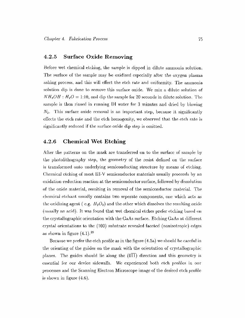
Chapter 4. Fabrication Process 75
4.2.5 Surface O xide R em oving
Beiore wet chemical etching, the sample is diiDped in dilute ammonia solution. The surface of the sample may be oxidized especially after the oxygen plasma ashing process, and this will effect the etch rate and uniformity. The ammonia solution dijD is done to remove this surface oxide. We mix a dilute solution of IVH4 OH : H 2O = 1:10, and dip the sample for 20 seconds in dilute solution, '['he sample is then rinsed in running DI water for 3 minutes and dried by blowing N 2 . This surface oxide removal is an important step, because it significantly effects the etch rcite and the etch homogenity, we observed that the etch rate is significantly reduced if the surface oxide dip step is omitted.
4.2.6 C hem ical W et E tching
After the patterns on the mask are transferred on to the surface of sample by the photolithography step, the geometry of the resist defined on the surface is transformed onto underlying semiconducting structure by means of etching. Chemical etching of most IITV semiconductor materials usually proceeds by an oxidation-reduction reaction at the semiconductor surface, followed by dissolution
of the oxide material, resulting in removal of the semiconductor material. The chemical etchant usually contains two seperate components, one which acts as the oxidizing cigent ( e.g. H2 O2 ) and the other which dissolves the resulting oxide (usually an acid). It was found that wet chemical etches prefer etching based on the crystallographic orientation with the GaAs surface. Etching GaAs at different crystal orientations to the (100) substrate revealed faceted (nonisotropic) edges
as shown in figure (4.1).^^Because we prefer the etch profile as in the figure (4.5a) we should be careful in
the orienting of the guides on the mask with the orientation of crystallographic planes. The guides should lie along the (Oil) direction and this geometry is essenticd for our device sidewalls. We experienced both etch profiles in our processes and the Sca.nning Electron Microscope image of the desired etch profile is shown in figure (4.6).
Chapter 4. Fabrication Process 76
Figure 4.5: Etch profiles for different crystall orientations.
Figure 4.6: Scanning Electron Microscope (SEM) picture of the etched ridge with the wright guide crystall orientation giving the desired etch shape and the lithographic photoresist on it.
We used an etchant of citric acid (CeHsOr) - hydrogen peroxide {H2O2 ). In this etchant system, the hydrogen peroxide is assumed to be the oxidizer, with the citric acid dissolving the resultant oxide material. The mixture is prepared in
the ratio of CeHsOr : H2O2 = 10:1. Etch rates of citric acid / hydrogen peroxide at room temperature for CaAs and A/o.sGno.TAs (on GaAs substrate) with no
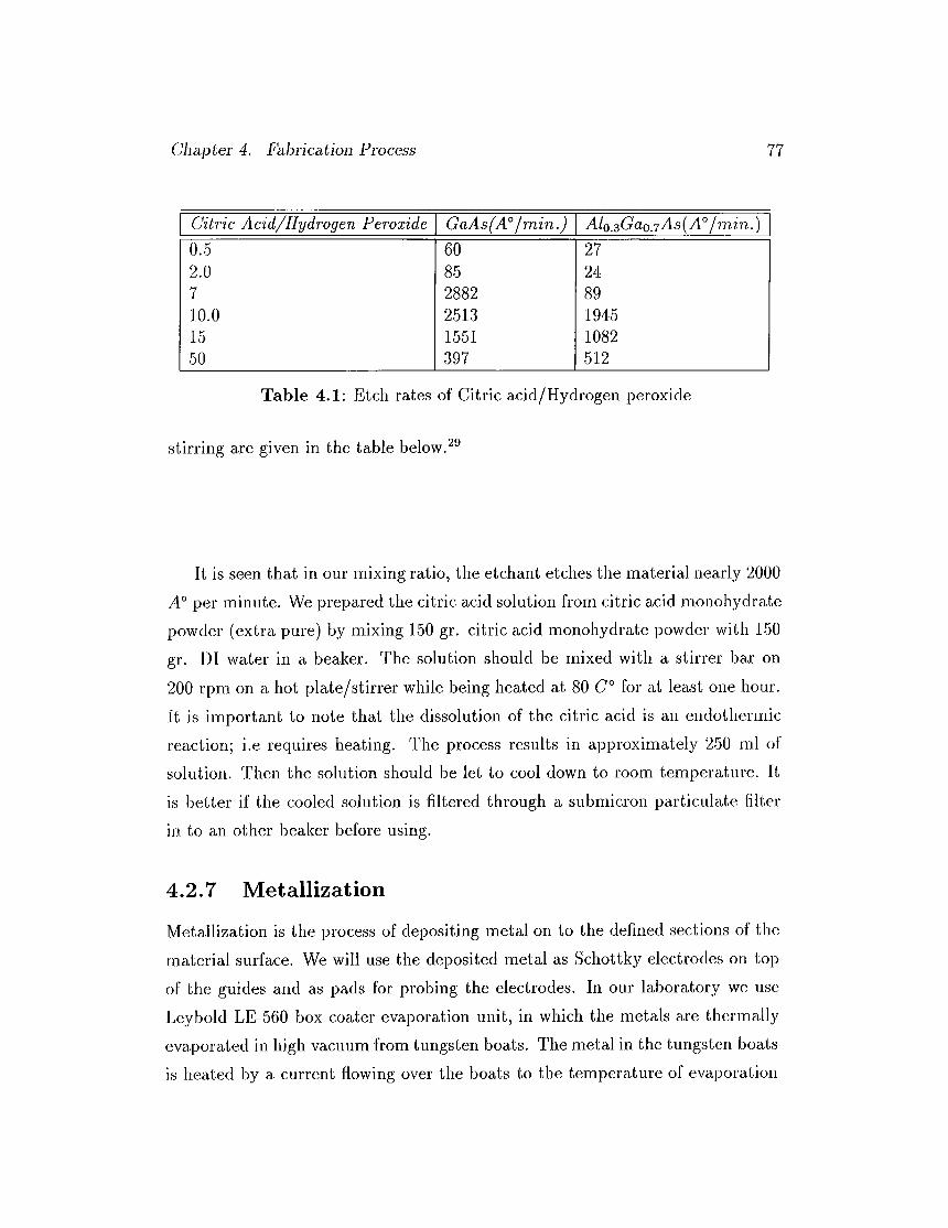
Chcipter 4. Fabrication Process 77
Citric Acid/Hydrogen Peroxide GaAs(A° fm in .) Alo,3Gao_rAs {A° / m in .)0.5 60 272.0 85 247 2882 8910.0 2513 194515 1551 108250 397 512
Table 4.1: Etch rates of Citric acid/Hydrogen peroxide
stirring are given in the table below.
It is seen that in our mixing ratio, the etchant etches the material nearly 2000 A° per minute. We prepared the citric acid solution from citric acid monohydrate powder (extra pure) by mixing 150 gr. citric acid monohydrate powder with 150 gr. DI water in a beaker. The solution should be mixed with a stirrer bar on 200 rpm on a hot plate/stirrer while being heated at 80 C° for at least one hour, ft is important to note that the dissolution of the citric acid is an endothermic reaction; i.e requires heating. The process results in approximately 250 ml of solution. Then the solution should be let to cool down to room temperature. It is better if the cooled solution is filtered through a submicron particulate fdter in to an other beaker before using.
4.2 .7 M etallization
Metallization is the process of depositing metal on to the defined sections of the material surface. We will use the deposited metal as Schottky electrodes on top of the guides and as pads for probing the electrodes. In our laboratory we use Leybold LE-560 box coater evaporation unit, in which the metals are thermally evciporated in high vacuum from tungsten boats. The metal in the tungsten boats is heated by a current flowing over the boats to the temperature of evaporation
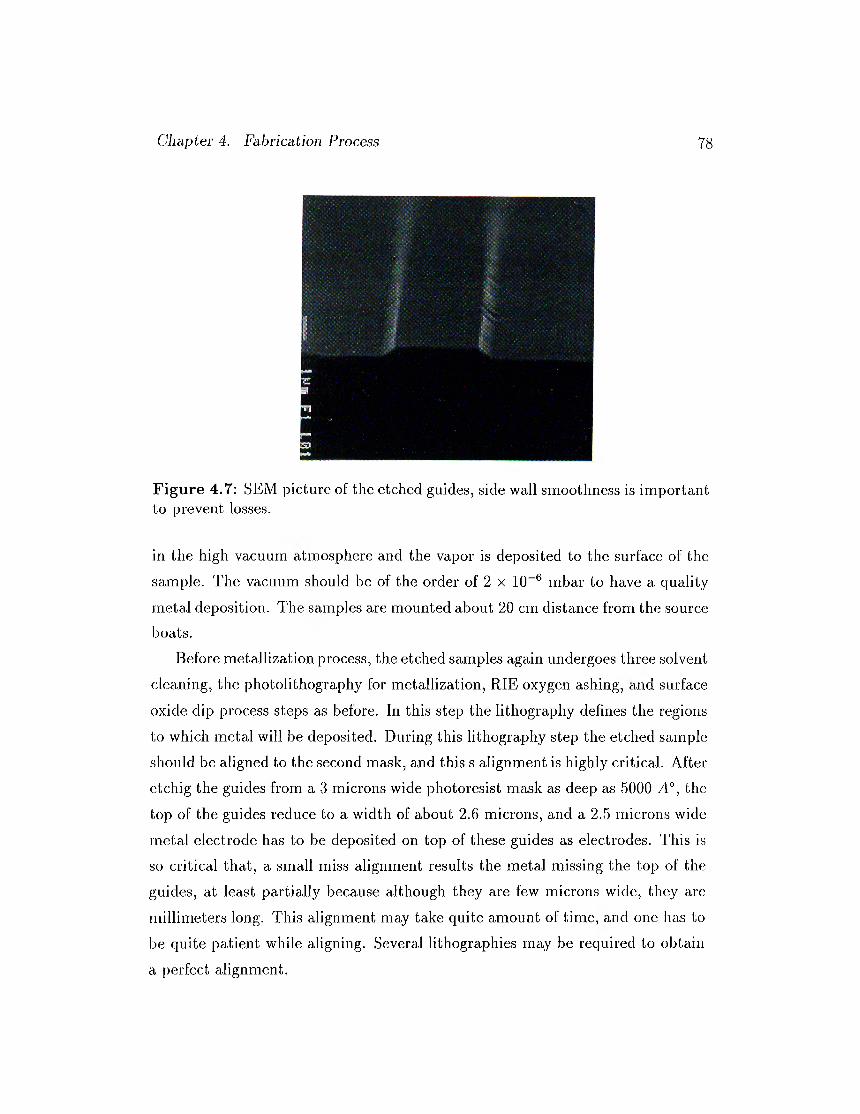
Clmpter 4. Fabrication Process 78
Figure 4.7: SEM picture of the etched guides, side wall smoothness is important to prevent losses.
in the high vacuum citmosphere and the vapor is deposited to the surface of the sample. The vacuum should be of the order of 2 x 10“® mbar to have a qiuility metal deposition. The scirnples are mounted about 20 cm distance from the source boats.
Before metallization process, the etched samples again undergoes three solvent cleaning, the photolithography for metallization, RIE oxygen ashing, cincl surface oxide dip process steps as before. In this step the lithography defines the regions to which metal will be deposited. During this lithography step the etched sample should be aligned to the second mask, and this s alignment is highly critical. After etchig the guides from a 3 microns wide photoresist mask as deep as 5000 A°, the top of the guides reduce to a width of about 2.6 microns, and a 2.5 microns wide metal electrode has to be deposited on top of these guides as electrodes. This is so critical that, a small miss alignment results the metal missing the top of the guides, at least partially because although they are few microns wide, they are millimeters long. This alignment may take quite amount of time, cind one luis to be quite patient while aligning. Several lithographies may be required to obtain
a perfect alignment.
Cimpter 4. Fabrication Process 79
Another important point is that; when a metallization process follows a photolithography process, it is usefull to generate resist with overhcinging edges (undercut). This will cause the thin metal film deposited from a point source to be discontinous over these edges. And this will make the lift off of the metal much more easier. To attain such kind of resist edges we apply tolueiie bath to the sample in a beaker just after the ultraviolet light exposure and before the development. The toluene hardens the surface of the resist and the underlying resist is softened by incomplete soft-baking. Although we consider that resist will not be developed if it is not exposed, it has some small development rate even if unexposed. By under-baking the resist during soft-bake step, the development rate of the unexposed regions in the depth increases whereas the resist surface is made harder and the development rate is lowered by applying toluene. At the edges the resist will have a dovetail shape which serves the discontinuity of the de2Dosited metal and easy lift off. A ten minute toluene soak is enough to harden about 0.2 microns of the upper surface of the resist. After toluene soak, the toluene is blowed off by N 2 and then developed as before. After mounting the sami^le into the evaporation unit we wait about 45 minutes to reach the Vcicuurn we need. In fact, 20-25 minutes is enough to reach the intended vacuum level, better results obtained when the vacuum was applied for more than 45 minutes. The thin titanimum layer is deposited first, before thick gold deposition. This
thin titanium deposition before gold sustains better adhesion between the surfcice of the sample and the deposited gold metal. We deposit about 2500 A° gold over 200 A° titanium on toj) of the guides as electrodes. The jDad metal is then made thicker by depositing a 5000 A° more. The following chart gives the relevcint
information of the metal we used in our processes.^®
The samples are left in acetone immediately after the metal deposition process. It may be usefull to use magnetic stirrer bar in acetone bath, preferably overnight.
One should be avare of the fact that acetone evaporates very quickly, therefore
Chapter 4. Fabrication Process 80
MaterialAll (Gold)Ti (titanium)
Melting Point(C°10621675
Density gjcm^19.34.5
Resistivity2.242.7
Table 4.2: Material properties
top of the beaker should be sealed with aluminium foil or a similar material. One should inspect the samples under the optical microscope while in acetone, and if there are any regions of metal did not lift off, should use syringe or squirt bottle. As a last resort, ultrasonic cleaning may be used to lift off the remaining metal, but this weakens the wafer, may even break it. During these lift off processes acetone should not be allowed dry on wafer. The samples are then washed with ISO with squirt bottle, then rinsed in running DI water for three minutes. The water on the sample is again dried with N 2 blowing.
4.3 M ask D esign and M ask Features
Masks, for the fabrication of the polarization splitting directional couplers in our laboratory, were designed by the software Wavemaker. While making the design with the wavemaker the granularity was set to the 0.1 pm. This was mainly because of the memory and cost problems. In our geometries we have curved sections, and drawing these curved sections with lower granularities recjuires quite high memories. Also it should be noted that the cost of the mask increases with lower granularity. After obtaining the optimum design; optimum gap, guide width (ridge with), coupling lengths Lc, the variations were also thought to be
put on to the mask to have a wide spectrum for tests. Thus, we designed several couplers with different parameters and put them on to the mask. Our process involves three mask steps; one is the mesa etch mask, second is the electrode and pad metallization mask and the third is the mask for the pads only to make the metal on the pads thicker. As was mentioned previously, the devices are about

Chapter 4. Fabrication Process 81
1.1 cm long, and because a large number of devices present downward, the total size of the first layer mask is about 1.1 x 1.2 cm^. The layout of the mask is shown in the Figure(4.12). Because the resolution of the features on the mask decreases on the periphery, we arranged the patterns to be at the central region of the mask as possible as the geometries and the sizes of the devices allowed.
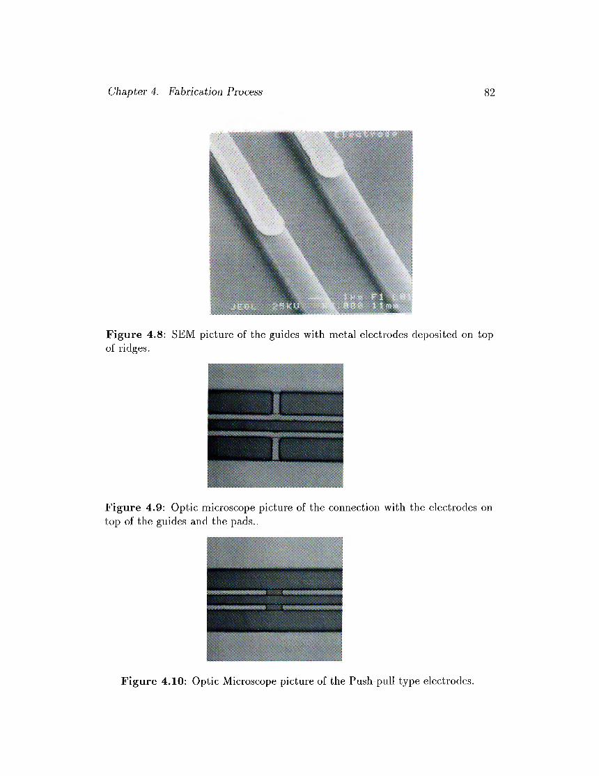
Chapter 4. Fabrication Process 82
Figure 4.8: SEM picture of the guides with metal electrodes deposited on top of ridges.
Figure 4.9: Optic microscope picture of the connection with the electrodes on top of the guides and the pads..
Figure 4.10: Optic Microscope picture of the Push-pull type electrodes.
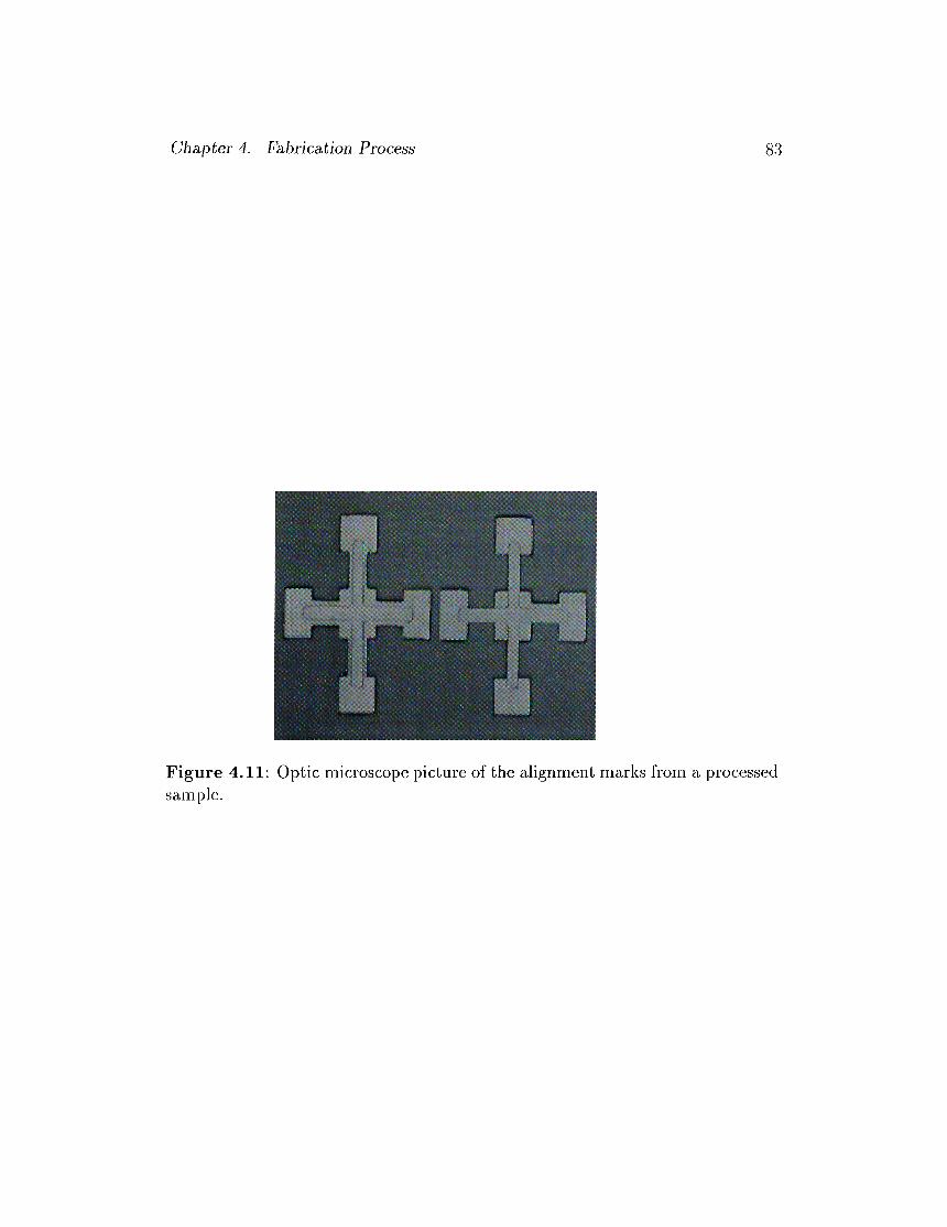
Clmpter 4. Fabrication Process 83
F igure 4.11: Optic microscope picture of the alignment marks from a processed sample.
Chapter 4. Fabrication Process 84
Figure 4.12: Mask layout; three layer mask with the layer 1 the guide etch mask, layer 2 the electrode metallization, and layer 3 the pad metal mask. The devices are in a 11,920 x 9,750 pirF mask area.
Chapter 4. Fabrication Process 85
An other important feature of the designed masks are the alignment marks. Because the alignment is critical in our processes, the cilignrnent miirks should be Lisefull to align the features on different masks. Therefore, we put these alignment marks on the mask at several j^ositions, especially at corners and the middle of the mask. The alignment marks we used are shown in the figures below.
2 0 ^ t t
g j u mI 10I__ .
60 lap
Figure 4.13: Marks for initial rough alignment
Figure 4.14: Marks for fine cilignment.
Chapter 4. Fabrication Process 8 6
DEVICES ON THE MASK | 1D evice # T y p e Lc (um) g (n m ) Electrode w (pim) Com m entsA Straight - - - 100B Straight - - - 100C Straight - - - 31 TE 2750 4.5 Push-Pull 32 TE 2750 4.5 Counter 33 TE 2250 4.5 PP 34 TE 2250 4.5 C 35 TE 2000 4.5 PP 36 TE 2000 4.5 C 37 TE 1750 4.5 PP 38 TE 1750 4.5 C 39 TE 1250 4.5 PP 310 TE 1250 4.5 C 311 TE 2750 4.25 PP 312 TE 2750 4.25 C 313 TE 2250 4.25 PP 314 TE 2250 4.25 C 315 TE 2000 4.25 PP 316 TE 2000 4.25 c 317 TE 1750 4.75 PP 318 TE 1750 4.75 c 319 TE 1250 4.75 PP 320 TE 1250 4.75 c 321 TE 2750 4.75 PP 322 TE 2750 4.75 c 323 TE 2250 4.75 PP 324 TE 2250 4.75 c 325 TE 2000 4.75 PP 326 TE 2000 4.75 c 327 TE 1750 4.75 PP 328 TE 1750 4.75 c 329 TE 1250 4.75 PP 3D Straight - - - 3E Straight - - - 10030 TM 3500 4.5 c 3.431 TM 3750 4.5 c 3.432 TM 4000 4.5 c 3.433 TE 2000 4.5 c 3.434 TE 2250 4.5 c 3.435 TE 2500 4.5 c 3.436 TM 4000 4.5 c 3 single arm37 TM 3750 4.5 c 3 single arm38 TM 3500 4.5 c 3 single arm39 TE 2500 4.5 c 3 Single arm
Figure 4.15: D e sc r ip tio n s o f th e d ev ices on th e m a sk .
Chapter 4. Fabrication Process 87
40 TE 2250 4.5 C 3 Single arm41 TE 2000 4.5 C 3 Single arm42 TM 4250 4.5 PP 343 TM 4250 4.5 c 344 TM 3750 4.5 PP 345 TM 3750 4.5 c 346 TM 3500 4.5 PP 347 TM 3500 4.5 c 348 TM 3250 4.5 PP 349 TM 3250 4.5 c 350 TM 2750 4.5 PP 351 TM 2750 4.5 c 352 TM 4250 4.25 PP 353 TM 4250 4.25 c 354 TM 3750 4.25 PP 355 TM 3750 4.25 c 356 TM 3500 4.25 PP 357 TM 3500 4.25 c 358 TM 3250 4.25 PP 359 TM 3250 4.25 c 360 TM 2750 4.25 PP 361 TM 2750 4.25 c 362 TM 4250 4.75 PP 363 TM 4250 4.75 c 364 TM 3750 4.75 PP 365 TM 3750 4.75 c 366 TM 3500 4.75 PP 367 TM 3500 4.75 c 368 TM 3250 4.75 PP 369 TM 3250 4.75 c 370 TM 2750 4.75 PP 371 TM 2750 4.75 c 3F TM 4000 - - 3G TM 3750 - - 3H TM 3500 - - 3 single arm1 TE 2500 - - 3 withoutJ TE 2250 - - 3 electrodesK TE 2000 - - 3L straight - - - 3M straight - - - 100
Figure 4.16: D e s c r ip tio n s o f th e d ev ices o n th e m a sk .
Chapter 5
R esults And Conclusions
In this chapter we present the results of the tests for the fabriccitecl GaAs/AlGciAs Polarizcition Splitting Directional Couplers, and discuss the conclusions of the present work and the suggestions for the future studies.
The fabricated devices, Polarization Splitting Couplers, were tested by using a fiber based experimental setup which is used for optical testing of the devices working at 1.55 ¡J,m. The samples were cleaved with optical quality facets from both ends of the sample (gold deposited markers were used to determine the cleavage points) before being mounted onto the test setup. The input light, from a thermo-electric cooler controlled DFB laser operating at 1.55 /.im, was coupled to the waveguides by an input lensed fiber. The polarization of the input light was controlled by a .3-loop liber polarization controller. Both the input and the output lensed fibers were fixed on xyz translation stages with ¡.im resolution in order to facilitate the positioning of the input and output fibers, to rnaintcdir an
efficient and easy coupling of light in and out the waveguides. The straight guides were used first to optimize the coupling by using a microscope objective at the output ports of the device. The output light from the microscope objective was collimated through a ¡rrojection lens and a polarizer onto an infrared camera. The mode shape of the output light was analyzed by a video analyzer and necessary optimizations were done by observing the mode shape before beginning the tests of the devices. After the optimization, the output light is again coupled in to a
8 8
Chapter 5. Results And Conclusions 89
lensed fiber and directed to a detector and an oscilloscope for measurements of oi:)tical power.
5.1 R esu lts for passive devices
The devices without metal electrodes on top of the guides are called the passive couplers. Before making the coupling measurements loss associcited with the guides have been measured. These losses include losses due to absorption , scattering and radiation. Absorption losses arise from imperfect material ti'cinsparency, while scattering and radiation (leakage) involve the transfer of optical energy from guided wave to non-guided radiation. Scattering arises from imperfect refractive index distributions (e.g., interface roughness), whereas leakage or radiation can occur even for ideally smooth structures, since it depends on the guiding capability of the designed and fabricated waveguide. Also there are losses arising from the coupling of light from fiber to guide and guide to fiber, which are called insertion losses. The loss measurements were done in strciight and curved waveguides by using the Fabry-Perot resoiicint cavity technique, obtained by tuning the wavelength of the laser via te m p e ra tu re .A distributed feedback laser (DFB) at the wavelength of 1.55 pm was used cis the light source. The temperature of the laser were controlled within ±0.1 using a Peltier cooler. Total propagation loss a (dB/cm) can be determined by using;a = 10 ) where K = L is the waveguide length and R. is the reflectivity of a cleaved facet, Tr and Ta are resonant maxima and antiresonant minima of the transmitted output power. We find that the average loss values for TE and TM modes, from the rneasuremnts through straight and curved guides, is about 2.6 dB/cm for the TE guided mode, and is about 5 dB/cm lor the TM mode. The losses increase with the curved sections and it is about 4 dB/cm for the TE mode for a coupler with straight section of 2000 yum, and 6.0 dB/cm for TM mode. These results are a bit slightly larger than 2.0 dB/crn for straight waveguides.
The results of the tests for coupling fractions of the guided modes are
Chapter 5. Results And Conclusions 90
presented below. The coupled fi'cictions were deduced by dividing the output power from the lower output port to the total power from the upper and lower ouput port of the couplers, if the light is injected to the upper input port. Typically, polarized light was injected at the upper input port and power from both output ports was measured seperately. The ratio of the power at the lower output port to the total power at the output ports is then used as a measure of coupling length. Since the purpose of the theoretical design was to split the TE and TM i^olarizations, we were expecting to extract the TE guided mode from the ui>per output port, while the TM guided mode leaves the device from the lower output port, if the light is input from the upper port. This is the case of the back-coupling of the TE mode cind the forward coupling of the TM mode. From the experimental data we estimate that the full coupling of the TE mode takes place when the straight coupled section of the couplers Lc is about 1500 firn Lc value for the TM mode is about 2250 pm. This corresponds to a ratio of
= 1.5. This value is below the desired value of 2.0. Examination of deltaLc·'LcTWwith gap widths of 4.25|Um, 4.5^m, and 4.75 pm show that Lr. TM
LcTW ratio ranges
between 1.4-1.6 for g=4.25 pm, 1.-4-1.5 for g=4.5 pm, and 1.6-1.7 for g=4.75 p7n, showing an increasing trend with increasing g value.
Incident Power Uncoupled Power
Coupled Power
Coupling Ratio = ■Coupled pwr.
Coupled pwr. + Uncoupled pwr.
Figure 5.1; Representative picture of the coupling ratio mecisurernents.
Chcipter 5. Results And Conclusions 91
Figure 5.2: The parameters of the fabricated passive devices.
g=4.5|-Lm, w=3M.m, PP.
Figure 5.3: Coupling fraction, Push Pull (PP.) elect., g—4.5/iirn, lo = 'iprn.
Oq P •-S o Ox hi O c OQ o 3 o CL· CD Ox ■l:: 3
Coup
led fr
actio
n (c
ouple
d pw
r/tot
al p
wr)
cfq* P •-S CD Ox C ic aq P o O o CD O O N Orq
Coup
led fr
actio
n (co
upled
pwr
/totai
pwr
)
o C-+
- 2 Ox CD C/D c c~s cn Q o CD O to
OT
to
aq i=: o ox C cm o O CL· O) c l-J cm to Cl 1::
r o
0 o
3 g
w
o o o
Coup
led F
racti
on (C
ouple
d pw
r/tot
al pw
r)
n---
-'---
-1---
-^
■ +
+■
H H
SmJ__________I__________L
1- ·
cm c CD Ox b o c c: i=3 cm o o CL·
CD C/3 cm Oi 3
r 0
fjj
r °
L· O
Coup
ling
Frac
tion
(coup
led p
wr/to
tal p
wr)
+N Cl r 3 CO V 3 0 m
H H
o c~t-
CD Oi CD Co C to O to Co
Chapter 5. Results And Conclusions 94
g=4-.25M.m, w=3M.m, PP.
Lc
Figure 5.8; Coupling fraction of modes for g=4.25/im and w — 3pm.
5.2 R esu lts from active devices
In this section we ¡^resent the results of the tests for the coupling lengths of the guided inodes under an applied bias. We know that the TM guided mode is not effected from the cipplied field since the field of the guided mode is parallel to the applied field as summarized in chapter four. Therefore, the applied field affects the TE guided mode as expected from the electro-optic effect. We observe that the cipplication of a bias reduces the coupling length of the TE guided mode. This reduction is proportinal to the applied field and the results show a consistent decrease in coupling length with the increasing applied field. Although the change in the index is small, the reflection of this index change to the coupling length is significant. The results show that, with a 30V applied bias it is possible to decrease the coupling length by almost 800pm. This enables us tuning the coupling length of the TE mode by the applied bias, a crucial factor for optimizing
the coupling length to reach the desired coupling fractions. The nicignitude of
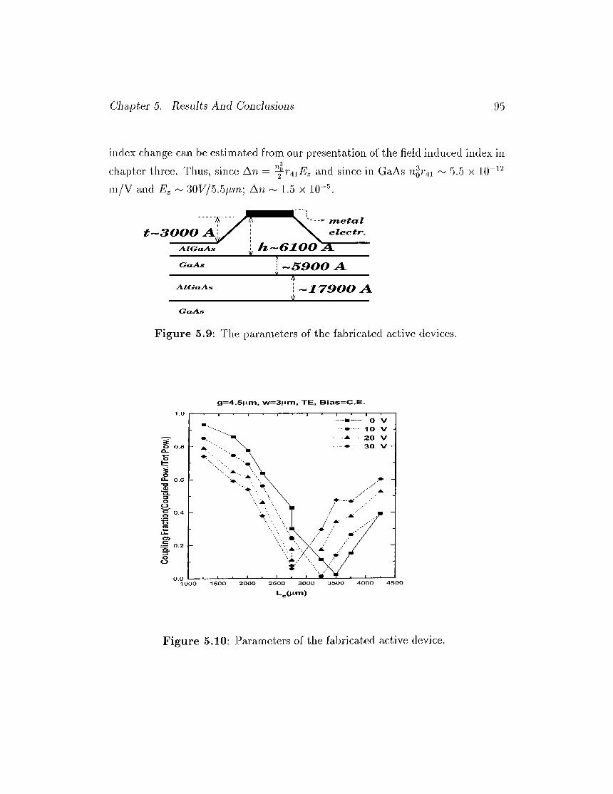
Chcipter 5. Results And Conclusions 95
index change Ccin be estimated from our presentation of the field induced index in3
chapter three. Thus, since A?v, = and since in GaAs ~ 5.5 x 10m/V and 30V/6.bjj,rri·, An ~ 1.5 x 10“' .
^-12
Figure 5.9: The pai’cimeters of the fabricated cictive devices.
g=4.5|Lun, w=3^uτı, TE, Bias=C.E.
L_(|xm)
Figure 5.10: Parameters of the fabricated active device.
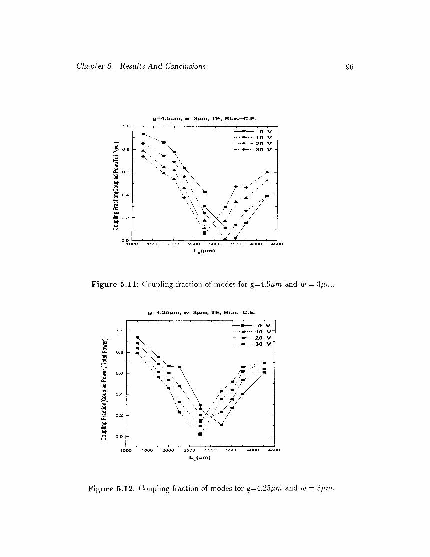
Chapter 5. Results And Conclusions 96
g=4.5|Lim, w=3|Lim, TE, Bias=C.E.
Figure 5.11; Coupling fraction of modes for g=4.5pm and w — 'ipm.
g=4.25|am, w=3ia.m, TE, Bias=C.E.
L c ( n m )
Figure 5.12: Coupling fraction of modes for g=4.25/;i7??- and to = ‘ipm .
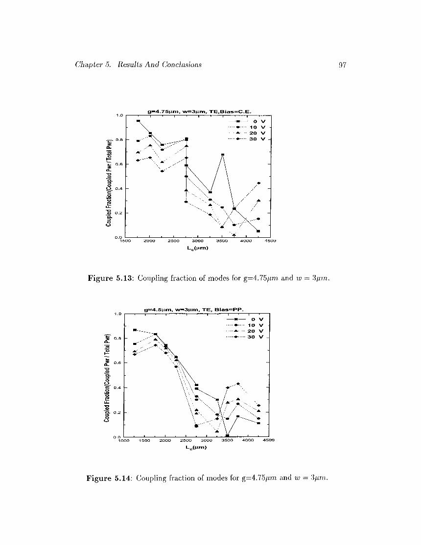
Chapter 5. Results And Conclusions 97
9=4.7510 1X1, w=3M'nn, TE,Bias=C.E.
Figure 5.13: Coupling fraction of modes for g=4.75^m and w = ‘¿/.irn.
g=4.5)Linn, w=3iLim, TE, Bias=PP.
Lc(um)
Figure 5.14: Coupling fraction of modes for g=4.75/r?7r and lu = -ipni.
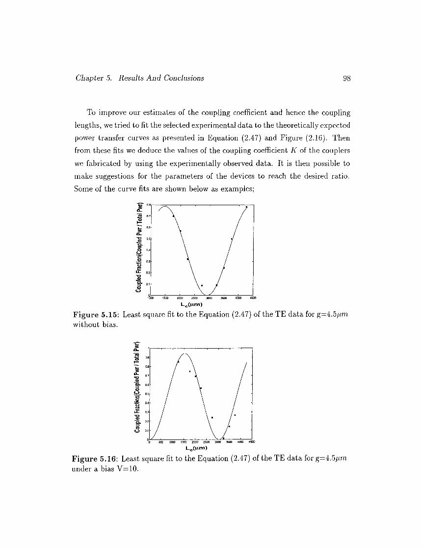
Chapter 5. Results And Conclusions 98
To improve our estimates of the coupling coefficient and hence the coupling lengths, we tried to fit the selected experimental data to the theoretically expected power transfer curves as presented in Equation (2.47) and Figure (2.16). Then from these fits we deduce the values of the coupling coefficient K of the couplers
we fabricated by using the experimentally observed data. It is then possible to make suggestions for the parameters of the devices to reach the desired ratio. Some of the curve fits are shown below as examples;
F igure 5.15: Least square fit to the Equation (2.47) of the TE data for g=4.5ytim without bias.
Figure 5.16: L e a s t s q u a re fit to th e E q u a t io n (2 .4 7 ) o f th e T E d a t a fo r g = 4 .5 /n n
u n d e r a b ia s V = 1 0 .
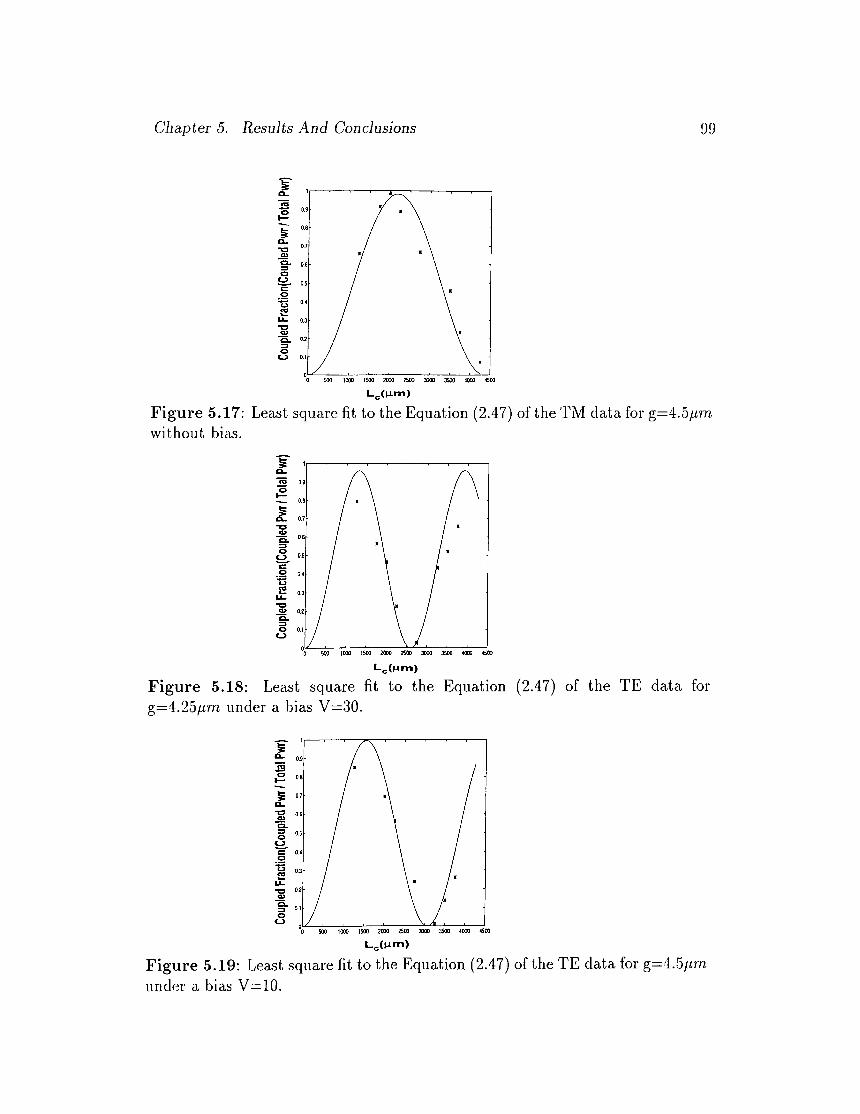
Chapter 5. Results And Conclusions 99
F igure 5.17: Least square fit to the Equation (2.47) of the TM data for g=4.5/im without bias.
F igu re 5.18: Least square fit to the Equation (2.47) of the TE data for g—4.25/mi under a bias V=30.
F i g u r e 5 .1 9 : L e a s t s q u a re fit to th e E q u a t io n (2 .4 7 ) o f th e T E d a t a fo r g=4.oprnu n d e r a b ia s V = 1 0 .
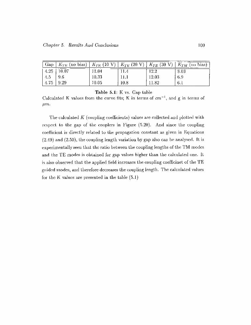
Chapter 5. Results And Conclusions 100
Gap K te (no bias) Kte (10 V) Kte (20 V) ^TE (30 V) K'TM (no bias)4.254.54.75
10.079.69.29
11.04 10..3310.05
11.411.110.8
12.212.0311.82
8.036.96.1
Table 5.1: K vs. Gap tableCalculated K values from the curve fits; K in terms of cm“\ and g in terms of pm.
The calculated K (coui^ling coefficients) values are collected and plotted with respect to the gap of the couplers in Figure (5.20). And since the coupling coefficient is directly related to the propagation constant as given in Equations (2.49) and (2.50), the coupling length variation by gap also can be airalysed. It is experimentally seen that the ratio between the coupling lengths of the TM modes and the TE modes is obtained for gap values higher than the calculated one. It is also observed that the applied field increases the coupling coefficinet of the TE guided modes, and therefore decreases the coupling length. The ccilculated values
for the K values are presented in the table (5.1)
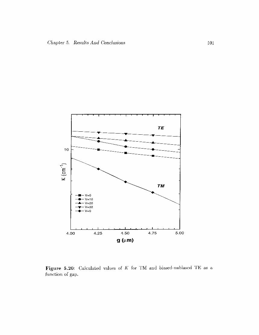
Chapter 5. Results And Conclusions 101
g (lim )
Figure 5.20: Calculated values of K lor TM and biased-unbiased TE as a function of g a p .
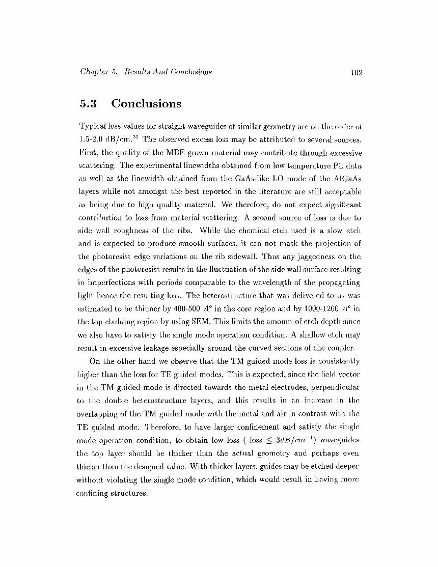
Chapter 5. Results And Conclusions 102
5.3 Conclusions
Typical loss values for straight waveguides of similar geometry are on the order of 1..5-2.0 dB/crn.^'^ The observed excess loss may be attributed to several sources. First, the quality of the MBE grown material may contribute through excessive scattering. The experimental linewidths obtained from low temperature PL data as well as the linewidth obtained from the GaAs-like LO mode of the AlGaAs layers while not amongst the best reported in the literature are still acceptable as being due to high quality material. We therefore, do not expect significant contribution to loss from material scattering. A second source of loss is due to side wall roughness of the ribs. While the chemical etch used is a slow etch and is expected to produce smooth surfaces, it can not mask the projection of the photoresist edge variations on the rib sidewall. Thus any jaggedness on the edges of the photoresist results in the fluctuation of the side wall surface resulting in imperfections with periods comparable to the wavelength of the propagciting light hence the resulting loss. The heterostructure that was delivered to us was estimated to be thinner by 400-500 A° in the core region and by 1000-1200 A° in the top cladding region by using SEM. This limits the amount of etch depth since
we also have to satisfy the single mode operation condition. A shallow etch may result in excessive leakage especially around the curved sections of the coupler.
On the other hand we observe that the TM guided mode loss is consistently higher than the loss for TE guided modes. This is expected, since the field vector in the TM guided mode is directed towards the metal electrodes, perpendicular to the double heterostructure layers, and this results in an increase in the
overlapping of the TM guided mode with the metal and air in contrast with the TE guided mode. Therefore, to have larger confinement and satisfy the single mode operation condition, to obtain low loss ( loss < 3dB/cm~^) waveguides the top layer should be thicker than the actual geometry and perluips even thicker than the designed value. With thicker layers, guides may be etched deeper without violating the single mode condition, which would result in hcwing more
confining structures.
Chcipter 5. Results And Conclusions 103
The coupling length ratio was found to increase as the gap width increases becoming as large as 1.6 for g=4.75 pm and only 20 % less than the desired value. Extrapolation of the data in Figure (5.20) shows that at slightly larger values of g—4.95 pm^ this ratio should I’each 2.0. Sevaral factors may contribute to lower than expected values of the coupling length ratio. First, due to uncertainties observed in layer thicknesses of the starting material, etch depths were kept conservative in order not to violate the single mode condition which may prove to be catastrophic. A simple effective index calculation shows that thicknesses of the remaining material, t, effects coupling length ratio significantly, in fact for t=0.35 pm we obtain = 1.6 which increases to 2.0 for t=0.3 pm and to 2.5 lor t=0.25 pm. Considering that most of our device had t-values above 0.3 pm, the results are understandable. Second, in order to keep the coupler geometry compact and short in length we opted for small value of g and hence shorter devices which results in smaller coupling length ratios. It seems that one should either increase g values to slightly larger values and hence accept longer coupler lengths or find other ways to adjust index differences to tune the ratio.
In conclusion, we have been able to demonstrate TE/TM polarizcition splitting in AlGaAs/GaAs alloy system with reasonably low loss. We have also shown thcit the coupling length of TE mode can be tuned with an cipplied bias. Further work needs to be done to reduce the loss as well as improve the coupling length ratio.

Bibliography
[1] R.C. Alferness, “Guided-wave devices for optical communication,” IEEE J. Quciiitum electron., vol. QE-17, pp. 946-959, (1981).
[2] A. Villeneuve, “Demonstration of all optical demultiplexing at 1555 nm with cui AlGaAs directional coupler,” Electron lett. , vol. 29, pjD. 721-722, (1993).
[3] A. Jajszczyk, “ Directional Coupler based planar concentrator networks,” Electron Lett., vol. 26, pp. 886-887, (1990).
[4] .J.C. Campbell, “ GaAs Electro-optic directional couplers,” Appl L. , vol.29, pp. 203-205, (1975).
[5] P. LIKamWa and A. Miller, “ 130 ps recovery of all-optical switching in GaAs multiquantum well directional coupler,” Appl. Phys. Lett. 58, (19),
[6] M. Sugimoto, “4 X 4 GaAs/AlGaAs optical Matrix Switches with uniform device clmrcicteristics using alternating electro-optic guided- wave directional couplers,” Journal of Lightwave Tech., vol. 9. No. 7, July
(1991).
[7] V.R. Chinni, T.C. Huang, “Performance of Field-Induced Directional Coupler Switches,” IEEE J. of Quantum Elect. Vol. 31, No. 11, Nov.
8] S.G. Lee, B.P. McGinnis, R. Jin, “ Subpicosecond Switching in a current injected GaAs/AlGaAs multiple-quantum-well nonlinear directional coupler,” Appl. Phys. Lett. 64 (4), 24 January (1994).
104
Bibliography 105
[9] R. Spickermann, G. Peters, N. Dagli, “A Polarization independent GaAs- AlGaAs Electrooptic Modulator,” IEEE J. of Quantum Elect., Vol. .32, No.5, May (1996).
[10] E.Garmire, “Semiconductor components for monolithic applications,” T. Tamil', Ed. New York: Springer-Verlag, (1985).
[11] S.Y.Wang, “GaAs travelling-wave plarization electro-optic waveguide modulator with bandwidth in excess of 20 GHz at 1.3 pm, ” Appl. Phys. Lett, vol. 51, pp. 8.3-85, (1987).
[12] T.H.Wood, “Multiple quantum well waveguide modulators,” J. Lightwave Tech., vol. 6, pp. 743-757. (1988).
[L3] R.J.Deri, E. Kapon, “Low-loss III-V semiconductor optical waveguides,” IEEE J. of Quantum Elect, vol. 27, No.3, march (1991).
[14] .I..1. Veselka, S.K. Korotky, “Optimization of T I LiNbO's optical waveguides and directional coupler switches for 1.56 pm wavelength,” IEEE .1. of Quantum Elect, vol. QE-22, pp.933-938, (1986).
[15] Reinhard Marz, “Integrated optics; Design and Modeling,” Artech House Inc. (1995).
[16] Hocker, G.B. and Burns, W.K., “Mode dispersion in diffused channel waveguides by the effective index method,” Applied Optics, Vol. 16, pp.ll3- 118, 1978.
[17] Yevick, D., and Hermanson, “Efficient beam propagating techniques,” IEEE .lournal of Quantum Elect. , Vol. 26, pp. 109-112, (1990).
[18] Huang, W. Chu S.T, “The Finite-difference Vector beam propiigation method; analysis cuid assessment,” IEEE Journal of Light Wave tech. , Vol. 10, pp. 295-305, (1992).
Bibliography 106
[19] Pregla, R., “MoL BPM - Method of lines based beam propagcition method,” Methods for modeling and simulation of optical guided-wave devices, Amsterdam, Elsevier, (1995).
[20] E.Kapon, R. Bhat, “Low-loss single mode GaAs/AlGaAs optical waveguides grown by organometallic vapor phase epitaxy,” Appl. Phys. Lett., vol. 50, pp.1628-1630, (1987).
[21] Wei-ping liuang, “Application of Finite-Difference Vector Beam Propagcition Method to Directional Coupler Devices,” IEEE J. of Quantum Elect, vol. 28, No.6, march (1992).
[22] E.A.J. Marcatili, “Dielectric rectangular waveguide and directioiicil coupler for integrated optics,” Bell Syst. Tech. J. 48, 2071-2102, (1969).
[2.3] Reinhard Marz, “Integrated optics; Design cind Modeling,” Artech House Inc. (1995).
[24] H. Nishihara, M. Plaruna, T. Suhara, “Optical Integrated circuits,” McGi’ciw Hill optical and Electro-optical Engineering Series, (1989).
[25] A.Bruce.Buckman, “Guided Wave Photonics,” Saunders College Publishing, (1992).
[26] A. Yariv, “Coupled-mode theory for guided-wave optics,” IEEE J. Quantum Elect., QE-9(9):919, sept., (1973).
[27] Y.Chung, N. Dagli, “An Assesment of Finite Difference Beam propiigation Method,” IEEE J. of Quantum Elect, vol. 26, No.8, march (1990).
[28] R. William, “Modern GaAs Processing Methods” Artech House, Boston,
279, (1990).
Gregory C. DeSalvo, Wen F. Tseng, and James Comas, “Etch rates and Selectivities of Citric Acid/Hydrogen Peroxide on GaAs, /I/o.sCVio.tAs, D o.'if-Tdo.sAs, 1 h q do.‘17A.s /?ro.524l/o.484l>s, and InP ,” .1. Electrochem.
Soc., Vol. 139, No. 3, March (1992).

Bihliography 107
[30] R. Wasilewski, M.M. Dion, D.J. Lockwood, P.Poole, R.W. Streater, J. SpringThorpe, “Composition of AlGaAs,” J. Appl. Phys. 81(4), pp. 1683- 1694, (1997).
[31] L. Pcivesi, M. Guzzi, “Photoluminescence of AlGaAs alloys,” .J. Appl. Phys. 75(10), pp. 4779-4842, (1994).
[32] N. Dagli, "private communication”
[33] Hiroaki Takeechu, “Low-loss single mode GaAS/AlGaAs miniature optical waveguides with straight and bending sections,” J. L. W. Tech. vol. 7, nO.7, pp. 1044, (1989).