Flatness ・ Light Point Defects - Sumitomo Electric...
2
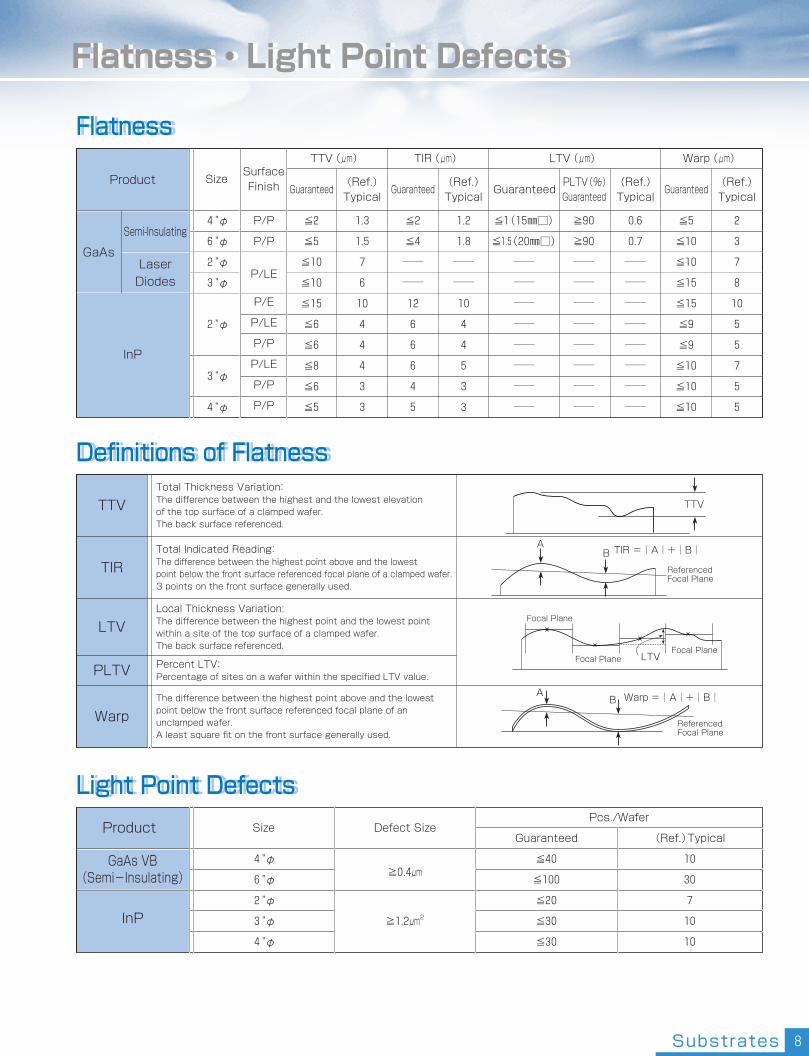
8 Substrates Flatness ・ Light Point Defects Flatness ・ Light Point Defects Flatness GaAs InP Product Laser Diodes Semi-Insulating Guaranteed (Ref.) Typical Guaranteed (Ref.) Typical Size ≦2 ≦5 ≦10 ≦10 ≦15 ≦6 ≦6 ≦8 ≦6 ≦5 4"φ 6"φ 2"φ 3"φ 2"φ 3"φ 4"φ 1.3 1.5 7 6 10 4 4 4 3 3 ≦5 ≦10 ≦10 ≦15 ≦15 ≦9 ≦9 ≦10 ≦10 ≦10 2 3 7 8 10 5 5 7 5 5 ≦2 ≦4 ____ ____ 12 6 6 6 4 5 1.2 1.8 ____ ____ 10 4 4 5 3 3 PLTV(%) Guaranteed (Ref.) Typical Guaranteed (Ref.) Typical ≧90 ≧90 ____ ____ ____ ____ ____ ____ ____ ____ Guaranteed ≦1(15㎜□) ≦ 1.5 (20㎜□) ____ ____ ____ ____ ____ ____ ____ ____ 0.6 0.7 ____ ____ ____ ____ ____ ____ ____ ____ Surface Finish P/P P/P P/LE P/E P/LE P/P P/LE P/P P/P Warp(μm) LTV(μm) TIR(μm) TTV(μm) Definitions of Flatness TTV TIR LTV PLTV Warp Total Thickness Variation: The difference between the highest and the lowest elevation of the top surface of a clamped wafer. The back surface referenced. Total Indicated Reading: The difference between the highest point above and the lowest point below the front surface referenced focal plane of a clamped wafer. 3 points on the front surface generally used. Local Thickness Variation: The difference between the highest point and the lowest point within a site of the top surface of a clamped wafer. The back surface referenced. Percent LTV: Percentage of sites on a wafer within the specified LTV value. The difference between the highest point above and the lowest point below the front surface referenced focal plane of an unclamped wafer. A least square fit on the front surface generally used. Light Point Defects Flatness Definitions of Flatness Light Point Defects Product InP GaAs VB (Semi-Insulating) Defect Size Size Guaranteed ≦40 ≦100 ≦20 ≦30 ≦30 (Ref.)Typical 10 30 7 10 10 ≧0.4 μm ≧1.2 μm 2 4"φ 6"φ 2"φ 3"φ 4"φ Pcs./Wafer TTV Referenced Focal Plane A B TIR =|A|+|B| LTV Focal Plane Focal Plane Focal Plane Referenced Focal Plane A B Warp =|A|+|B|
-
Upload
nguyenphuc -
Category
Documents
-
view
229 -
download
3
Transcript of Flatness ・ Light Point Defects - Sumitomo Electric...
8 Substrates
Flatness ・ Light Point DefectsFlatness ・ Light Point Defects
Flatness
GaAs
InP
Product
Laser
Diodes
Semi-Insulating
Guaranteed(Ref.) Typical
Guaranteed(Ref.) Typical
Size
≦2
≦5
≦10
≦10
≦15
≦6
≦6
≦8
≦6
≦5
4"φ
6"φ
2"φ
3"φ
2"φ
3"φ
4"φ
1.3
1.5
7
6
10
4
4
4
3
3
≦5
≦10
≦10
≦15
≦15
≦9
≦9
≦10
≦10
≦10
2
3
7
8
10
5
5
7
5
5
≦2
≦4 ____
____
12
6
6
6
4
5
1.2
1.8 ____
____
10
4
4
5
3
3
PLTV(%) Guaranteed
(Ref.) Typical
Guaranteed(Ref.) Typical
≧90
≧90 ____
____
____
____
____
____
____
____
Guaranteed
≦1(15㎜□)
≦1.5(20㎜□) ____
____
____
____
____
____
____
____
0.6
0.7 ____
____
____
____
____
____
____
____
Surface Finish
P/P
P/P
P/LE
P/E
P/LE
P/P
P/LE
P/P
P/P
Warp(μm) LTV(μm) TIR(μm) TTV(μm)
Definitions of Flatness
TTV
TIR
LTV
PLTV
Warp
Total Thickness Variation: The difference between the highest and the lowest elevation of the top surface of a clamped wafer. The back surface referenced.
Total Indicated Reading: The difference between the highest point above and the lowest point below the front surface referenced focal plane of a clamped wafer. 3 points on the front surface generally used.
Local Thickness Variation: The difference between the highest point and the lowest point within a site of the top surface of a clamped wafer. The back surface referenced.
Percent LTV: Percentage of sites on a wafer within the specified LTV value.
The difference between the highest point above and the lowest point below the front surface referenced focal plane of an unclamped wafer. A least square fit on the front surface generally used.
Light Point Defects
Flatness
Definitions of Flatness
Light Point Defects
Product
InP
GaAs VB (Semi-Insulating)
Defect SizeSizeGuaranteed
≦40
≦100
≦20
≦30
≦30
(Ref.)Typical
10
30
7
10
10
≧0.4μm
≧1.2μm2
4"φ
6"φ
2"φ
3"φ
4"φ
Pcs./Wafer
TTV
Referenced Focal Plane
AB TIR =|A|+|B|
LTVFocal Plane
Focal Plane
Focal Plane
Referenced Focal Plane
AB Warp =|A|+|B|
9 Substrates
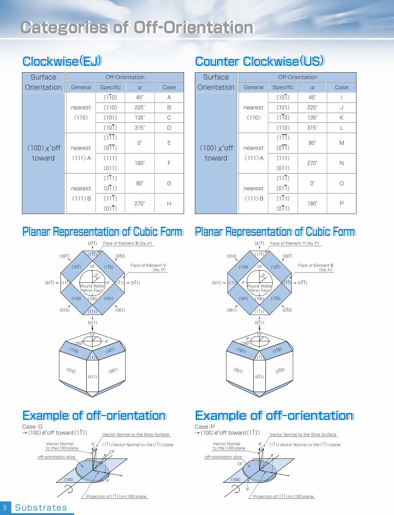
Categories of Off-OrientationCategories of Off-Orientation
Clockwise(EJ)
Example of off-orientation
Surface
Orientation
(100)χ°off
toward
Off-Orientation
General
nearest
〈110〉
nearest
〈111〉A
nearest
〈111〉B
Specific
〔110〕
〔110〕
〔101〕
〔101〕
〔111〕
〔011〕
〔111〕
〔011〕
〔111〕
〔011〕
〔111〕
〔011〕
α
45°
225°
135°
315°
0°
180°
90°
270°
Case
A
B
C
D
E
F
G
H
Counter Clockwise(US)Surface
Orientation
(100)χ°off
toward
Off-Orientation
General
nearest
〈110〉
nearest
〈111〉A
nearest
〈111〉B
Specific
〔101〕
〔101〕
〔110〕
〔110〕
〔111〕
〔011〕
〔111〕
〔011〕
〔111〕
〔011〕
〔111〕
〔011〕
α
45°
225°
135°
315°
90°
270°
0°
180°
Case
I
J
K
L
M
N
O
P
Vector Normal to the Slice Surface
Case:G →(100)θ°off toward〔111〕
Example of off-orientation
Clockwise(EJ)
Planar Representation of Cubic FormPlanar Representation of Cubic Form
Example of off-orientation
Planar Representation of Cubic FormPlanar Representation of Cubic Form
Counter Clockwise(US)
Example of off-orientationCase:P →(100)θ°off toward〔111〕
off-orientation slice
〔111〕Vector Normal to the(111)planeVector Normal to the(100)plane
Projection of〔111〕on(100)plane
OF
IF(100)
α
OF
OF
IF
IF
(110)
(111)
(111)
(101) (100)
(101) (110)
〔011〕 〔011〕
〔011〕
〔001〕
〔010〕 〔001〕
〔010〕
〔011〕
Face of Element Ⅲ(Ga, In)
Face of Element Ⅴ (As, P)
(111)
(011)
(010) (001)
(110) (101)
α
OF
OF
IF
IF
(101)
(111)
(111)
(111)
(111)
(110)
(110) (101)
〔011〕 〔011〕
〔011〕
〔010〕
〔001〕 〔010〕
〔001〕
〔011〕
Face of Element Ⅴ(As, P)
Face of Element Ⅲ (Ga, In)
(111)
(011)
(001) (010)
(101) (110)
(100)
(100)
(100)
(111) Round Wafer (Mirror Face)
Round Wafer (Mirror Face)
θ°
Vector Normal to the Slice Surface
off-orientation slice
〔111〕Vector Normal to the(111)planeVector Normal to the(100)plane
Projection of〔111〕on(100)plane
OF
IF
(100)
θ°
(111)