
EVALPWD5F60 - ST
10
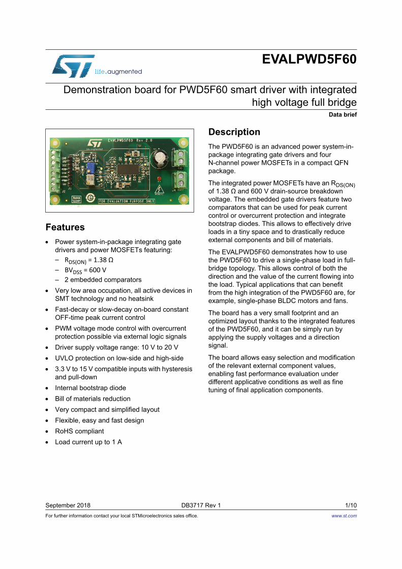
For further information contact your local STMicroelectronics sales office. September 2018 DB3717 Rev 1 1/10 EVALPWD5F60 Demonstration board for PWD5F60 smart driver with integrated high voltage full bridge Data brief Features Power system-in-package integrating gate drivers and power MOSFETs featuring: – R DS(ON) = 1.38 Ω – BV DSS = 600 V – 2 embedded comparators Very low area occupation, all active devices in SMT technology and no heatsink Fast-decay or slow-decay on-board constant OFF-time peak current control PWM voltage mode control with overcurrent protection possible via external logic signals Driver supply voltage range: 10 V to 20 V UVLO protection on low-side and high-side 3.3 V to 15 V compatible inputs with hysteresis and pull-down Internal bootstrap diode Bill of materials reduction Very compact and simplified layout Flexible, easy and fast design RoHS compliant Load current up to 1 A Description The PWD5F60 is an advanced power system-in- package integrating gate drivers and four N-channel power MOSFETs in a compact QFN package. The integrated power MOSFETs have an R DS(ON) of 1.38 Ω and 600 V drain-source breakdown voltage. The embedded gate drivers feature two comparators that can be used for peak current control or overcurrent protection and integrate bootstrap diodes. This allows to effectively drive loads in a tiny space and to drastically reduce external components and bill of materials. The EVALPWD5F60 demonstrates how to use the PWD5F60 to drive a single-phase load in full- bridge topology. This allows control of both the direction and the value of the current flowing into the load. Typical applications that can benefit from the high integration of the PWD5F60 are, for example, single-phase BLDC motors and fans. The board has a very small footprint and an optimized layout thanks to the integrated features of the PWD5F60, and it can be simply run by applying the supply voltages and a direction signal. The board allows easy selection and modification of the relevant external component values, enabling fast performance evaluation under different applicative conditions as well as fine tuning of final application components. www.st.com
Transcript of EVALPWD5F60 - ST
For further information contact your local STMicroelectronics sales office.
September 2018 DB3717 Rev 1 1/10
EVALPWD5F60
Demonstration board for PWD5F60 smart driver with integratedhigh voltage full bridge
Data brief
Features Power system-in-package integrating gate
drivers and power MOSFETs featuring:– RDS(ON) = 1.38 Ω– BVDSS = 600 V– 2 embedded comparators
Very low area occupation, all active devices in SMT technology and no heatsink
Fast-decay or slow-decay on-board constant OFF-time peak current control
PWM voltage mode control with overcurrent protection possible via external logic signals
Driver supply voltage range: 10 V to 20 V UVLO protection on low-side and high-side 3.3 V to 15 V compatible inputs with hysteresis
and pull-down Internal bootstrap diode Bill of materials reduction Very compact and simplified layout Flexible, easy and fast design RoHS compliant Load current up to 1 A
DescriptionThe PWD5F60 is an advanced power system-in-package integrating gate drivers and four N-channel power MOSFETs in a compact QFN package.
The integrated power MOSFETs have an RDS(ON) of 1.38 Ω and 600 V drain-source breakdown voltage. The embedded gate drivers feature two comparators that can be used for peak current control or overcurrent protection and integrate bootstrap diodes. This allows to effectively drive loads in a tiny space and to drastically reduce external components and bill of materials.
The EVALPWD5F60 demonstrates how to use the PWD5F60 to drive a single-phase load in full-bridge topology. This allows control of both the direction and the value of the current flowing into the load. Typical applications that can benefit from the high integration of the PWD5F60 are, for example, single-phase BLDC motors and fans.
The board has a very small footprint and an optimized layout thanks to the integrated features of the PWD5F60, and it can be simply run by applying the supply voltages and a direction signal.
The board allows easy selection and modification of the relevant external component values, enabling fast performance evaluation under different applicative conditions as well as fine tuning of final application components.
www.st.com
Board description EVALPWD5F60
2/10 DB3717 Rev 1
1 Board description
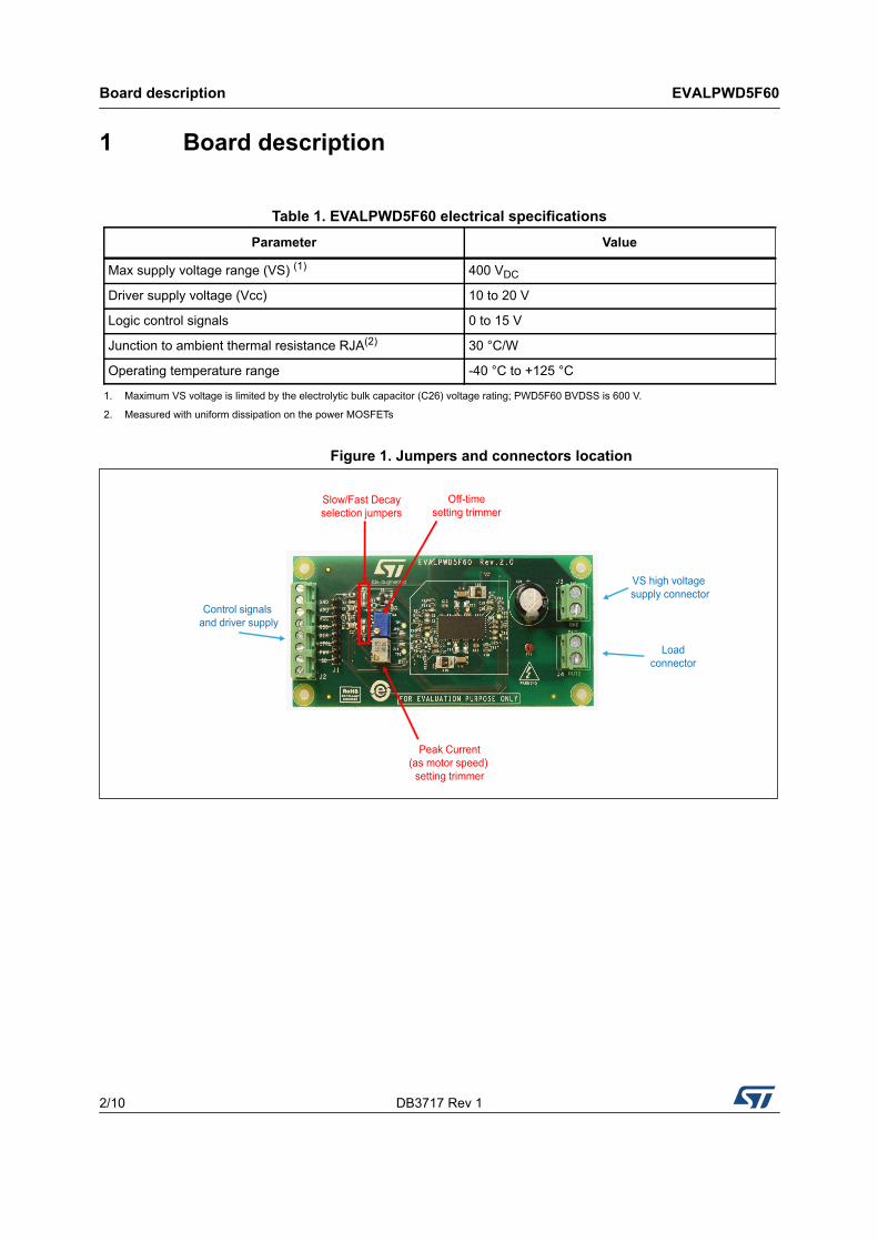
Figure 1. Jumpers and connectors location
Table 1. EVALPWD5F60 electrical specificationsParameter Value
Max supply voltage range (VS) (1) 400 VDC
Driver supply voltage (Vcc) 10 to 20 V
Logic control signals 0 to 15 V
Junction to ambient thermal resistance RJA(2) 30 °C/W
Operating temperature range -40 °C to +125 °C
1. Maximum VS voltage is limited by the electrolytic bulk capacitor (C26) voltage rating; PWD5F60 BVDSS is 600 V.
2. Measured with uniform dissipation on the power MOSFETs
Control signals and driver supply
VS high voltage supply connector
Loadconnector
Slow/Fast Decayselection jumpers
Peak Current(as motor speed)
setting trimmer
Off-timesetting trimmer
DB3717 Rev 1 3/10
EVALPWD5F60 Board description
10
Table 2. Jumpers and connectors descriptionName Type Function
J1 Control signals connector VCC and logic control signals, pin strip header
J2 Control signals connector VCC and logic control signals, terminal block connector
J3 Power supply VS high voltage power supply connector
J4 Power output Load connector
JP1 Configuration jumper To connect VPU pull-up voltage to VCC
JP2 Configuration jumper To pull-up SD or PWM signals to VPU pull-up voltage
JP3 Configuration jumper To connect SD or PWM signal to CPOUT2
JP4 Configuration jumper To use trimmer TR2 for setting the peak current instead ofR10
JP5 Configuration jumper To use trimmer TR1 for setting OFF-time duration afterovercurrent detection instead of R23
Table 3. Control signals connector pinout (J1 - J2)Pin Label Type Description
1 SD Digital input Drivers' SD signal
2 PWM Digital input Drivers' PWM signal
3 VCTRL Analog / PWM input Vctrl signal, sets current limit threshold (as motor speed)
4 DIR Digital input DIR signal, sets current's direction (as from Hall sensor)
5 RSD Reserved Reserved
6 VCC Power supply Drivers' VCC power supply
7 VPU Power supply VPU pull-up voltage for drivers' signals. Close JP1 to connect to VCC
8 GND Power supply GND
Schematic diagram EVALPWD5F60
4/10 DB3717 Rev 1
2 Schematic diagram
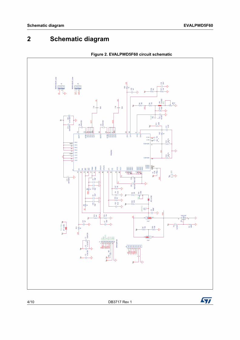
Figure 2. EVALPWD5F60 circuit schematicJ3
MORS
V-50
8-2P
_scr
ew
1 2
Vcc
Vpu
VS
RSD
Vctrl
SD PWM
DIR
J4
MORS
V-50
8-2P
_scr
ew
1 2
C21
1nF
OUT1
OUT2
U1
PWD5
F60
OUT1
EP5
OUT1
29OU
T127
OUT1
28OU
TB1
12
CPOU
T245
VS19
VS110
VS111
VS231
VS1EP3
SENSE23
GND1
16
GND1
22
GND1
26
PWM1
17
SD1
15
DT1
19
IN1
14
SENSE125
GND1
EP4
GND2
EP1
GND2
40GN
D24
CP+2
1
OUTB
234
OUT2
8OU
T27
OUT2
EP2
CPOU
T121
CP-2
2
CP+1
23
CP-1
24
VCC2
18
VCC1
42
OUT1
30
OUT2
6OU
T25
GND2
46
IN2
37
PWM2
41
SD2
38
DT2
43
VS232
VS233
VS2EP6
BOOT
113
BOOT
235
RSD136
RSD239
RSD3EP7
NC120
NC244
J1
STRI
P254
P-M-
8
1 2 3 4 5 6 7 8
DIR
C8 33pF
R18
1k
C9 33pF
R23
N.M.
N.M.
N.M.
Vpu
DIR_
N
C25
33pF
R5 1k
J21 2 3 4 5 6 7 8
VCC_
F
Vpu
RSD
Vctrl
SD PWM
DIR
R10
N.M.
C24
33pF
R6 1k
SD
PWM
TP1
R1 N.M.
Vpu
OUT1
RSD
Vctrl
RSD
TR2 1k
C7 33pF
TR1
C12
1uF/
25V
R8 30k
R4 30k
TR1
200k
Vs
R7 0R
C18
470n
F/25
V
R16
1R8
1%R1
51R
8 1%
R14
7.5k
R9 10k
R13
24k
C5 820p
F
VS1
TP5
TP3
C6
C11
3.3n
F
R12
1k
JP5
CLOS
E
C13
470n
F/25
V
C17
33nF
/630
V
Vpu
SD
C19
22nF
R17
3.9k
R19
24k
JP3
1 32
Vcc
JP2
1 32
R2 24k
Vpu
Vcc
INSD Vctr
l
GND
PWM
Vcc
Vcc-
Vpu
JP1
CLOS
EVp
u
JP4
CLOS
ED
TP4
GND
C26
4.7u
F/45
0VC1
433
nF/6
30V
C20
1nFR2
0
1K
DIR
PWM
VS1
C16
N.M.
OUT2
R11
220k
Vpu
Vpu
Vcc
Vpu
VSC1
5
N.M.
R21
0RC2
2
Vref
CPOU
T2
R22
10R
Vcc
Vpu
C3 4.7u
F/25
VC2 4.
7uF/
25V
VCC_
F
C1 100n
F/25
V
R3 220kC4
1uF/
25VVc
c
TR2
Q3
2N7002
2
1
3
C10
100n
F/25
V
TP2
R24
N.M.
Vcc
C23
100n
F/25
V
Vcc
SNS
DB3717 Rev 1 5/10
EVALPWD5F60 Schematic diagram
10
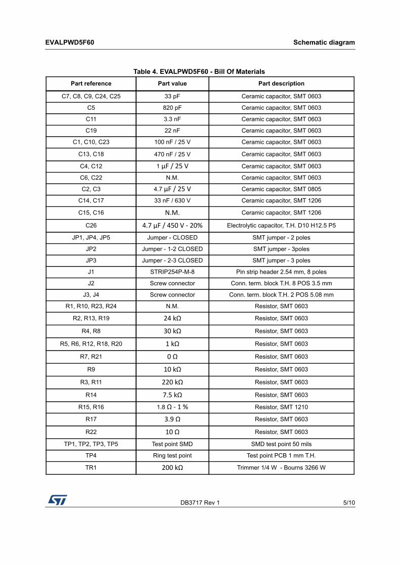
Table 4. EVALPWD5F60 - Bill Of Materials Part reference Part value Part description
C7, C8, C9, C24, C25 33 pF Ceramic capacitor, SMT 0603
C5 820 pF Ceramic capacitor, SMT 0603
C11 3.3 nF Ceramic capacitor, SMT 0603
C19 22 nF Ceramic capacitor, SMT 0603
C1, C10, C23 100 nF / 25 V Ceramic capacitor, SMT 0603
C13, C18 470 nF / 25 V Ceramic capacitor, SMT 0603
C4, C12 1 μF / 25 V Ceramic capacitor, SMT 0603
C6, C22 N.M. Ceramic capacitor, SMT 0603
C2, C3 4.7 μF / 25 V Ceramic capacitor, SMT 0805
C14, C17 33 nF / 630 V Ceramic capacitor, SMT 1206
C15, C16 N.M. Ceramic capacitor, SMT 1206
C26 4.7 μF / 450 V - 20% Electrolytic capacitor, T.H. D10 H12.5 P5
JP1, JP4, JP5 Jumper - CLOSED SMT jumper - 2 poles
JP2 Jumper - 1-2 CLOSED SMT jumper - 3poles
JP3 Jumper - 2-3 CLOSED SMT jumper - 3 poles
J1 STRIP254P-M-8 Pin strip header 2.54 mm, 8 poles
J2 Screw connector Conn. term. block T.H. 8 POS 3.5 mm
J3, J4 Screw connector Conn. term. block T.H. 2 POS 5.08 mm
R1, R10, R23, R24 N.M. Resistor, SMT 0603
R2, R13, R19 24 kΩ Resistor, SMT 0603
R4, R8 30 kΩ Resistor, SMT 0603
R5, R6, R12, R18, R20 1 kΩ Resistor, SMT 0603
R7, R21 0 Ω Resistor, SMT 0603
R9 10 kΩ Resistor, SMT 0603
R3, R11 220 kΩ Resistor, SMT 0603
R14 7.5 kΩ Resistor, SMT 0603
R15, R16 1.8 Ω - 1 % Resistor, SMT 1210
R17 3.9 Ω Resistor, SMT 0603
R22 10 Ω Resistor, SMT 0603
TP1, TP2, TP3, TP5 Test point SMD SMD test point 50 mils
TP4 Ring test point Test point PCB 1 mm T.H.
TR1 200 kΩ Trimmer 1/4 W - Bourns 3266 W
Schematic diagram EVALPWD5F60
6/10 DB3717 Rev 1
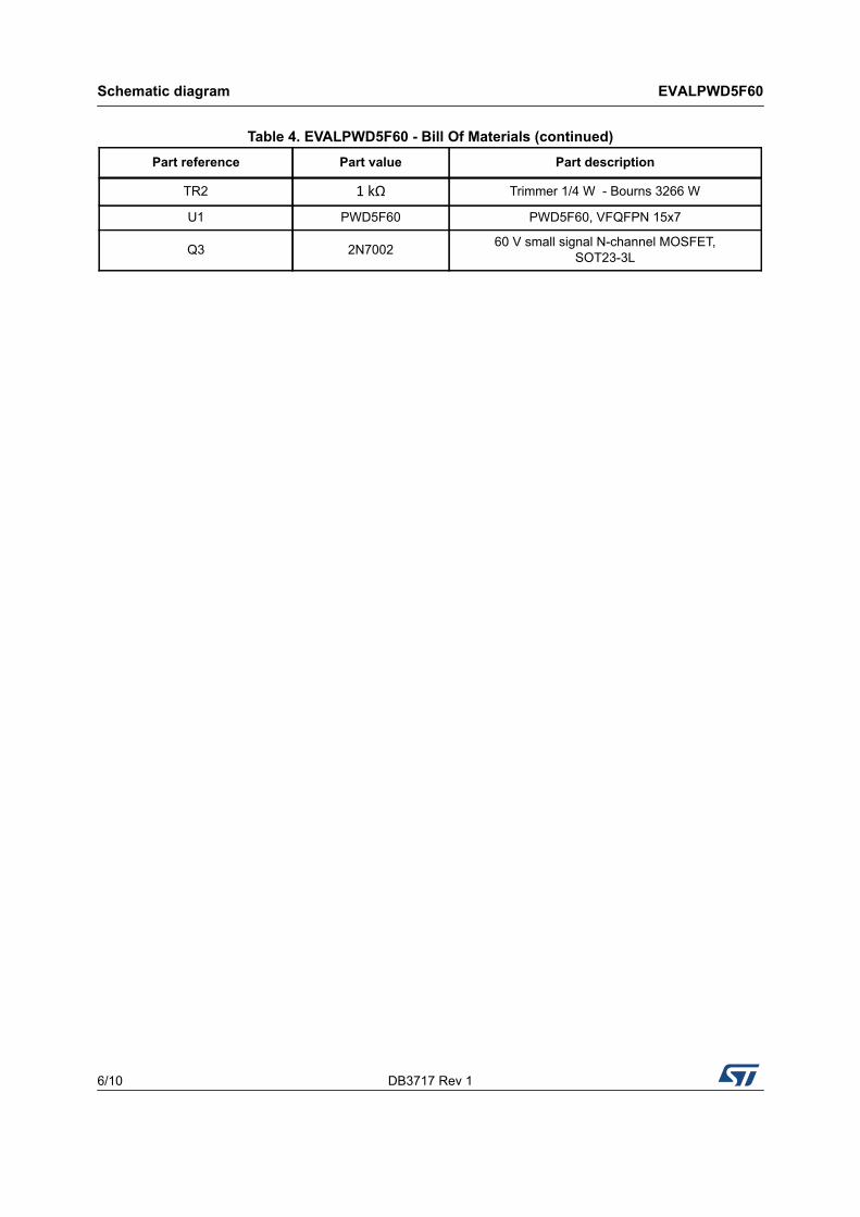
TR2 1 kΩ Trimmer 1/4 W - Bourns 3266 W
U1 PWD5F60 PWD5F60, VFQFPN 15x7
Q3 2N7002 60 V small signal N-channel MOSFET, SOT23-3L
Table 4. EVALPWD5F60 - Bill Of Materials (continued)Part reference Part value Part description
DB3717 Rev 1 7/10
EVALPWD5F60 Schematic diagram
10
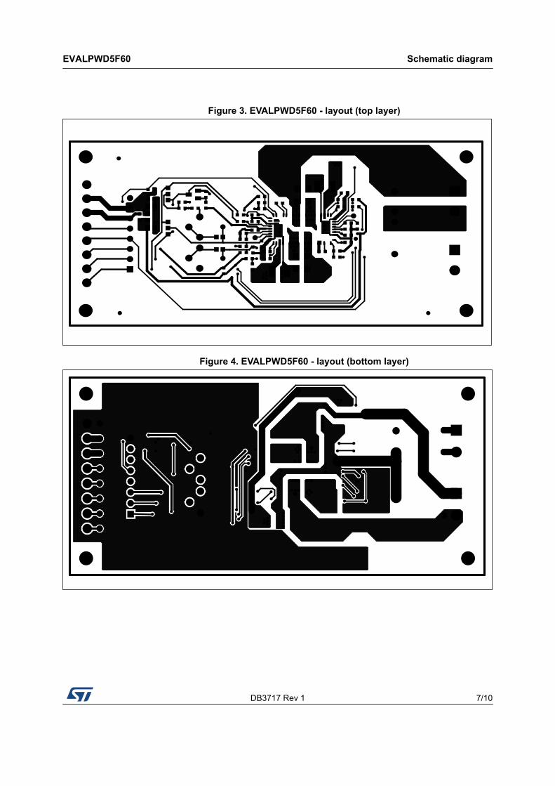
Figure 3. EVALPWD5F60 - layout (top layer)
Figure 4. EVALPWD5F60 - layout (bottom layer)
Schematic diagram EVALPWD5F60
8/10 DB3717 Rev 1
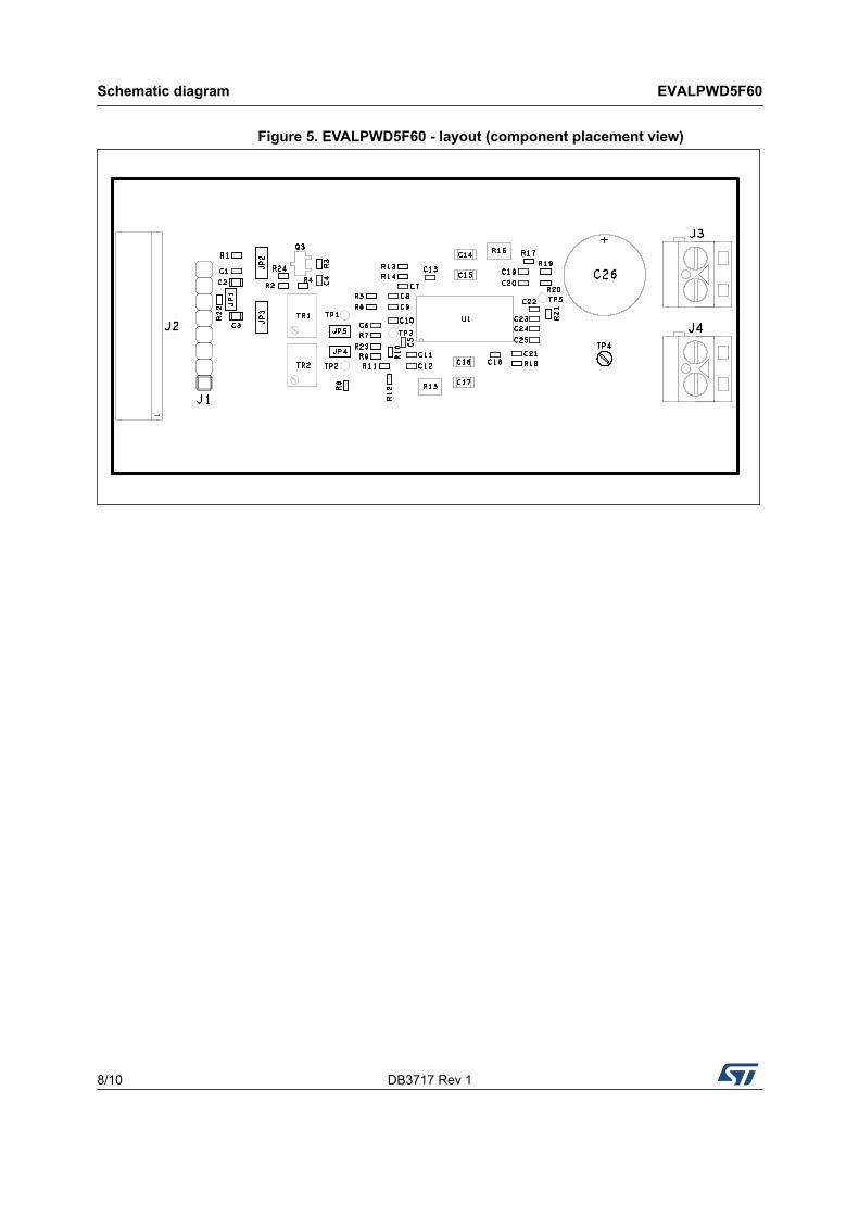
Figure 5. EVALPWD5F60 - layout (component placement view)
DB3717 Rev 1 9/10
EVALPWD5F60 Revision history
10
3 Revision history
Table 5. Document revision historyDate Revision Changes
29-Aug-2018 1 Initial release

EVALPWD5F60
10/10 DB3717 Rev 1
IMPORTANT NOTICE – PLEASE READ CAREFULLY
STMicroelectronics NV and its subsidiaries (“ST”) reserve the right to make changes, corrections, enhancements, modifications, and improvements to ST products and/or to this document at any time without notice. Purchasers should obtain the latest relevant information on ST products before placing orders. ST products are sold pursuant to ST’s terms and conditions of sale in place at the time of order acknowledgement.
Purchasers are solely responsible for the choice, selection, and use of ST products and ST assumes no liability for application assistance or the design of Purchasers’ products.
No license, express or implied, to any intellectual property right is granted by ST herein.
Resale of ST products with provisions different from the information set forth herein shall void any warranty granted by ST for such product.
ST and the ST logo are trademarks of ST. All other product or service names are the property of their respective owners.
Information in this document supersedes and replaces information previously supplied in any prior versions of this document.
© 2018 STMicroelectronics – All rights reserved