HICUM L0 1.2 experience on various ST BiCMOS technologies ...
27
21 th AKB (Bipolar ArbeitsKreis) HAMBURG – 2008 October 30th HICUM L0 1.2 experience on various ST BiCMOS technologies Nicolas DERRIER – STMicroelectronics Internal ref. : dm08.181
Transcript of HICUM L0 1.2 experience on various ST BiCMOS technologies ...
21th AKB (Bipolar ArbeitsKreis)HAMBURG – 2008 October 30th
HICUM L0 1.2 experience on various ST BiCMOS technologies Nicolas DERRIER – STMicroelectronics
Internal ref. : dm08.181
2AKB 2008 Hamburg – N. Derrier HICUM L0 1.2 experience on various ST BiCMOS technologies
OUTLINE
• Motivation
• About the parameters translation
• HICUM L0 1.2 results for the ST 0.25μm SiGe-C technology
• HICUM L0 1.2 results for the ST 0.13μm SiGe-C “low-cost” technology
• HICUM L0 1.2 results for the ST 0.13μm SiGe-C MMW technology
• Conclusion
• References
3AKB 2008 Hamburg – N. Derrier HICUM L0 1.2 experience on various ST BiCMOS technologies
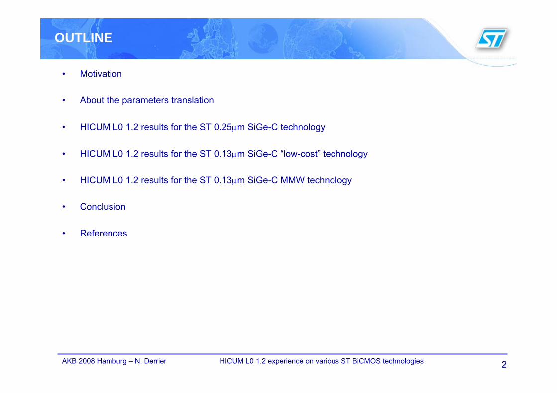
MOTIVATION (1/3)
• Last HICUM WS 2008 Böblingen :“From HICUM level 2 to HICUM level 0”, N. Derrier, STMicroelectronics [3]Presentation of a complete set of equations to translate directly HICUM L2 parameters into HICUM L0 ones.
• Yes, but some HICUM L0 known issues, especially the collector current @high current density, fTinstability, unaccuracy of temperature behavior (mCF) ([2],[3],[4],[6],[7])
• The direct translation of some parameters does not work, like IQFH, TFH etc… :
IC @VBC=0V
0
0
*
2
=
=
HQ F H
F
C S
E F
H CH
P
S
I
T
Qτ
ττ
IB=0.8μA
IB=8μA
IB=17μA (≈fT peak)
IB=41μA
4AKB 2008 Hamburg – N. Derrier HICUM L0 1.2 experience on various ST BiCMOS technologies
MOTIVATION (2/3)
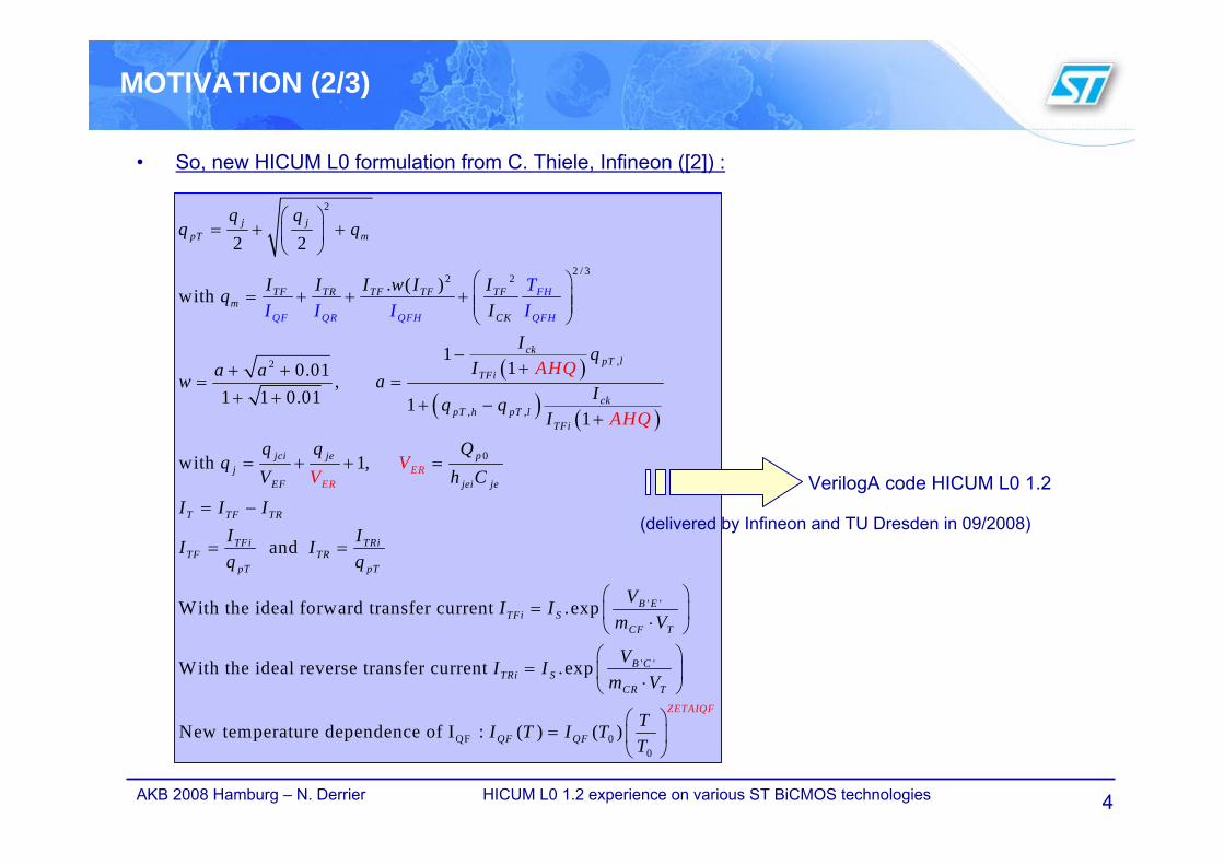
• So, new HICUM L0 formulation from C. Thiele, Infineon ([2]) :
( )
( ) ( )
2
2 / 32 2
,2
, ,
0
2 2
. ( )with
110.01 ,
1 1 0.01 11
with 1,
⎛ ⎞= + +⎜ ⎟
⎝ ⎠
⎛ ⎞= + + + ⎜ ⎟⎜ ⎟
⎝ ⎠
−++ +
= =+ + + −
+
= + + =
j jpT m
TF TR TF TF TFm
CK
ckpT l
TFi
ckpT h pT
FH
QF Q
lTFi
jci je pj
EFER
E
R QFH Q H
j
F
eR i j
TI I I I
q qq q
I I I w I IqI
I qIa aw a Iq q
I
A
q q Qq
V
HQ
Vh
A Q
V C
H
' '
' '
and
With the ideal forward transfer current .exp
With the ideal reverse transfer current .exp
New temperature dependen
= −
= =
⎛ ⎞= ⎜ ⎟⋅⎝ ⎠
⎛ ⎞= ⎜ ⎟⋅⎝ ⎠
e
T TF TR
TFi TRiTF TR
pT pT
B ETFi S
CF T
B CTRi S
CR T
I I II II Iq q
VI Im V
VI Im V
QF 00
ce of I : ( ) ( )⎛ ⎞
= ⎜ ⎟⎝ ⎠
QF QF
ZETAIQFTI T I TT
VerilogA code HICUM L0 1.2
(delivered by Infineon and TU Dresden in 09/2008)
5AKB 2008 Hamburg – N. Derrier HICUM L0 1.2 experience on various ST BiCMOS technologies
MOTIVATION (3/3)
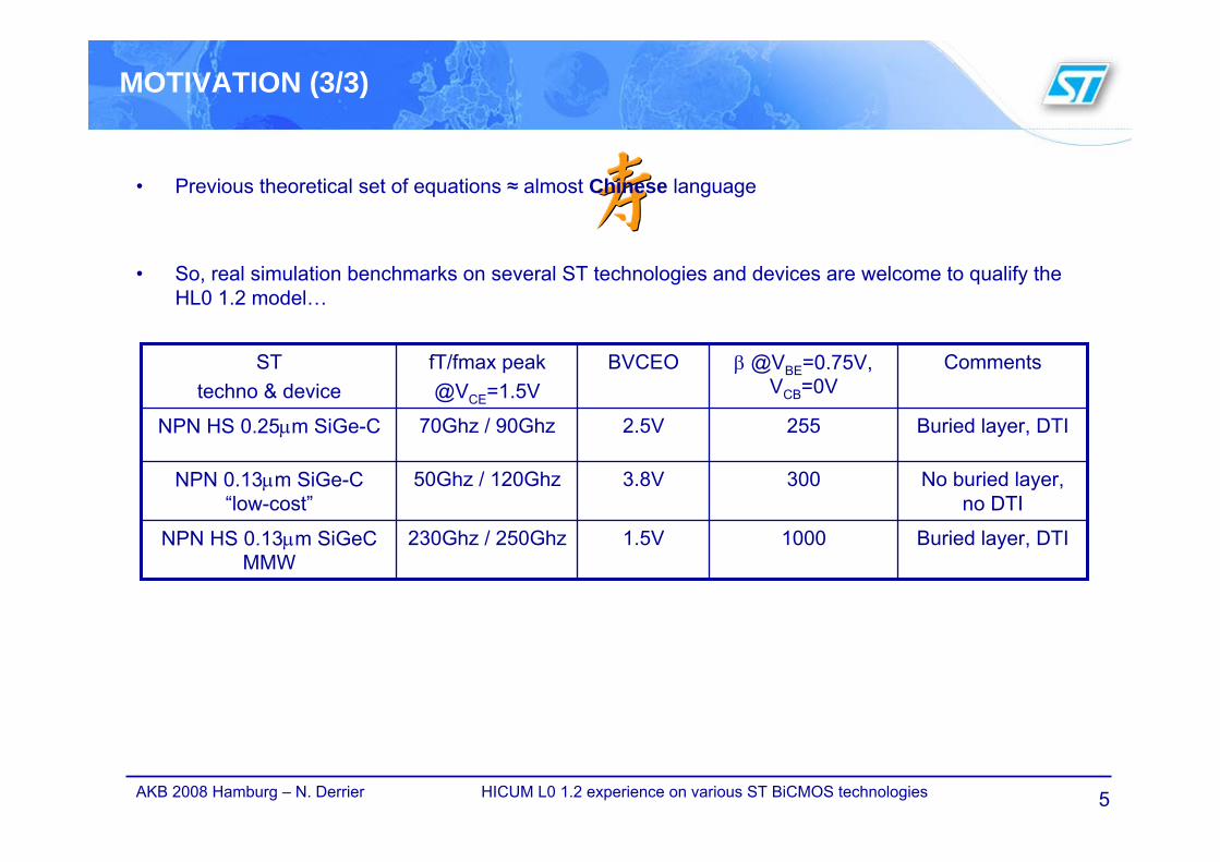
• Previous theoretical set of equations ≈ almost Chinese language
• So, real simulation benchmarks on several ST technologies and devices are welcome to qualify the HL0 1.2 model…
Buried layer, DTI10001.5V230Ghz / 250GhzNPN HS 0.13μm SiGeCMMW
No buried layer, no DTI
3003.8V50Ghz / 120GhzNPN 0.13μm SiGe-C “low-cost”
Buried layer, DTI2552.5V70Ghz / 90GhzNPN HS 0.25μm SiGe-C
Commentsβ @VBE=0.75V, VCB=0V
BVCEOfT/fmax peak@VCE=1.5V
ST techno & device
6AKB 2008 Hamburg – N. Derrier HICUM L0 1.2 experience on various ST BiCMOS technologies
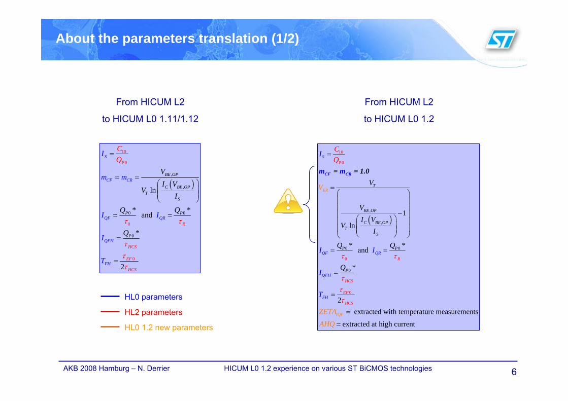
About the parameters translation (1/2)
( )
10
0
0
0
,
,
0 0
0
ln
* * and
*
2
=
= =⎛ ⎞⎜ ⎟⎜ ⎟⎝ ⎠
= =
=
=
P
R
HCS
E
S
C
F
H
BE OP
C BE OPT
S
P P
CS
F CR
QF QR
FH
PQFH
VI V
VI
Q Q
I
m m
I I
Q
CQ
I
T
τ τ
τττ
From HICUM L2
to HICUM L0 1.11/1.12
From HICUM L2
to HICUM L0 1.2
( ),
,
10
0
0
0
0 0
0
1
ln
* * and
*
2extracted with temperature measurements
extracted at high current
=
=⎛ ⎞⎜ ⎟⎜ ⎟
−⎜ ⎟⎛ ⎞⎜ ⎟⎜ ⎟⎜ ⎟⎜ ⎟⎝ ⎠⎝ ⎠
= =
=
=
=
=
S
QF QR
QFH
T
BE OP
C BE OPT
S
P P
P
ER
I
P
R
HCS
EF
HCSFH
QF
V
Z
I
I
V
VI V
VI
Q I
I
T
ETA
A
C
Q
Q
H
Q
Qτ τ
τττ
CF CR= = 1.m m 0
HL0 parameters
HL0 1.2 new parameters
HL2 parameters
7AKB 2008 Hamburg – N. Derrier HICUM L0 1.2 experience on various ST BiCMOS technologies
About the parameters translation (2/2)
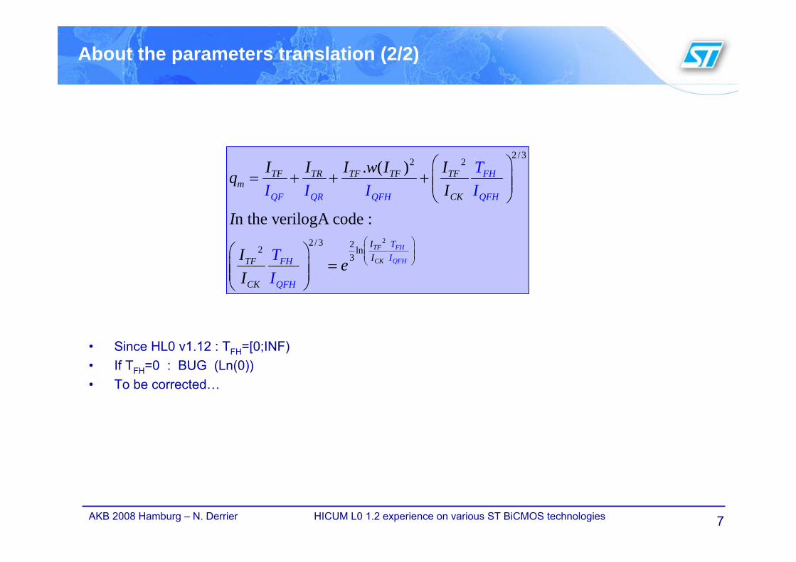
2
2 /32 2
2/3 22 ln3
. ( )
n the verilogA code :⎛ ⎞⎜ ⎟⎜ ⎟⎝ ⎠
⎛ ⎞= + + + ⎜ ⎟⎜ ⎟
⎝ ⎠
⎛ ⎞=⎜ ⎟⎜ ⎟
⎝ ⎠
FTF
C QK
H
FH
TF TR TF TF TFm
CK
IITF
C
FH
QF QR QFH QFH
TIH
QFK
F
H
TI II I I w I Iq
I
I
I e
I I
TI I
• Since HL0 v1.12 : TFH=[0;INF)• If TFH=0 : BUG (Ln(0))• To be corrected…
8AKB 2008 Hamburg – N. Derrier HICUM L0 1.2 experience on various ST BiCMOS technologies
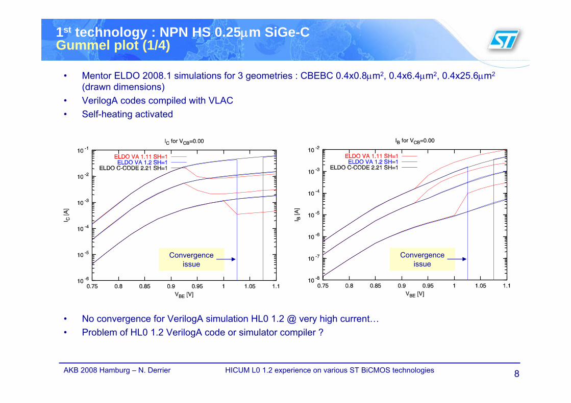
1st technology : NPN HS 0.25μm SiGe-CGummel plot (1/4)
• Mentor ELDO 2008.1 simulations for 3 geometries : CBEBC 0.4x0.8μm2, 0.4x6.4μm2, 0.4x25.6μm2
(drawn dimensions)• VerilogA codes compiled with VLAC• Self-heating activated
• No convergence for VerilogA simulation HL0 1.2 @ very high current…• Problem of HL0 1.2 VerilogA code or simulator compiler ?
Convergence issue
Convergence issue
9AKB 2008 Hamburg – N. Derrier HICUM L0 1.2 experience on various ST BiCMOS technologies
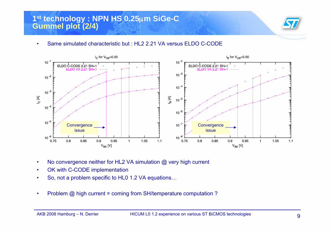
1st technology : NPN HS 0.25μm SiGe-CGummel plot (2/4)
• Same simulated characteristic but : HL2 2.21 VA versus ELDO C-CODE
• No convergence neither for HL2 VA simulation @ very high current• OK with C-CODE implementation• So, not a problem specific to HL0 1.2 VA equations…
• Problem @ high current = coming from SH/temperature computation ?
Convergence issue
Convergence issue
10AKB 2008 Hamburg – N. Derrier HICUM L0 1.2 experience on various ST BiCMOS technologies
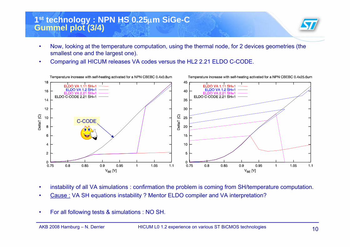
1st technology : NPN HS 0.25μm SiGe-CGummel plot (3/4)
• Now, looking at the temperature computation, using the thermal node, for 2 devices geometries (the smallest one and the largest one).
• Comparing all HICUM releases VA codes versus the HL2 2.21 ELDO C-CODE.
• instability of all VA simulations : confirmation the problem is coming from SH/temperature computation.• Cause : VA SH equations instability ? Mentor ELDO compiler and VA interpretation?
• For all following tests & simulations : NO SH.
C-CODE
11AKB 2008 Hamburg – N. Derrier HICUM L0 1.2 experience on various ST BiCMOS technologies
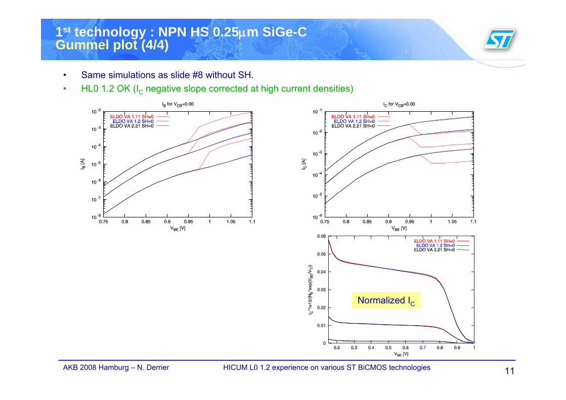
1st technology : NPN HS 0.25μm SiGe-CGummel plot (4/4)
• Same simulations as slide #8 without SH.• HL0 1.2 OK (IC negative slope corrected at high current densities)
Normalized IC
12AKB 2008 Hamburg – N. Derrier HICUM L0 1.2 experience on various ST BiCMOS technologies
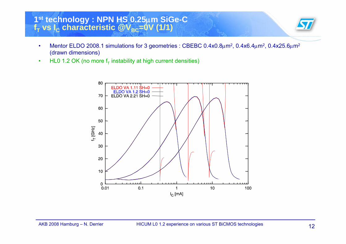
1st technology : NPN HS 0.25μm SiGe-CfT vs IC characteristic @VBC=0V (1/1)
• Mentor ELDO 2008.1 simulations for 3 geometries : CBEBC 0.4x0.8μm2, 0.4x6.4μm2, 0.4x25.6μm2
(drawn dimensions)• HL0 1.2 OK (no more fT instability at high current densities)
13AKB 2008 Hamburg – N. Derrier HICUM L0 1.2 experience on various ST BiCMOS technologies
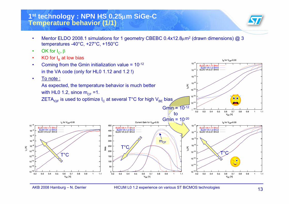
1st technology : NPN HS 0.25μm SiGe-CTemperature behavior (1/1)
• Mentor ELDO 2008.1 simulations for 1 geometry CBEBC 0.4x12.8μm2 (drawn dimensions) @ 3 temperatures -40°C, +27°C, +150°C
• OK for IC, β• KO for IB at low bias• Coming from the Gmin initialization value = 10-12
in the VA code (only for HL0 1.12 and 1.2 !)• To note :
As expected, the temperature behavior is much better with HL0 1.2, since mCF =1.ZETAIQF is used to optimize IC at several T°C for high VBE bias
T°CT°C
T°C
mCF
Gmin = 10-12
toGmin = 10-20
14AKB 2008 Hamburg – N. Derrier HICUM L0 1.2 experience on various ST BiCMOS technologies
IQFH,TFH to be optimized here…
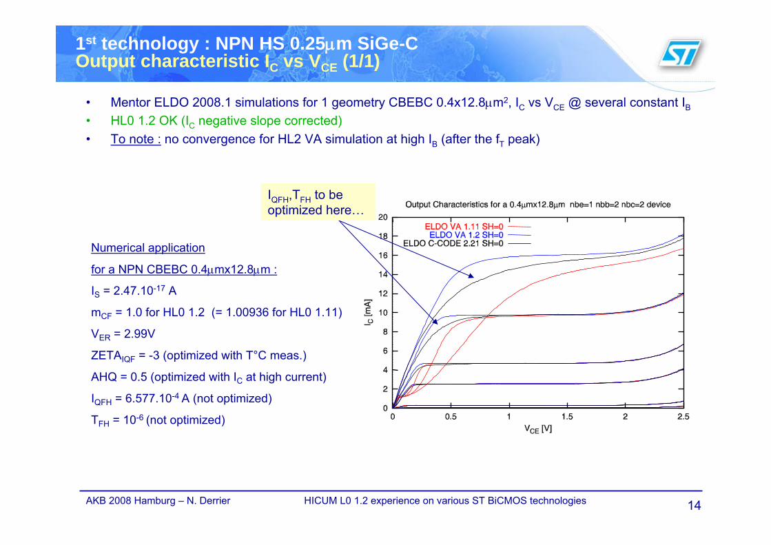
1st technology : NPN HS 0.25μm SiGe-COutput characteristic IC vs VCE (1/1)
• Mentor ELDO 2008.1 simulations for 1 geometry CBEBC 0.4x12.8μm2, IC vs VCE @ several constant IB• HL0 1.2 OK (IC negative slope corrected)• To note : no convergence for HL2 VA simulation at high IB (after the fT peak)
Numerical application
for a NPN CBEBC 0.4μmx12.8μm :
IS = 2.47.10-17 A
mCF = 1.0 for HL0 1.2 (= 1.00936 for HL0 1.11)
VER = 2.99V
ZETAIQF = -3 (optimized with T°C meas.)
AHQ = 0.5 (optimized with IC at high current)
IQFH = 6.577.10-4 A (not optimized)
TFH = 10-6 (not optimized)
15AKB 2008 Hamburg – N. Derrier HICUM L0 1.2 experience on various ST BiCMOS technologies
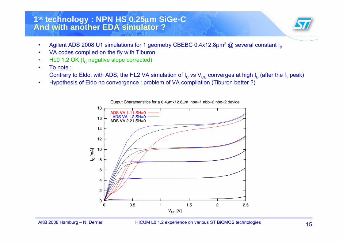
1st technology : NPN HS 0.25μm SiGe-CAnd with another EDA simulator ?
• Agilent ADS 2008.U1 simulations for 1 geometry CBEBC 0.4x12.8μm2 @ several constant IB• VA codes compiled on the fly with Tiburon• HL0 1.2 OK (IC negative slope corrected)• To note :
Contrary to Eldo, with ADS, the HL2 VA simulation of IC vs VCE converges at high IB (after the fT peak)• Hypothesis of Eldo no convergence : problem of VA compilation (Tiburon better ?)
16AKB 2008 Hamburg – N. Derrier HICUM L0 1.2 experience on various ST BiCMOS technologies
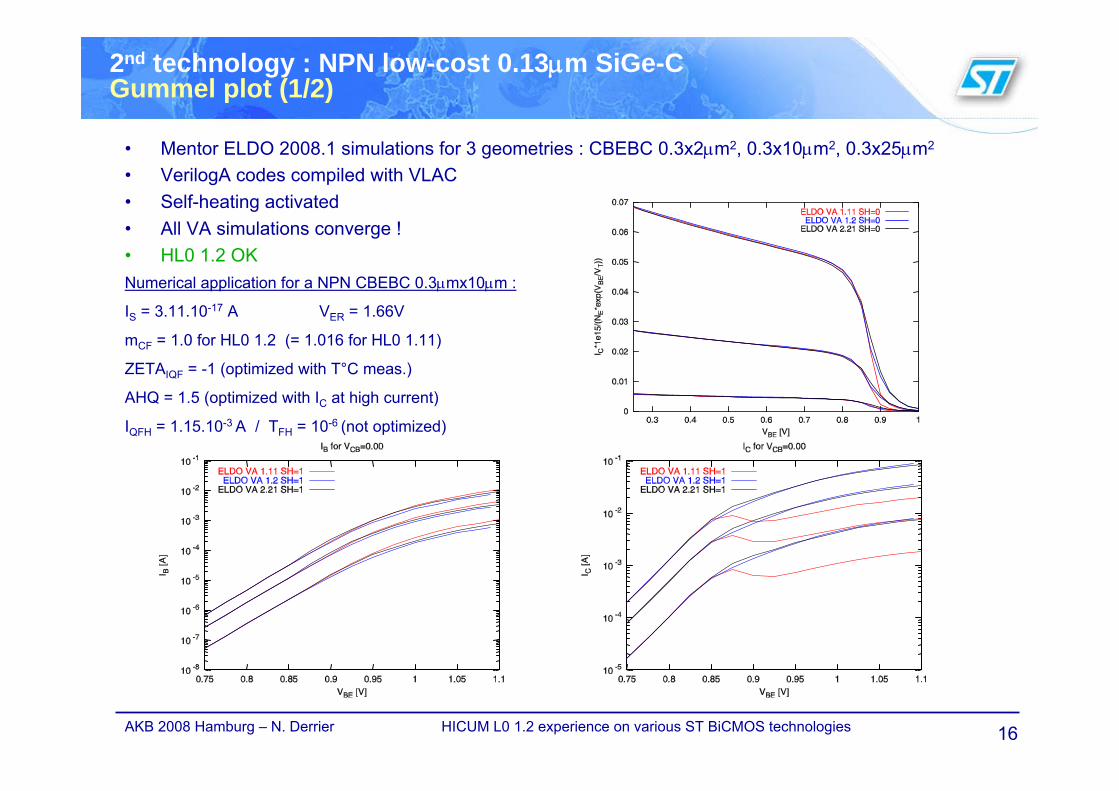
2nd technology : NPN low-cost 0.13μm SiGe-CGummel plot (1/2)
• Mentor ELDO 2008.1 simulations for 3 geometries : CBEBC 0.3x2μm2, 0.3x10μm2, 0.3x25μm2
• VerilogA codes compiled with VLAC• Self-heating activated• All VA simulations converge !• HL0 1.2 OKNumerical application for a NPN CBEBC 0.3μmx10μm :
IS = 3.11.10-17 A VER = 1.66V
mCF = 1.0 for HL0 1.2 (= 1.016 for HL0 1.11)
ZETAIQF = -1 (optimized with T°C meas.)
AHQ = 1.5 (optimized with IC at high current)
IQFH = 1.15.10-3 A / TFH = 10-6 (not optimized)
17AKB 2008 Hamburg – N. Derrier HICUM L0 1.2 experience on various ST BiCMOS technologies
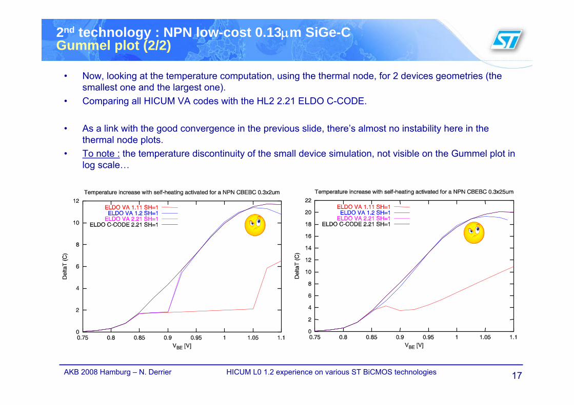
2nd technology : NPN low-cost 0.13μm SiGe-CGummel plot (2/2)
• Now, looking at the temperature computation, using the thermal node, for 2 devices geometries (the smallest one and the largest one).
• Comparing all HICUM VA codes with the HL2 2.21 ELDO C-CODE.
• As a link with the good convergence in the previous slide, there’s almost no instability here in the thermal node plots.
• To note : the temperature discontinuity of the small device simulation, not visible on the Gummel plot in log scale…
18AKB 2008 Hamburg – N. Derrier HICUM L0 1.2 experience on various ST BiCMOS technologies
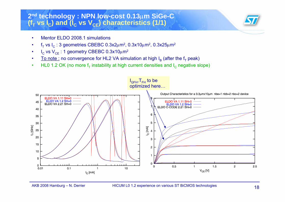
2nd technology : NPN low-cost 0.13μm SiGe-C (fT vs IC) and (IC vs VCE) characteristics (1/1)
• Mentor ELDO 2008.1 simulations • fT vs IC : 3 geometries CBEBC 0.3x2μm2, 0.3x10μm2, 0.3x25μm2
• IC vs VCE : 1 geometry CBEBC 0.3x10μm2
• To note : no convergence for HL2 VA simulation at high IB (after the fT peak)• HL0 1.2 OK (no more fT instability at high current densities and IC negative slope)
IQFH,TFH to be optimized here…
19AKB 2008 Hamburg – N. Derrier HICUM L0 1.2 experience on various ST BiCMOS technologies
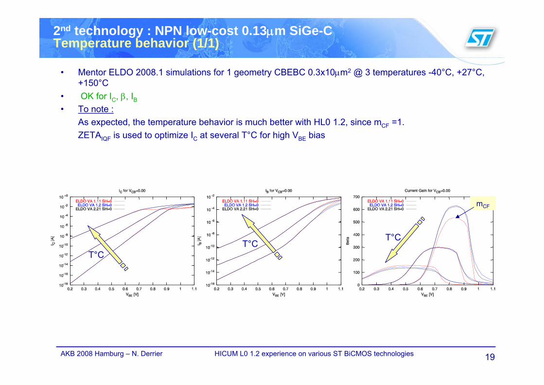
2nd technology : NPN low-cost 0.13μm SiGe-C Temperature behavior (1/1)
• Mentor ELDO 2008.1 simulations for 1 geometry CBEBC 0.3x10μm2 @ 3 temperatures -40°C, +27°C, +150°C
• OK for IC, β, IB• To note :
As expected, the temperature behavior is much better with HL0 1.2, since mCF =1.ZETAIQF is used to optimize IC at several T°C for high VBE bias
T°CT°C
T°C
mCF
20AKB 2008 Hamburg – N. Derrier HICUM L0 1.2 experience on various ST BiCMOS technologies
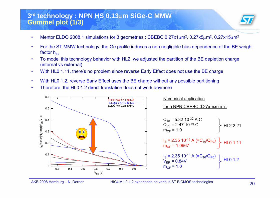
3rd technology : NPN HS 0.13μm SiGe-C MMW Gummel plot (1/3)
• Mentor ELDO 2008.1 simulations for 3 geometries : CBEBC 0.27x1μm2, 0.27x5μm2, 0.27x15μm2
• For the ST MMW technology, the Ge profile induces a non negligible bias dependence of the BE weight factor hjEi
• To model this technology behavior with HL2, we adjusted the partition of the BE depletion charge (internal vs external)
• With HL0 1.11, there’s no problem since reverse Early Effect does not use the BE charge
• With HL0 1.2, reverse Early Effect uses the BE charge without any possible partitioning• Therefore, the HL0 1.2 direct translation does not work anymore
Numerical application
for a NPN CBEBC 0.27μmx5μm :
C10 = 5.82 10-32 A.CQP0 = 2.47 10-16 CmCF = 1.0
IS = 2.35 10-16 A (=C10/QP0)mCF = 1.0967
IS = 2.35 10-16 A (=C10/QP0)VER = 0.84VmCF = 1.0
HL0 1.11
HL0 1.2
HL2 2.21
21AKB 2008 Hamburg – N. Derrier HICUM L0 1.2 experience on various ST BiCMOS technologies
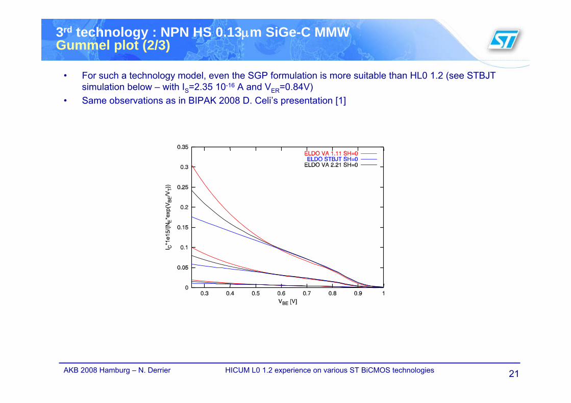
3rd technology : NPN HS 0.13μm SiGe-C MMW Gummel plot (2/3)
• For such a technology model, even the SGP formulation is more suitable than HL0 1.2 (see STBJT simulation below – with IS=2.35 10-16 A and VER=0.84V)
• Same observations as in BIPAK 2008 D. Celi’s presentation [1]
22AKB 2008 Hamburg – N. Derrier HICUM L0 1.2 experience on various ST BiCMOS technologies
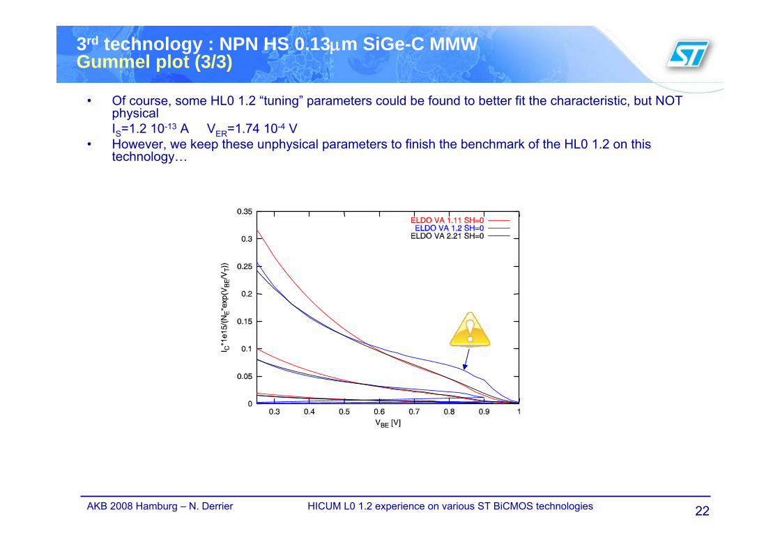
3rd technology : NPN HS 0.13μm SiGe-C MMW Gummel plot (3/3)
• Of course, some HL0 1.2 “tuning” parameters could be found to better fit the characteristic, but NOT physicalIS=1.2 10-13 A VER=1.74 10-4 V
• However, we keep these unphysical parameters to finish the benchmark of the HL0 1.2 on this technology…
23AKB 2008 Hamburg – N. Derrier HICUM L0 1.2 experience on various ST BiCMOS technologies
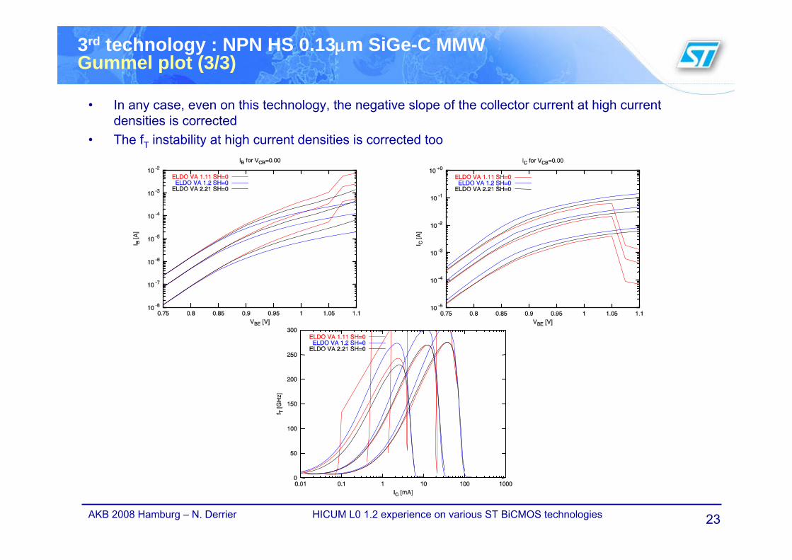
3rd technology : NPN HS 0.13μm SiGe-C MMW Gummel plot (3/3)
• In any case, even on this technology, the negative slope of the collector current at high current densities is corrected
• The fT instability at high current densities is corrected too
24AKB 2008 Hamburg – N. Derrier HICUM L0 1.2 experience on various ST BiCMOS technologies
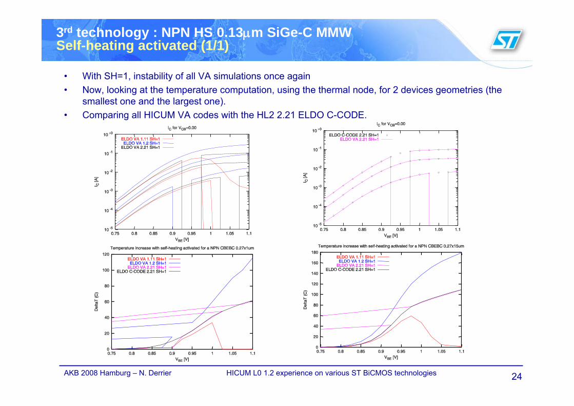
3rd technology : NPN HS 0.13μm SiGe-C MMW Self-heating activated (1/1)
• With SH=1, instability of all VA simulations once again• Now, looking at the temperature computation, using the thermal node, for 2 devices geometries (the
smallest one and the largest one).• Comparing all HICUM VA codes with the HL2 2.21 ELDO C-CODE.
25AKB 2008 Hamburg – N. Derrier HICUM L0 1.2 experience on various ST BiCMOS technologies
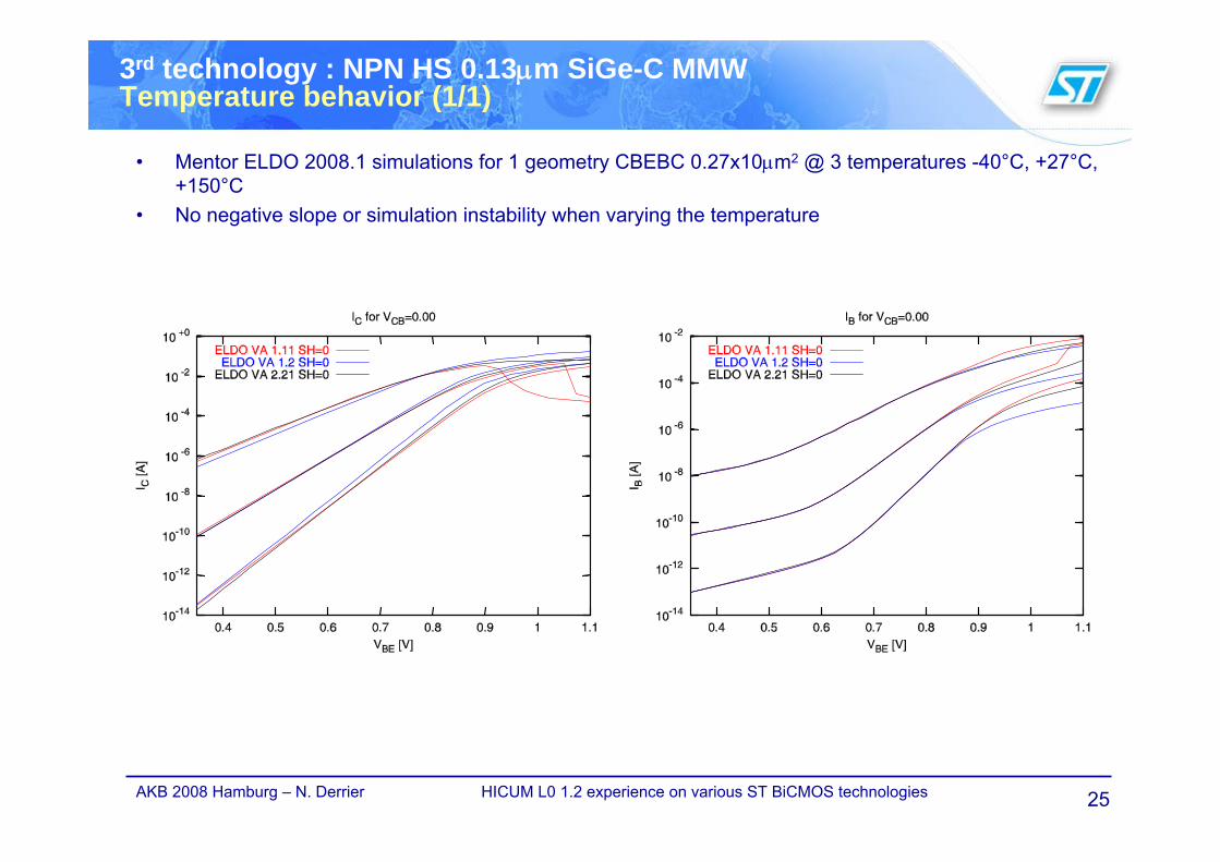
3rd technology : NPN HS 0.13μm SiGe-C MMW Temperature behavior (1/1)
• Mentor ELDO 2008.1 simulations for 1 geometry CBEBC 0.27x10μm2 @ 3 temperatures -40°C, +27°C, +150°C
• No negative slope or simulation instability when varying the temperature
26AKB 2008 Hamburg – N. Derrier HICUM L0 1.2 experience on various ST BiCMOS technologies
CONCLUSION
• A practical validation of the new release v1.2 of HICUM L0 has been done using 3 representative ST BiCMOS technologies.
• We compared different HICUM releases (L0 1.2, L0 1.11, L2 2.21), using VA codes and internal C-codes, mainly with Mentor ELDO (with Agilent ADS too for some characteristics).
• We extracted/optimized the HL0 v1.2 parameters (TFH, IQFH, AHQ, ZETAIQF) with success.
• HICUM L0 1.2 shows very good results, whatever the technology and the device geometry, and it eliminates the known issues of releases 1.11/1.12 :– No more negative slope of the collector current in
27AKB 2008 Hamburg – N. Derrier HICUM L0 1.2 experience on various ST BiCMOS technologies
REFERENCE
[1] D. Celi, “HICUM L0 v1.2 Parameter Extraction and Validation”, 21th Working Group Bipolar (BIPAK), Hamburg, October 2008
[2] C. Thiele, “A new explicit expression for the normalized hole charge improves the accuracy of HICUM/L0”, BCTM October 2008, Monterey
[3] N. Derrier, “From HICUM L2 to HICUM L0”, 8th HICUM workshop, Böblingen, May 2008[4] C. Thiele, “Further Developments of the HICUM L0 model”, 8th HICUM workshop, Böblingen, May
2008
[5] M. Schröter, S. Lehmann, A. Mukherjee, “HICUM/L0: A Simplified Compact Bipolar Transistor Model”, Manual Version 1.12, 2007
[6] H. Beckrich-Ros, F. Pourchon, “HICUM Level 0 Temperature Modeling: Towards Improvement”, 7th European HICUM Workshop, Dresden, June 2007
[7] C. Thiele, “HICUM/L0: Investigation and Improvement of the DC-High Current Modeling”, 7th European HICUM Workshop, Dresden, June 2007
[8] M. Schröter et al., “A Computationally Efficient Physics-Based Compact Bipolar Transistor Model for Circuit Design – Part I: Model Formulation”, IEEE Trans. on Elec. Dev., Vol. 53, no 2, February 2006
[9] D. Céli, “About Modeling the Reverse Early Effect in HICUM/Level 0”, 6th European HICUM Workshop, Heilbronn, June 2006


![A Wideband 77GHz, 17.5dBm Power Amplifier in Siliconhajimiri/pdf/77GHz PA-Komijani.pdf · SiGe BiCMOS process. ... and automotive radar (e.g., 77GHz band) [1][2][3]. ... approximately](https://static.fdocument.org/doc/165x107/5b57e9367f8b9a657c8b4e29/a-wideband-77ghz-175dbm-power-amplifier-in-hajimiripdf77ghz-pa-komijanipdf.jpg)