Dual 10-Ohm SPDT Analog Switch With … PRODUCT PREVIEW Absolute Minimum and Maximum Ratings(1)(2)...
24
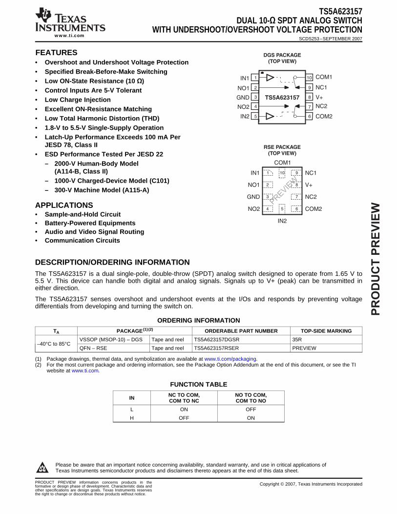
PRODUCT PREVIEW 1FEATURES APPLICATIONS IN2 DGS PACKAGE (TOP VIEW) 1 2 3 4 5 10 9 8 7 6 IN1 NO1 GND NO2 V+ NC1 COM1 NC2 COM2 TS5A623157 NC1 V+ NC2 COM2 IN1 NO1 GND NO2 RSE PACKAGE (TOP VIEW) COM1 PREVIEW IN2 1 2 3 4 5 6 7 8 9 10 DESCRIPTION/ORDERING INFORMATION TS5A623157 DUAL 10-Ω SPDT ANALOG SWITCH WITH UNDERSHOOT/OVERSHOOT VOLTAGE PROTECTION SCDS253 – SEPTEMBER 2007 www.ti.com • Overshoot and Undershoot Voltage Protection • Specified Break-Before-Make Switching • Low ON-State Resistance (10 Ω) • Control Inputs Are 5-V Tolerant • Low Charge Injection • Excellent ON-Resistance Matching • Low Total Harmonic Distortion (THD) • 1.8-V to 5.5-V Single-Supply Operation • Latch-Up Performance Exceeds 100 mA Per JESD 78, Class II • ESD Performance Tested Per JESD 22 – 2000-V Human-Body Model (A114-B, Class II) – 1000-V Charged-Device Model (C101) – 300-V Machine Model (A115-A) • Sample-and-Hold Circuit • Battery-Powered Equipments • Audio and Video Signal Routing xxx • Communication Circuits xxx The TS5A623157 is a dual single-pole, double-throw (SPDT) analog switch designed to operate from 1.65 V to 5.5 V. This device can handle both digital and analog signals. Signals up to V+ (peak) can be transmitted in either direction. The TS5A623157 senses overshoot and undershoot events at the I/Os and responds by preventing voltage differentials from developing and turning the switch on. ORDERING INFORMATION T A PACKAGE (1) (2) ORDERABLE PART NUMBER TOP-SIDE MARKING VSSOP (MSOP-10) – DGS Tape and reel TS5A623157DGSR 35R –40°C to 85°C QFN – RSE Tape and reel TS5A623157RSER PREVIEW (1) Package drawings, thermal data, and symbolization are available at www.ti.com/packaging. (2) For the most current package and ordering information, see the Package Option Addendum at the end of this document, or see the TI website at www.ti.com. FUNCTION TABLE NC TO COM, NO TO COM, IN COM TO NC COM TO NO L ON OFF H OFF ON 1 Please be aware that an important notice concerning availability, standard warranty, and use in critical applications of Texas Instruments semiconductor products and disclaimers thereto appears at the end of this data sheet. PRODUCT PREVIEW information concerns products in the Copyright © 2007, Texas Instruments Incorporated formative or design phase of development. Characteristic data and other specifications are design goals. Texas Instruments reserves the right to change or discontinue these products without notice.
Transcript of Dual 10-Ohm SPDT Analog Switch With … PRODUCT PREVIEW Absolute Minimum and Maximum Ratings(1)(2)...
PR
OD
UC
T P
RE
VIE
W
1FEATURES
APPLICATIONS
IN2
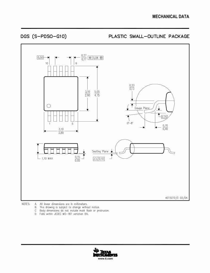
DGS PACKAGE
(TOP VIEW)
1
2
3
4
5
10
9
8
7
6
IN1
NO1
GND
NO2
V+
NC1
COM1
NC2
COM2
TS5A623157
NC1
V+
NC2
COM2
IN1
NO1
GND
NO2
RSE PACKAGE
(TOP VIEW)
COM1
PREVIE
W
IN2
1
2
3
4 5 6
7
8
910
DESCRIPTION/ORDERING INFORMATION
TS5A623157DUAL 10-Ω SPDT ANALOG SWITCH
WITH UNDERSHOOT/OVERSHOOT VOLTAGE PROTECTIONSCDS253–SEPTEMBER 2007
www.ti.com
• Overshoot and Undershoot Voltage Protection• Specified Break-Before-Make Switching• Low ON-State Resistance (10 Ω)• Control Inputs Are 5-V Tolerant• Low Charge Injection• Excellent ON-Resistance Matching• Low Total Harmonic Distortion (THD)• 1.8-V to 5.5-V Single-Supply Operation• Latch-Up Performance Exceeds 100 mA Per
JESD 78, Class II• ESD Performance Tested Per JESD 22
– 2000-V Human-Body Model(A114-B, Class II)
– 1000-V Charged-Device Model (C101)– 300-V Machine Model (A115-A)
• Sample-and-Hold Circuit• Battery-Powered Equipments• Audio and Video Signal Routing
xxx
• Communication Circuitsxxx
The TS5A623157 is a dual single-pole, double-throw (SPDT) analog switch designed to operate from 1.65 V to5.5 V. This device can handle both digital and analog signals. Signals up to V+ (peak) can be transmitted ineither direction.
The TS5A623157 senses overshoot and undershoot events at the I/Os and responds by preventing voltagedifferentials from developing and turning the switch on.
ORDERING INFORMATION
TA PACKAGE (1) (2) ORDERABLE PART NUMBER TOP-SIDE MARKING
VSSOP (MSOP-10) – DGS Tape and reel TS5A623157DGSR 35R–40°C to 85°C
QFN – RSE Tape and reel TS5A623157RSER PREVIEW
(1) Package drawings, thermal data, and symbolization are available at www.ti.com/packaging.(2) For the most current package and ordering information, see the Package Option Addendum at the end of this document, or see the TI
website at www.ti.com.
FUNCTION TABLE
NC TO COM, NO TO COM,IN COM TO NC COM TO NO
L ON OFF
H OFF ON
1
Please be aware that an important notice concerning availability, standard warranty, and use in critical applications ofTexas Instruments semiconductor products and disclaimers thereto appears at the end of this data sheet.
PRODUCT PREVIEW information concerns products in the Copyright © 2007, Texas Instruments Incorporatedformative or design phase of development. Characteristic data andother specifications are design goals. Texas Instruments reservesthe right to change or discontinue these products without notice.
www.ti.com
PR
OD
UC
T P
RE
VIE
W
Absolute Minimum and Maximum Ratings (1) (2)
Package Thermal Impedance
TS5A623157DUAL 10-Ω SPDT ANALOG SWITCHWITH UNDERSHOOT/OVERSHOOT VOLTAGE PROTECTIONSCDS253–SEPTEMBER 2007
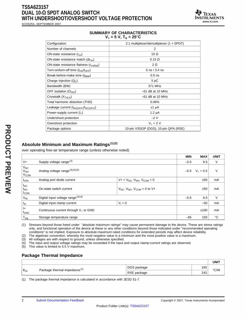
SUMMARY OF CHARACTERISTICSV+ = 5 V, TA = 25°C
Configuration 2:1 multiplexer/demultiplexer (1 × SPDT)
Number of channels 2
ON-state resistance (ron) 10 ΩON-state resistance match (Δron) 0.15 ΩON-state resistance flatness (ron(flat)) 2 ΩTurn-on/turn-off time (tON/tOFF) 5 ns / 3.4 ns
Break-before-make time (tBBM) 0.5 ns
Charge injection (QC) 5 pC
Bandwidth (BW) 371 MHz
OFF isolation (OISO) –61 dB at 10 MHz
Crosstalk (XTALK) –61 dB at 10 MHz
Total harmonic distortion (THD) 0.06%
Leakage current (INO(OFF)/INC(OFF)) ±1 μA
Power-supply current (I+) 1.2 μA
Undershoot protection –2 V
Overshoot protection V+ + 2 V
Package options 10-pin VSSOP (DGS), 10-pin QFN (RSE)
over operating free-air temperature range (unless otherwise noted)
MIN MAX UNIT
V+ Supply voltage range (3) –0.5 6.5 V
VNCVNO Analog voltage range (3) (4) (5) –0.5 V+ + 0.5 VVCOM
II/OK Analog port diode current V+ < VNC, VNO, VCOM < 0 ±50 mA
INCINO On-state switch current VNC, VNO, VCOM = 0 to V+ ±50 mAICOM
VIN Digital input voltage range (3) (4) –0.5 6.5 V
IIK Digital input clamp current VI < 0 –50 mA
I+ Continuous current through V+ or GND ±100 mAIGND
Tstg Storage temperature range –65 150 °C
(1) Stresses beyond those listed under "absolute maximum ratings" may cause permanent damage to the device. These are stress ratingsonly, and functional operation of the device at these or any other conditions beyond those indicated under "recommended operatingconditions" is not implied. Exposure to absolute-maximum-rated conditions for extended periods may affect device reliability.
(2) The algebraic convention, whereby the most negative value is a minimum and the most positive value is a maximum.(3) All voltages are with respect to ground, unless otherwise specified.(4) The input and output voltage ratings may be exceeded if the input and output clamp-current ratings are observed.(5) This value is limited to 5.5 V maximum.
UNIT
DGS package 165θJA Package thermal impedance (1) °C/W
RSE package 243
(1) The package thermal impedance is calculated in accordance with JESD 51-7.
2 Submit Documentation Feedback Copyright © 2007, Texas Instruments Incorporated
Product Folder Link(s): TS5A623157
www.ti.com
PR
OD
UC
T P
RE
VIE
W
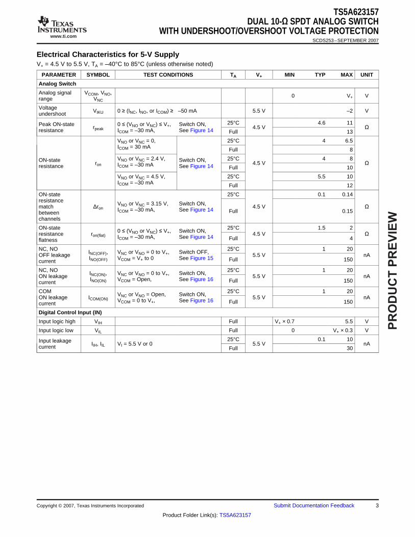
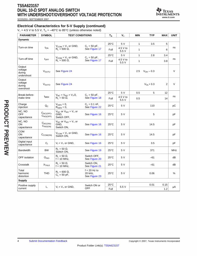
Electrical Characteristics for 5-V Supply
TS5A623157DUAL 10-Ω SPDT ANALOG SWITCH
WITH UNDERSHOOT/OVERSHOOT VOLTAGE PROTECTIONSCDS253–SEPTEMBER 2007
V+ = 4.5 V to 5.5 V, TA = –40°C to 85°C (unless otherwise noted)
PARAMETER SYMBOL TEST CONDITIONS TA V+ MIN TYP MAX UNIT
Analog Switch
Analog signal VCOM, VNO, 0 V+ Vrange VNC
Voltage VIKU 0 ≥ (INC, INO, or ICOM) ≥ –50 mA 5.5 V –2 Vundershoot
25°C 4.6 11Peak ON-state 0 ≤ (VNO or VNC) ≤ V+, Switch ON,rpeak 4.5 V Ωresistance ICOM = –30 mA, See Figure 14 Full 13
VNO or VNC = 0, 25°C 4 6.5ICOM = 30 mA Full 8
VNO or VNC = 2.4 V, 25°C 4 8ON-state Switch ON,ron 4.5 V ΩICOM = –30 mAresistance See Figure 14 Full 10
VNO or VNC = 4.5 V, 25°C 5.5 10ICOM = –30 mA Full 12
ON-state 25°C 0.1 0.14resistance VNO or VNC = 3.15 V, Switch ON,match Δron 4.5 V ΩICOM = –30 mA, See Figure 14 Full 0.15betweenchannels
ON-state 25°C 1.5 20 ≤ (VNO or VNC) ≤ V+, Switch ON,resistance ron(flat) 4.5 V ΩICOM = –30 mA, See Figure 14 Full 4flatness
NC, NO 25°C 1 20INC(OFF), VNC or VNO = 0 to V+, Switch OFF,OFF leakage 5.5 V nAINO(OFF) VCOM = V+ to 0 See Figure 15 Full 150current
NC, NO 25°C 1 20INC(ON), VNC or VNO = 0 to V+, Switch ON,ON leakage 5.5 V nAINO(ON) VCOM = Open, See Figure 16 Full 150current
COM 25°C 1 20VNC or VNO = Open, Switch ON,ON leakage ICOM(ON) 5.5 V nAVCOM = 0 to V+, See Figure 16 Full 150current
Digital Control Input (IN)
Input logic high VIH Full V+ × 0.7 5.5 V
Input logic low VIL Full 0 V+ × 0.3 V
25°C 0.1 10Input leakage IIH, IIL VI = 5.5 V or 0 5.5 V nAcurrent Full 30
Copyright © 2007, Texas Instruments Incorporated Submit Documentation Feedback 3
Product Folder Link(s): TS5A623157
www.ti.com
PR
OD
UC
T P
RE
VIE
W
TS5A623157DUAL 10-Ω SPDT ANALOG SWITCHWITH UNDERSHOOT/OVERSHOOT VOLTAGE PROTECTIONSCDS253–SEPTEMBER 2007
Electrical Characteristics for 5-V Supply (continued)V+ = 4.5 V to 5.5 V, TA = –40°C to 85°C (unless otherwise noted)
PARAMETER SYMBOL TEST CONDITIONS TA V+ MIN TYP MAX UNIT
Dynamic
25°C 5 V 1 3.5 5VCOM = V+ or GND, CL = 50 pF,Turn-on time tON ns4.5 V toRL = 500 Ω, See Figure 17 Full 1 65.5 V
25°C 5 V 1 2.8 3.4VCOM = V+ or GND, CL = 50 pF,Turn-off time tOFF ns4.5 V toRL = 500 Ω, See Figure 17 Full 1 3.85.5 V
Outputvoltage VOUTU See Figure 24 2.5 VOH – 0.3 Vduringundershoot
Outputvoltage VOUTO See Figure 24 VOL+ 0.3 2 Vduringovershoot
25°C 5 V 0.5 5 12Break-before- VNC = VNO = V+/2, CL = 50 pF,tBBM ns4.5 V tomake time RL = 50 Ω, See Figure 18 Full 0.5 145.5 V
Charge VGEN = 0, CL = 0.1 nF,QC 25°C 5 V 110 pCinjection RGEN = 0, See Figure 22
NC, NO VNC or VNO = V+ orCNC(OFF),OFF GND, See Figure 16 25°C 5 V 5 pFCNO(OFF)capacitance Switch OFF,
NC, NO VNC or VNO = V+ orCNC(ON),ON GND, See Figure 16 25°C 5 V 14.5 pFCNO(ON)capacitance Switch ON,
COM VCOM = V+ or GND,ON CCOM(ON) See Figure 16 25°C 5 V 14.5 pFSwitch ON,capacitance
Digital input CI VI = V+ or GND, See Figure 16 25°C 5 V 3.5 pFcapacitance
RL = 50 Ω,Bandwidth BW See Figure 19 25°C 5 V 371 MHzSwitch ON,
RL = 50 Ω, Switch OFF,OFF isolation OISO 25°C 5 V –61 dBf = 10 MHz, See Figure 20
RL = 50 Ω, Switch ON,Crosstalk XTALK 25°C 5 V –61 dBf = 10 MHz, See Figure 21
Total f = 20 Hz toRL = 600 Ω,harmonic THD 20 kHz, 25°C 5 V 0.06 %CL = 50 pF,distortion See Figure 23
Supply
25°C 0.01 0.15Positive supply Switch ON orI+ VI = V+ or GND, 5.5 V μAcurrent OFF Full 1.2
4 Submit Documentation Feedback Copyright © 2007, Texas Instruments Incorporated
Product Folder Link(s): TS5A623157
www.ti.com
PR
OD
UC
T P
RE
VIE
W
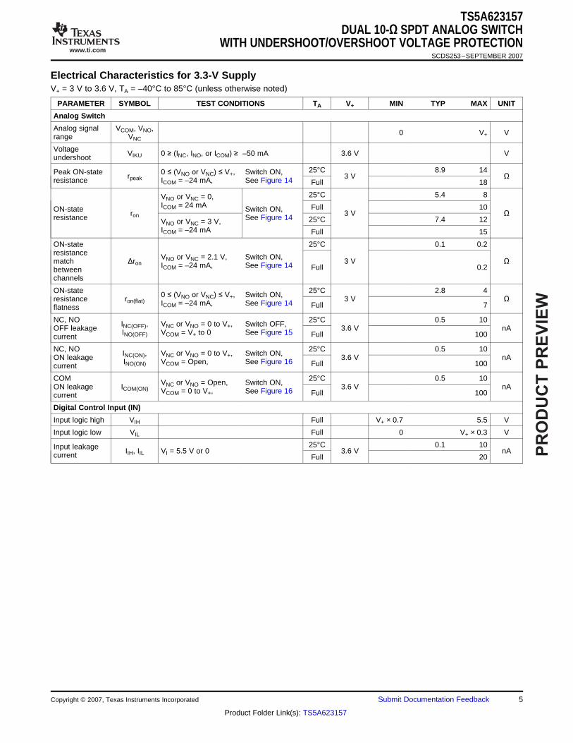
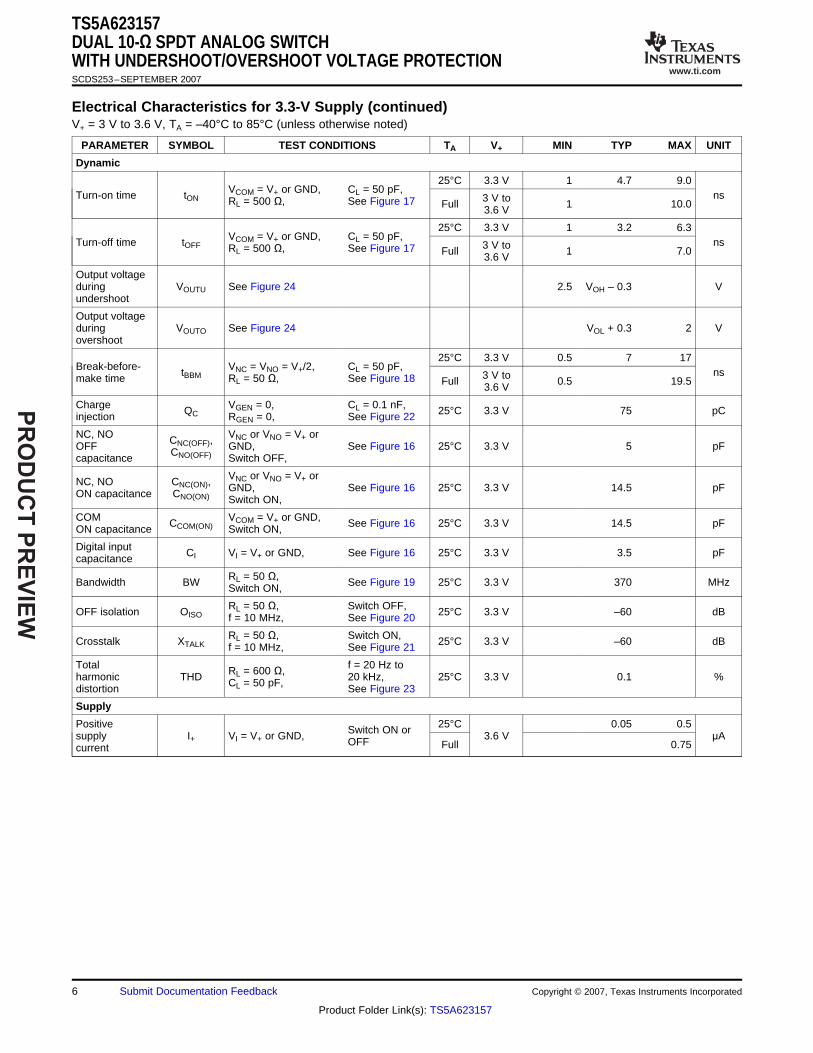
Electrical Characteristics for 3.3-V Supply
TS5A623157DUAL 10-Ω SPDT ANALOG SWITCH
WITH UNDERSHOOT/OVERSHOOT VOLTAGE PROTECTIONSCDS253–SEPTEMBER 2007
V+ = 3 V to 3.6 V, TA = –40°C to 85°C (unless otherwise noted)
PARAMETER SYMBOL TEST CONDITIONS TA V+ MIN TYP MAX UNIT
Analog Switch
Analog signal VCOM, VNO, 0 V+ Vrange VNC
Voltage VIKU 0 ≥ (INC, INO, or ICOM) ≥ –50 mA 3.6 V Vundershoot
25°C 8.9 14Peak ON-state 0 ≤ (VNO or VNC) ≤ V+, Switch ON,rpeak 3 V Ωresistance ICOM = –24 mA, See Figure 14 Full 18
25°C 5.4 8VNO or VNC = 0,ICOM = 24 mA Full 10ON-state Switch ON,ron 3 V Ωresistance See Figure 14 25°C 7.4 12VNO or VNC = 3 V,ICOM = –24 mA Full 15
ON-state 25°C 0.1 0.2resistance VNO or VNC = 2.1 V, Switch ON,match Δron 3 V ΩICOM = –24 mA, See Figure 14 Full 0.2betweenchannels
ON-state 25°C 2.8 40 ≤ (VNO or VNC) ≤ V+, Switch ON,resistance ron(flat) 3 V ΩICOM = –24 mA, See Figure 14 Full 7flatness
NC, NO 25°C 0.5 10INC(OFF), VNC or VNO = 0 to V+, Switch OFF,OFF leakage 3.6 V nAINO(OFF) VCOM = V+ to 0 See Figure 15 Full 100current
NC, NO 25°C 0.5 10INC(ON), VNC or VNO = 0 to V+, Switch ON,ON leakage 3.6 V nAINO(ON) VCOM = Open, See Figure 16 Full 100current
COM 25°C 0.5 10VNC or VNO = Open, Switch ON,ON leakage ICOM(ON) 3.6 V nAVCOM = 0 to V+, See Figure 16 Full 100current
Digital Control Input (IN)
Input logic high VIH Full V+ × 0.7 5.5 V
Input logic low VIL Full 0 V+ × 0.3 V
25°C 0.1 10Input leakage IIH, IIL VI = 5.5 V or 0 3.6 V nAcurrent Full 20
Copyright © 2007, Texas Instruments Incorporated Submit Documentation Feedback 5
Product Folder Link(s): TS5A623157
www.ti.com
PR
OD
UC
T P
RE
VIE
W
TS5A623157DUAL 10-Ω SPDT ANALOG SWITCHWITH UNDERSHOOT/OVERSHOOT VOLTAGE PROTECTIONSCDS253–SEPTEMBER 2007
Electrical Characteristics for 3.3-V Supply (continued)V+ = 3 V to 3.6 V, TA = –40°C to 85°C (unless otherwise noted)
PARAMETER SYMBOL TEST CONDITIONS TA V+ MIN TYP MAX UNIT
Dynamic
25°C 3.3 V 1 4.7 9.0VCOM = V+ or GND, CL = 50 pF,Turn-on time tON ns3 V toRL = 500 Ω, See Figure 17 Full 1 10.03.6 V
25°C 3.3 V 1 3.2 6.3VCOM = V+ or GND, CL = 50 pF,Turn-off time tOFF ns3 V toRL = 500 Ω, See Figure 17 Full 1 7.03.6 V
Output voltageduring VOUTU See Figure 24 2.5 VOH – 0.3 Vundershoot
Output voltageduring VOUTO See Figure 24 VOL + 0.3 2 Vovershoot
25°C 3.3 V 0.5 7 17Break-before- VNC = VNO = V+/2, CL = 50 pF,tBBM ns3 V tomake time RL = 50 Ω, See Figure 18 Full 0.5 19.53.6 V
Charge VGEN = 0, CL = 0.1 nF,QC 25°C 3.3 V 75 pCinjection RGEN = 0, See Figure 22
NC, NO VNC or VNO = V+ orCNC(OFF),OFF GND, See Figure 16 25°C 3.3 V 5 pFCNO(OFF)capacitance Switch OFF,
VNC or VNO = V+ orNC, NO CNC(ON), GND, See Figure 16 25°C 3.3 V 14.5 pFON capacitance CNO(ON) Switch ON,
COM VCOM = V+ or GND,CCOM(ON) See Figure 16 25°C 3.3 V 14.5 pFON capacitance Switch ON,
Digital input CI VI = V+ or GND, See Figure 16 25°C 3.3 V 3.5 pFcapacitance
RL = 50 Ω,Bandwidth BW See Figure 19 25°C 3.3 V 370 MHzSwitch ON,
RL = 50 Ω, Switch OFF,OFF isolation OISO 25°C 3.3 V –60 dBf = 10 MHz, See Figure 20
RL = 50 Ω, Switch ON,Crosstalk XTALK 25°C 3.3 V –60 dBf = 10 MHz, See Figure 21
Total f = 20 Hz toRL = 600 Ω,harmonic THD 20 kHz, 25°C 3.3 V 0.1 %CL = 50 pF,distortion See Figure 23
Supply
Positive 25°C 0.05 0.5Switch ON orsupply I+ VI = V+ or GND, 3.6 V μAOFF Full 0.75current
6 Submit Documentation Feedback Copyright © 2007, Texas Instruments Incorporated
Product Folder Link(s): TS5A623157
www.ti.com
PR
OD
UC
T P
RE
VIE
W
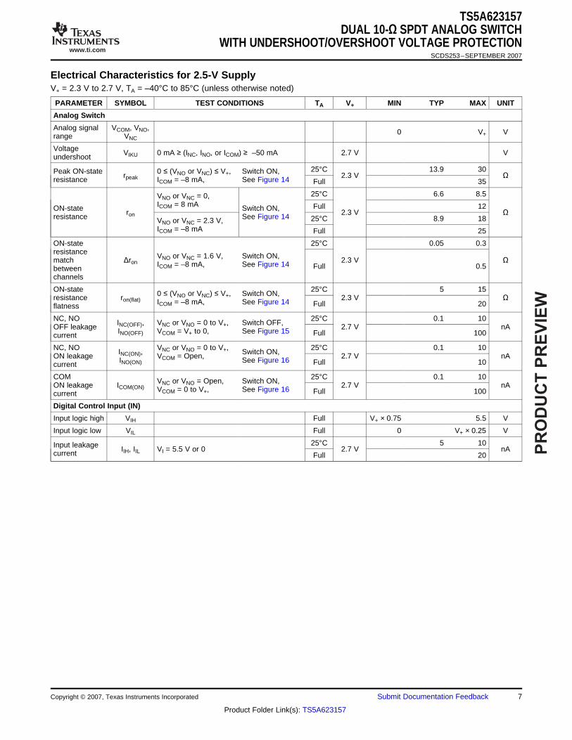
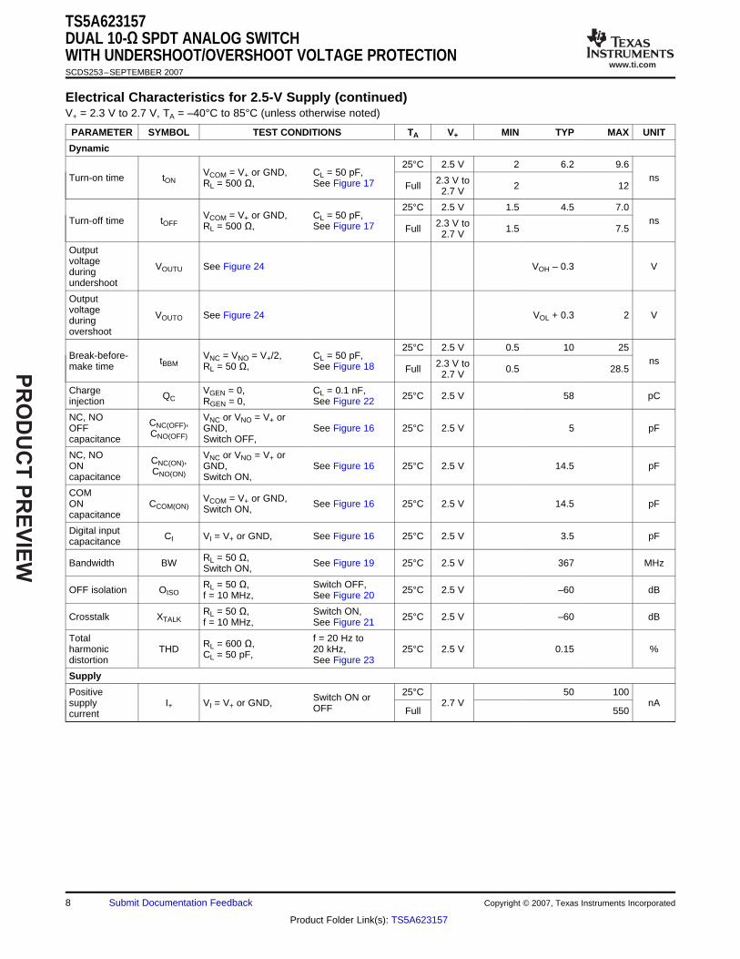
Electrical Characteristics for 2.5-V Supply
TS5A623157DUAL 10-Ω SPDT ANALOG SWITCH
WITH UNDERSHOOT/OVERSHOOT VOLTAGE PROTECTIONSCDS253–SEPTEMBER 2007
V+ = 2.3 V to 2.7 V, TA = –40°C to 85°C (unless otherwise noted)
PARAMETER SYMBOL TEST CONDITIONS TA V+ MIN TYP MAX UNIT
Analog Switch
Analog signal VCOM, VNO, 0 V+ Vrange VNC
Voltage VIKU 0 mA ≥ (INC, INO, or ICOM) ≥ –50 mA 2.7 V Vundershoot
25°C 13.9 30Peak ON-state 0 ≤ (VNO or VNC) ≤ V+, Switch ON,rpeak 2.3 V Ωresistance ICOM = –8 mA, See Figure 14 Full 35
25°C 6.6 8.5VNO or VNC = 0,ICOM = 8 mA Full 12ON-state Switch ON,ron 2.3 V Ωresistance See Figure 14 25°C 8.9 18VNO or VNC = 2.3 V,ICOM = –8 mA Full 25
ON-state 25°C 0.05 0.3resistance VNO or VNC = 1.6 V, Switch ON,match Δron 2.3 V ΩICOM = –8 mA, See Figure 14 Full 0.5betweenchannels
ON-state 25°C 5 150 ≤ (VNO or VNC) ≤ V+, Switch ON,resistance ron(flat) 2.3 V ΩICOM = –8 mA, See Figure 14 Full 20flatness
NC, NO 25°C 0.1 10INC(OFF), VNC or VNO = 0 to V+, Switch OFF,OFF leakage 2.7 V nAINO(OFF) VCOM = V+ to 0, See Figure 15 Full 100current
NC, NO VNC or VNO = 0 to V+, 25°C 0.1 10INC(ON), Switch ON,ON leakage VCOM = Open, 2.7 V nAINO(ON) See Figure 16 Full 10current
COM 25°C 0.1 10VNC or VNO = Open, Switch ON,ON leakage ICOM(ON) 2.7 V nAVCOM = 0 to V+, See Figure 16 Full 100current
Digital Control Input (IN)
Input logic high VIH Full V+ × 0.75 5.5 V
Input logic low VIL Full 0 V+ × 0.25 V
25°C 5 10Input leakage IIH, IIL VI = 5.5 V or 0 2.7 V nAcurrent Full 20
Copyright © 2007, Texas Instruments Incorporated Submit Documentation Feedback 7
Product Folder Link(s): TS5A623157
www.ti.com
PR
OD
UC
T P
RE
VIE
W
TS5A623157DUAL 10-Ω SPDT ANALOG SWITCHWITH UNDERSHOOT/OVERSHOOT VOLTAGE PROTECTIONSCDS253–SEPTEMBER 2007
Electrical Characteristics for 2.5-V Supply (continued)V+ = 2.3 V to 2.7 V, TA = –40°C to 85°C (unless otherwise noted)
PARAMETER SYMBOL TEST CONDITIONS TA V+ MIN TYP MAX UNIT
Dynamic
25°C 2.5 V 2 6.2 9.6VCOM = V+ or GND, CL = 50 pF,Turn-on time tON ns2.3 V toRL = 500 Ω, See Figure 17 Full 2 122.7 V
25°C 2.5 V 1.5 4.5 7.0VCOM = V+ or GND, CL = 50 pF,Turn-off time tOFF ns2.3 V toRL = 500 Ω, See Figure 17 Full 1.5 7.52.7 V
Outputvoltage VOUTU See Figure 24 VOH – 0.3 Vduringundershoot
Outputvoltage VOUTO See Figure 24 VOL + 0.3 2 Vduringovershoot
25°C 2.5 V 0.5 10 25Break-before- VNC = VNO = V+/2, CL = 50 pF,tBBM ns2.3 V tomake time RL = 50 Ω, See Figure 18 Full 0.5 28.52.7 V
Charge VGEN = 0, CL = 0.1 nF,QC 25°C 2.5 V 58 pCinjection RGEN = 0, See Figure 22
NC, NO VNC or VNO = V+ orCNC(OFF),OFF GND, See Figure 16 25°C 2.5 V 5 pFCNO(OFF)capacitance Switch OFF,
NC, NO VNC or VNO = V+ orCNC(ON),ON GND, See Figure 16 25°C 2.5 V 14.5 pFCNO(ON)capacitance Switch ON,
COM VCOM = V+ or GND,ON CCOM(ON) See Figure 16 25°C 2.5 V 14.5 pFSwitch ON,capacitance
Digital input CI VI = V+ or GND, See Figure 16 25°C 2.5 V 3.5 pFcapacitance
RL = 50 Ω,Bandwidth BW See Figure 19 25°C 2.5 V 367 MHzSwitch ON,
RL = 50 Ω, Switch OFF,OFF isolation OISO 25°C 2.5 V –60 dBf = 10 MHz, See Figure 20
RL = 50 Ω, Switch ON,Crosstalk XTALK 25°C 2.5 V –60 dBf = 10 MHz, See Figure 21
Total f = 20 Hz toRL = 600 Ω,harmonic THD 20 kHz, 25°C 2.5 V 0.15 %CL = 50 pF,distortion See Figure 23
Supply
Positive 25°C 50 100Switch ON orsupply I+ VI = V+ or GND, 2.7 V nAOFF Full 550current
8 Submit Documentation Feedback Copyright © 2007, Texas Instruments Incorporated
Product Folder Link(s): TS5A623157
www.ti.com
PR
OD
UC
T P
RE
VIE
W
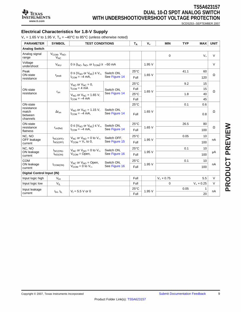
Electrical Characteristics for 1.8-V Supply
TS5A623157DUAL 10-Ω SPDT ANALOG SWITCH
WITH UNDERSHOOT/OVERSHOOT VOLTAGE PROTECTIONSCDS253–SEPTEMBER 2007
V+ = 1.65 V to 1.95 V, TA = –40°C to 85°C (unless otherwise noted)
PARAMETER SYMBOL TEST CONDITIONS TA V+ MIN TYP MAX UNIT
Analog Switch
Analog signal VCOM, VNO, 0 V+ Vrange VNC
Voltage VIKU 0 ≥ (INC, INO, or ICOM) ≥ –50 mA 1.95 V Vundershoot
Peak 25°C 41.1 600 ≤ (VNO or VNC) ≤ V+, Switch ON,ON-state rpeak 1.65 V ΩICOM = –4 mA, See Figure 14 Full 120resistance
25°C 9.2 15VNO or VNC = 0,ICOM = 4 mA Full 15ON-state Switch ON,ron 1.65 V Ωresistance See Figure 14 25°C 1.8 40VNO or VNC = 1.65 V,ICOM = –4 mA Full 45
ON-state 25°C 0.1 0.6resistance VNO or VNC = 1.15 V, Switch ON,match Δron 1.65 V ΩICOM = –4 mA, See Figure 14 Full 0.8betweenchannels
ON-state 25°C 26.5 800 ≤ (VNO or VNC) ≤ V+, Switch ON,resistance ron(flat) 1.65 V ΩICOM = –4 mA, See Figure 14 Full 100flatness
NC, NO 25°C 0.05 10INC(OFF), VNC or VNO = 0 to V+, Switch OFF,OFF leakage 1.95 V nAINO(OFF) VCOM = V+ to 0, See Figure 15 Full 100current
NC, NO 25°C 0.1 10INC(ON), VNC or VNO = 0 to V+, Switch ON,ON leakage 1.95 V μAINO(ON) VCOM = Open, See Figure 16 Full 100current
COM 25°C 0.1 10VNC or VNO = Open, Switch ON,ON leakage ICOM(ON) 1.95 V nAVCOM = 0 to V+, See Figure 16 Full 100current
Digital Control Input (IN)
Input logic high VIH Full V+ × 0.75 5.5 V
Input logic low VIL Full 0 V+ × 0.25 V
25°C 0.05 1Input leakage IIH, IIL VI = 5.5 V or 0 1.95 V nAcurrent Full 20
Copyright © 2007, Texas Instruments Incorporated Submit Documentation Feedback 9
Product Folder Link(s): TS5A623157
www.ti.com
PR
OD
UC
T P
RE
VIE
W
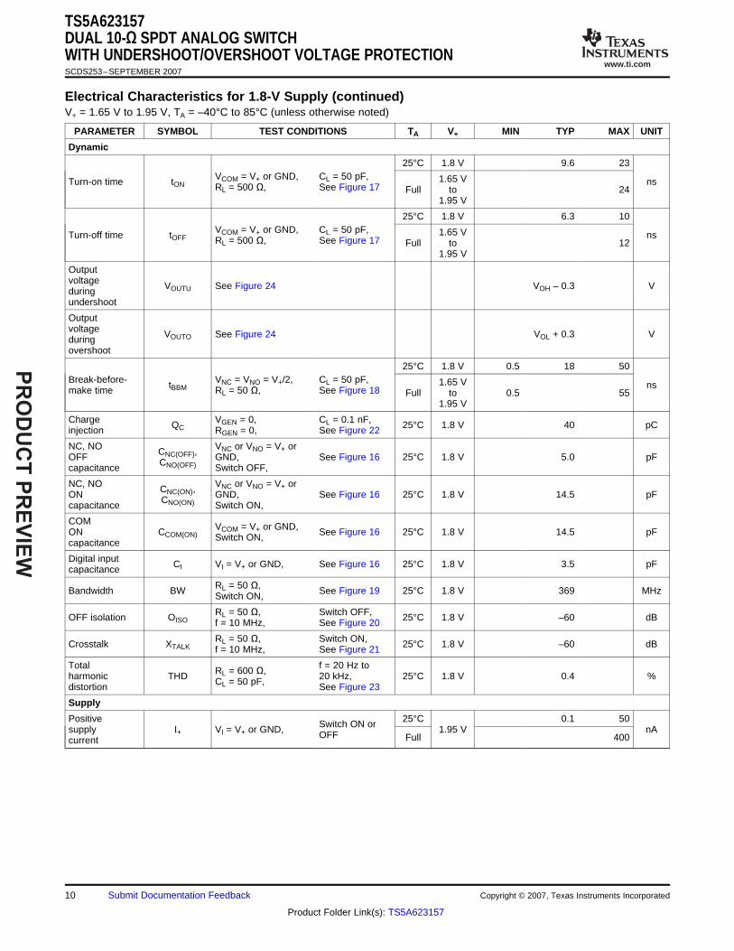
TS5A623157DUAL 10-Ω SPDT ANALOG SWITCHWITH UNDERSHOOT/OVERSHOOT VOLTAGE PROTECTIONSCDS253–SEPTEMBER 2007
Electrical Characteristics for 1.8-V Supply (continued)V+ = 1.65 V to 1.95 V, TA = –40°C to 85°C (unless otherwise noted)
PARAMETER SYMBOL TEST CONDITIONS TA V+ MIN TYP MAX UNIT
Dynamic
25°C 1.8 V 9.6 23VCOM = V+ or GND, CL = 50 pF, 1.65 VTurn-on time tON nsRL = 500 Ω, See Figure 17 Full to 24
1.95 V
25°C 1.8 V 6.3 10VCOM = V+ or GND, CL = 50 pF, 1.65 VTurn-off time tOFF nsRL = 500 Ω, See Figure 17 Full to 12
1.95 V
Outputvoltage VOUTU See Figure 24 VOH – 0.3 Vduringundershoot
Outputvoltage VOUTO See Figure 24 VOL + 0.3 Vduringovershoot
25°C 1.8 V 0.5 18 50Break-before- VNC = VNO = V+/2, CL = 50 pF, 1.65 VtBBM nsmake time RL = 50 Ω, See Figure 18 Full to 0.5 55
1.95 V
Charge VGEN = 0, CL = 0.1 nF,QC 25°C 1.8 V 40 pCinjection RGEN = 0, See Figure 22
NC, NO VNC or VNO = V+ orCNC(OFF),OFF GND, See Figure 16 25°C 1.8 V 5.0 pFCNO(OFF)capacitance Switch OFF,
NC, NO VNC or VNO = V+ orCNC(ON),ON GND, See Figure 16 25°C 1.8 V 14.5 pFCNO(ON)capacitance Switch ON,
COM VCOM = V+ or GND,ON CCOM(ON) See Figure 16 25°C 1.8 V 14.5 pFSwitch ON,capacitance
Digital input CI VI = V+ or GND, See Figure 16 25°C 1.8 V 3.5 pFcapacitance
RL = 50 Ω,Bandwidth BW See Figure 19 25°C 1.8 V 369 MHzSwitch ON,
RL = 50 Ω, Switch OFF,OFF isolation OISO 25°C 1.8 V –60 dBf = 10 MHz, See Figure 20
RL = 50 Ω, Switch ON,Crosstalk XTALK 25°C 1.8 V –60 dBf = 10 MHz, See Figure 21
Total f = 20 Hz toRL = 600 Ω,harmonic THD 20 kHz, 25°C 1.8 V 0.4 %CL = 50 pF,distortion See Figure 23
Supply
Positive 25°C 0.1 50Switch ON orsupply I+ VI = V+ or GND, 1.95 V nAOFF Full 400current
10 Submit Documentation Feedback Copyright © 2007, Texas Instruments Incorporated
Product Folder Link(s): TS5A623157
www.ti.com
PR
OD
UC
T P
RE
VIE
W
TS5A623157DUAL 10-Ω SPDT ANALOG SWITCH
WITH UNDERSHOOT/OVERSHOOT VOLTAGE PROTECTIONSCDS253–SEPTEMBER 2007
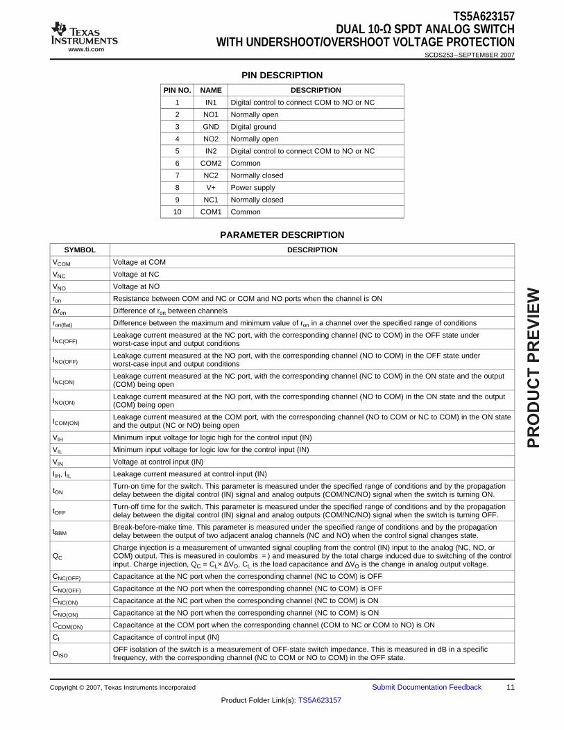
PIN DESCRIPTION
PIN NO. NAME DESCRIPTION
1 IN1 Digital control to connect COM to NO or NC
2 NO1 Normally open
3 GND Digital ground
4 NO2 Normally open
5 IN2 Digital control to connect COM to NO or NC
6 COM2 Common
7 NC2 Normally closed
8 V+ Power supply
9 NC1 Normally closed
10 COM1 Common
PARAMETER DESCRIPTION
SYMBOL DESCRIPTION
VCOM Voltage at COM
VNC Voltage at NC
VNO Voltage at NO
ron Resistance between COM and NC or COM and NO ports when the channel is ON
Δron Difference of ron between channels
ron(flat) Difference between the maximum and minimum value of ron in a channel over the specified range of conditions
Leakage current measured at the NC port, with the corresponding channel (NC to COM) in the OFF state underINC(OFF) worst-case input and output conditions
Leakage current measured at the NO port, with the corresponding channel (NO to COM) in the OFF state underINO(OFF) worst-case input and output conditions
Leakage current measured at the NC port, with the corresponding channel (NC to COM) in the ON state and the outputINC(ON) (COM) being open
Leakage current measured at the NO port, with the corresponding channel (NO to COM) in the ON state and the outputINO(ON) (COM) being open
Leakage current measured at the COM port, with the corresponding channel (NO to COM or NC to COM) in the ON stateICOM(ON) and the output (NC or NO) being open
VIH Minimum input voltage for logic high for the control input (IN)
VIL Minimum input voltage for logic low for the control input (IN)
VIN Voltage at control input (IN)
IIH, IIL Leakage current measured at control input (IN)
Turn-on time for the switch. This parameter is measured under the specified range of conditions and by the propagationtON delay between the digital control (IN) signal and analog outputs (COM/NC/NO) signal when the switch is turning ON.
Turn-off time for the switch. This parameter is measured under the specified range of conditions and by the propagationtOFF delay between the digital control (IN) signal and analog outputs (COM/NC/NO) signal when the switch is turning OFF.
Break-before-make time. This parameter is measured under the specified range of conditions and by the propagationtBBM delay between the output of two adjacent analog channels (NC and NO) when the control signal changes state.
Charge injection is a measurement of unwanted signal coupling from the control (IN) input to the analog (NC, NO, orQC COM) output. This is measured in coulombs =) and measured by the total charge induced due to switching of the control
input. Charge injection, QC = CL× ΔVO, CL is the load capacitance and ΔVO is the change in analog output voltage.
CNC(OFF) Capacitance at the NC port when the corresponding channel (NC to COM) is OFF
CNO(OFF) Capacitance at the NO port when the corresponding channel (NC to COM) is OFF
CNC(ON) Capacitance at the NC port when the corresponding channel (NC to COM) is ON
CNO(ON) Capacitance at the NO port when the corresponding channel (NC to COM) is ON
CCOM(ON) Capacitance at the COM port when the corresponding channel (COM to NC or COM to NO) is ON
CI Capacitance of control input (IN)
OFF isolation of the switch is a measurement of OFF-state switch impedance. This is measured in dB in a specificOISO frequency, with the corresponding channel (NC to COM or NO to COM) in the OFF state.
Copyright © 2007, Texas Instruments Incorporated Submit Documentation Feedback 11
Product Folder Link(s): TS5A623157
www.ti.com
PR
OD
UC
T P
RE
VIE
W
TS5A623157DUAL 10-Ω SPDT ANALOG SWITCHWITH UNDERSHOOT/OVERSHOOT VOLTAGE PROTECTIONSCDS253–SEPTEMBER 2007
PARAMETER DESCRIPTION (continued)
SYMBOL DESCRIPTION
Crosstalk is a measurement of unwanted signal coupling from an ON channel to an OFF channel (NC to NO or NO toXTALK NC). This is measured at a specific frequency and in dB.
BW Bandwidth of the switch. This is the frequency where the gain of an ON channel is –3 dB below the dc gain.
Total harmonic distortion is defined as the ratio of the root mean square (RMS) value of the second, third, and higherTHD harmonics to the magnitude of fundamental harmonic.
I+ Static power-supply current with the control (IN) pin at V+ or GND
Output voltage during an undershoot event. This is measured by turning off a specific channel and applying anVOUTU undershoot voltage at the input of the switch.
Output voltage during an overshoot event. This is measured by turning off a specific channel and applying an overshootVOUTO voltage at the input of the switch.
12 Submit Documentation Feedback Copyright © 2007, Texas Instruments Incorporated
Product Folder Link(s): TS5A623157
www.ti.com
PR
OD
UC
T P
RE
VIE
W
TYPICAL CHARACTERISTICS
V (V)COM
r(
)on
Ω
0
2
4
6
8
10
12
0.0 0.5 1.0 1.5 2.0 2.5 3.0
–40°C
25°C
85°C
0
10
20
30
40
50
60
0 1 2 3 4 5
V (V)COM
r(
)on
Ω
1.8 V
2.5 V
3.3 V
5.0 V
0.0
0.5
1.0
1.5
2.0
2.5
3.0
3.5
–40 25 85
T (°C)A
Leakage C
urr
ent (n
A)
COM (ON)
NC/NO (ON)
NC/NO (OFF)
V (V)COM
r(
)o
nΩ
0
1
2
3
4
5
6
7
8
9
0 1 2 3 4 5
–40°C
25°C
85°C
0
2
4
6
8
10
12
0 1 2 3 4 5 6
V (V)+
t/t
(ns)
ON
OF
F
tON
tOFF
–150
–100
–50
0
50
100
150
0 1 2 3 4 5 6
V (V)bias
Q(p
C)
C
1.8 V
2.5 V
3.3 V
5.0 V
TS5A623157DUAL 10-Ω SPDT ANALOG SWITCH
WITH UNDERSHOOT/OVERSHOOT VOLTAGE PROTECTIONSCDS253–SEPTEMBER 2007
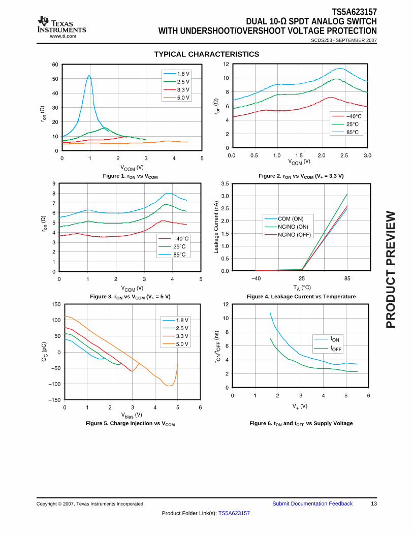
Figure 1. rON vs VCOM Figure 2. rON vs VCOM (V+ = 3.3 V)
Figure 3. rON vs VCOM (V+ = 5 V) Figure 4. Leakage Current vs Temperature
Figure 5. Charge Injection vs VCOM Figure 6. tON and tOFF vs Supply Voltage
Copyright © 2007, Texas Instruments Incorporated Submit Documentation Feedback 13
Product Folder Link(s): TS5A623157
www.ti.com
PR
OD
UC
T P
RE
VIE
W
0
1
2
3
4
–40 25 85
T (°C)A
t/t
(ns)
ON
OF
F
tON
tOFF
0.0
0.5
1.0
1.5
2.0
2.5
0 1 2 3 4 5 6
V (V)+
Lo
gic
-Level T
hre
sh
old
(V
)
V RisingIN
VIN Falling
0.00
0.05
0.10
0.15
0.20
0.25
0.30
0.35
10 100 1000 10000 100000
Frequency (Hz)
TH
D+
(%
)1.8 V
2.5 V
3.3 V
5.0 V
–18
–16
–14
–12
–10
–8
–6
–4
–2
0
Frequency (Hz)
Gain
(d
b)
1.8 V ±0.35 V
2.5 V 0.35 V±
3.3 V 0.35 V±
5 V 0.35 V±
0.0E+00 2.0E+08 4.0E+08 6.0E+08 8.0E+08 1.0E+09 1.2E+09
–90
–80
–70
–60
–50
–40
–30
–20
–10
0
0.0E+00 2.0E+08 4.0E+08 6.0E+08 8.0E+08 1.0E+09 1.2E+09
Frequency (Hz)
Attenuation (
dB
)
1.8 V
2.5 V
3.3 V
5.0 V
0.0E+00 2.0E+08 4.0E+08 6.0E+08 8.0E+08 1.0E+09 1.2E+09Frequency (Hz)
-100
-90
-80
-70
-60
-50
-40
-30
-20
-10
0
Att
en
ua
tio
n (
dB
)
1.8 V
2.5 V
3.3 V
5.0 V
TS5A623157DUAL 10-Ω SPDT ANALOG SWITCHWITH UNDERSHOOT/OVERSHOOT VOLTAGE PROTECTIONSCDS253–SEPTEMBER 2007
TYPICAL CHARACTERISTICS (continued)
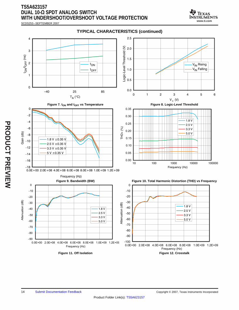
Figure 7. tON and tOFF vs Temperature Figure 8. Logic-Level Threshold
Figure 9. Bandwidth (BW) Figure 10. Total Harmonic Distortion (THD) vs Frequency
Figure 11. Off Isolation Figure 12. Crosstalk
14 Submit Documentation Feedback Copyright © 2007, Texas Instruments Incorporated
Product Folder Link(s): TS5A623157
www.ti.com
PR
OD
UC
T P
RE
VIE
W
–0.1
0.0
0.1
0.2
0.3
0.4
0.5
0.6
0.7
0.8
0.0 1.0 2.0 3.0 4.0 5.0 6.0
V (V)CC
I(
A)
CC
μ25 C°
85 C°
– °40 C
TS5A623157DUAL 10-Ω SPDT ANALOG SWITCH
WITH UNDERSHOOT/OVERSHOOT VOLTAGE PROTECTIONSCDS253–SEPTEMBER 2007
TYPICAL CHARACTERISTICS (continued)
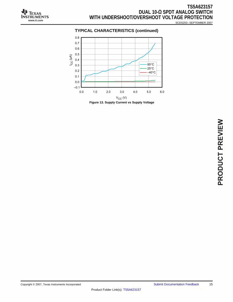
Figure 13. Supply Current vs Supply Voltage
Copyright © 2007, Texas Instruments Incorporated Submit Documentation Feedback 15
Product Folder Link(s): TS5A623157
www.ti.com
PR
OD
UC
T P
RE
VIE
W
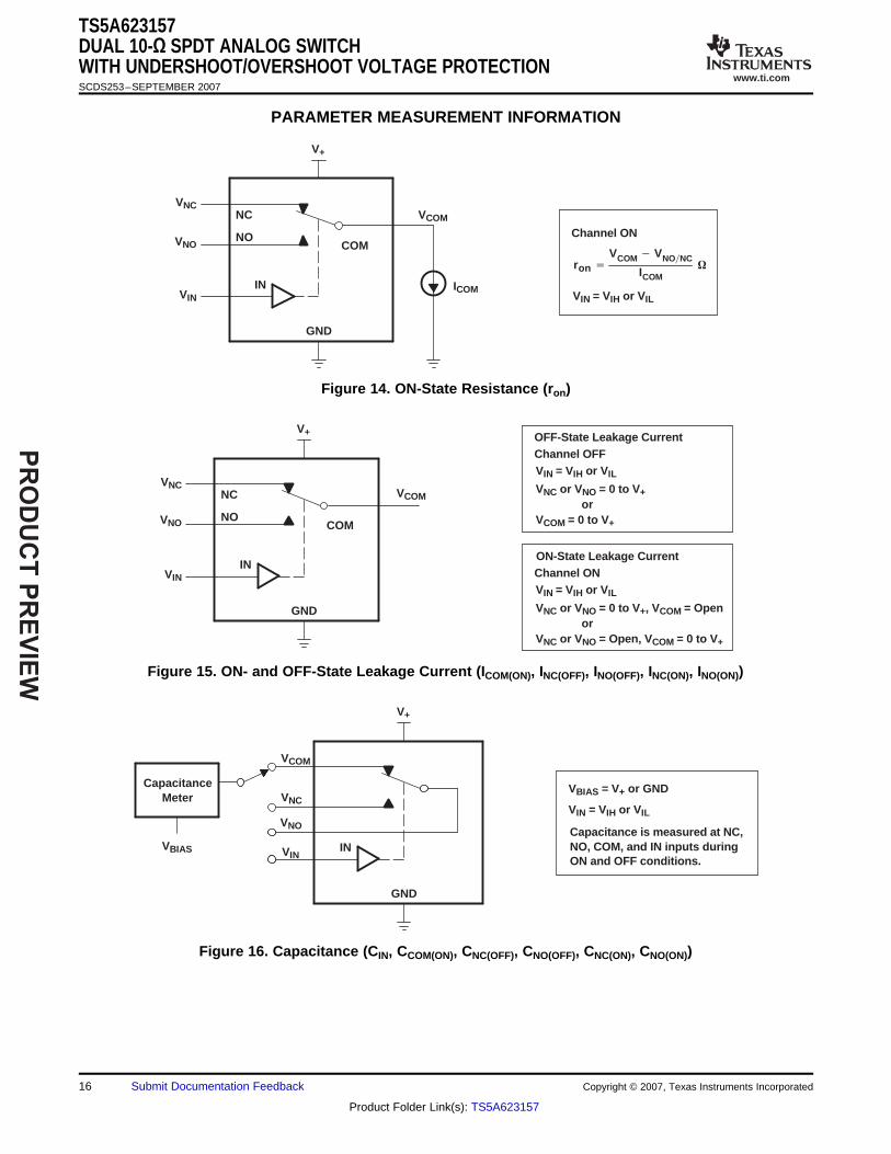
PARAMETER MEASUREMENT INFORMATION
V+
ICOM
ron VCOM VNONC
ICOM
GND
Channel ON
NC
INVIN
NOCOM
VCOM
VIN = VIH or VIL
VNO
VNC
V+
GND
Channel OFF
NC
IN
VNC
VIN
NOCOM
VCOM
VCOM = 0 to V+
OFF-State Leakage Current
or
VIN = VIH or V IL
VNC or VNO = 0 to V+
Channel ON
VNC or VNO = Open, VCOM = 0 to V+
ON-State Leakage Current
or
VIN = VIH or V IL
VNC or VNO = 0 to V+, VCOM = Open
VNO
V+
GND
INVBIAS VIN
VIN = VIH or VIL
VBIAS = V+ or GND
Capacitance is measured at NC,NO, COM, and IN inputs duringON and OFF conditions.
CapacitanceMeter
VNO
VNC
VCOM
TS5A623157DUAL 10-Ω SPDT ANALOG SWITCHWITH UNDERSHOOT/OVERSHOOT VOLTAGE PROTECTIONSCDS253–SEPTEMBER 2007
Figure 14. ON-State Resistance (ron)
Figure 15. ON- and OFF-State Leakage Current (ICOM(ON), INC(OFF), INO(OFF), INC(ON), INO(ON))
Figure 16. Capacitance (CIN, CCOM(ON), CNC(OFF), CNO(OFF), CNC(ON), CNO(ON))
16 Submit Documentation Feedback Copyright © 2007, Texas Instruments Incorporated
Product Folder Link(s): TS5A623157
www.ti.com
PR
OD
UC
T P
RE
VIE
W
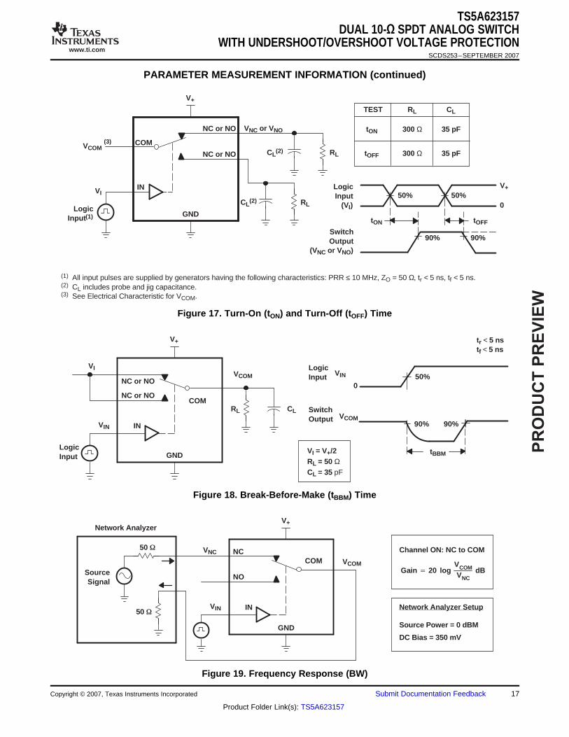
CL(2) RLVCOM
V+
GND
NC or NO VNC or VNO
VI
NC or NO
COM
LogicInput(1)
300 Ω
RL CL
35 pFtON
TEST
300 Ω 35 pFtOFF
50%
tON tOFF
50%
90% 90%
LogicInput
(VI)
V+
SwitchOutput
(VNC or VNO)
0CL(2) RL
IN
(3)
(1) All input pulses are supplied by generators having the following characteristics: PRR ≤ 10 MHz, ZO = 50 Ω, tr < 5 ns, tf < 5 ns.(2) CL includes probe and jig capacitance.(3) See Electrical Characteristic for VCOM.
V+
GND
NC or NO
IN
VI
VIN
NC or NOCOM
VCOM
RL CLVCOM
tBBM
050%
90% 90%
VIN
tr < 5 nstf < 5 ns
VI = V+/2RL = 50 ΩCL = 35 pF
LogicInput
LogicInput
SwitchOutput
V+
GND
NC
INVIN
NO
COM
50
50
VNC
VCOMGain 20 log
VCOMVNC
dB
Channel ON: NC to COM
Network Analyzer Setup
Source Power = 0 dBM
DC Bias = 350 mV
Network Analyzer
SourceSignal
TS5A623157DUAL 10-Ω SPDT ANALOG SWITCH
WITH UNDERSHOOT/OVERSHOOT VOLTAGE PROTECTIONSCDS253–SEPTEMBER 2007
PARAMETER MEASUREMENT INFORMATION (continued)
Figure 17. Turn-On (tON) and Turn-Off (tOFF) Time
Figure 18. Break-Before-Make (tBBM) Time
Figure 19. Frequency Response (BW)
Copyright © 2007, Texas Instruments Incorporated Submit Documentation Feedback 17
Product Folder Link(s): TS5A623157
www.ti.com
PR
OD
UC
T P
RE
VIE
W
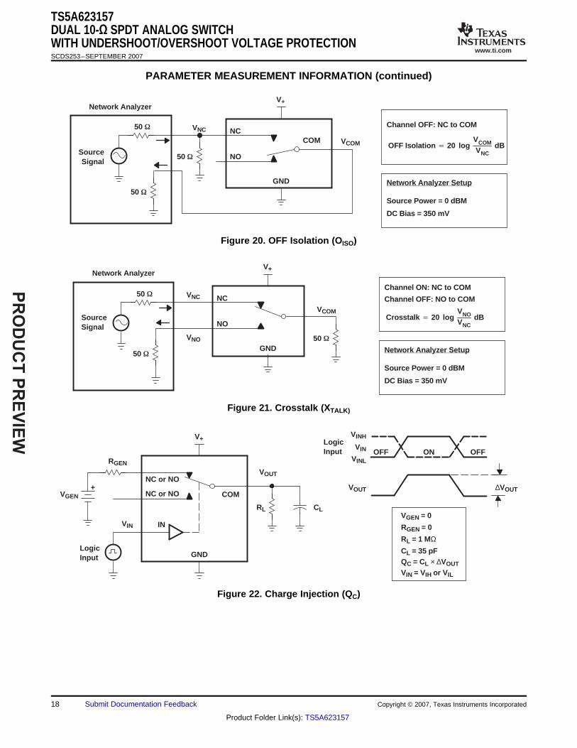
NC
NO
COM
VNC
VCOM OFF Isolation 20 logVCOMVNC
dB
Channel OFF: NC to COM
Network Analyzer Setup
Source Power = 0 dBM
DC Bias = 350 mV
50
V+
GND
50
50
Network Analyzer
SourceSignal
NC
NO
50
50
VNC
VCOMCrosstalk 20 log
VNOVNC
dB
Channel ON: NC to COM
Network Analyzer Setup
Source Power = 0 dBM
DC Bias = 350 mV
50
V+
GNDVNO
SourceSignal
Channel OFF: NO to COM
Network Analyzer
V+
GND
NC or NO
IN
RGEN
VIN
NC or NO COM
VOUT
RL CL
OFFVIN
VOUT
ON OFF
∆VOUTVGEN
+
VIN = VIH or VIL
RL = 1 MΩCL = 35 pF
VGEN = 0
RGEN = 0
QC = CL × ∆VOUT
LogicInput
VINH
VINL
LogicInput
TS5A623157DUAL 10-Ω SPDT ANALOG SWITCHWITH UNDERSHOOT/OVERSHOOT VOLTAGE PROTECTIONSCDS253–SEPTEMBER 2007
PARAMETER MEASUREMENT INFORMATION (continued)
Figure 20. OFF Isolation (OISO)
Figure 21. Crosstalk (XTALK)
Figure 22. Charge Injection (QC)
18 Submit Documentation Feedback Copyright © 2007, Texas Instruments Incorporated
Product Folder Link(s): TS5A623157
www.ti.com
PR
OD
UC
T P
RE
VIE
W
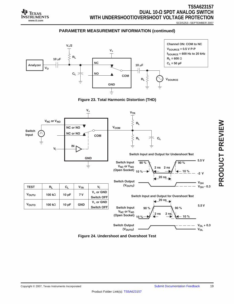
V+
GND
NC
NOCOM
10 F
RL
CL
RL = 600 ΩCL = 50 pF
VSOURCE = 0.5 V P-P
fSOURCE = 600 Hz to 20 kHzRL
VSOURCE
V+/2
Analyzer
10 F
Channel ON: COM to NC
VO
VTRRL CL
V+ or GND
VI
VOUTU
TEST
VOUTO
CLRL
7 V100 kΩ 10 pFSwitch OFF
GND100 kΩ 10 pF
-2 V
5.5 V
10 %
20 ns
10 %
90 % 90 %
2 ns 2 ns
VOH - 0.3
VOHSwitch Output
(VOUTU)
Switch Input
VNC or VNO
(Open Socket)
VOL
VOL + 0.3Switch Output
(VOUTO)
V+ or GND
Switch OFF
V+
GND
NC or NO
IN
VNC or VNO
VI
COM
VCOM
Switch
Input
RL
VTR
NC or NO
Switch Input and Output for Undershoot Test
Switch Input and Output for Overshoot Test
5.5 V
10 %
20 ns
10 %
90 % 90 %
2 ns 2 ns
Switch Input
VNC or VNO
(Open Socket)
TS5A623157DUAL 10-Ω SPDT ANALOG SWITCH
WITH UNDERSHOOT/OVERSHOOT VOLTAGE PROTECTIONSCDS253–SEPTEMBER 2007
PARAMETER MEASUREMENT INFORMATION (continued)
Figure 23. Total Harmonic Distortion (THD)
Figure 24. Undershoot and Overshoot Test
Copyright © 2007, Texas Instruments Incorporated Submit Documentation Feedback 19
Product Folder Link(s): TS5A623157
PACKAGE OPTION ADDENDUM
www.ti.com 25-Jul-2013
Addendum-Page 1
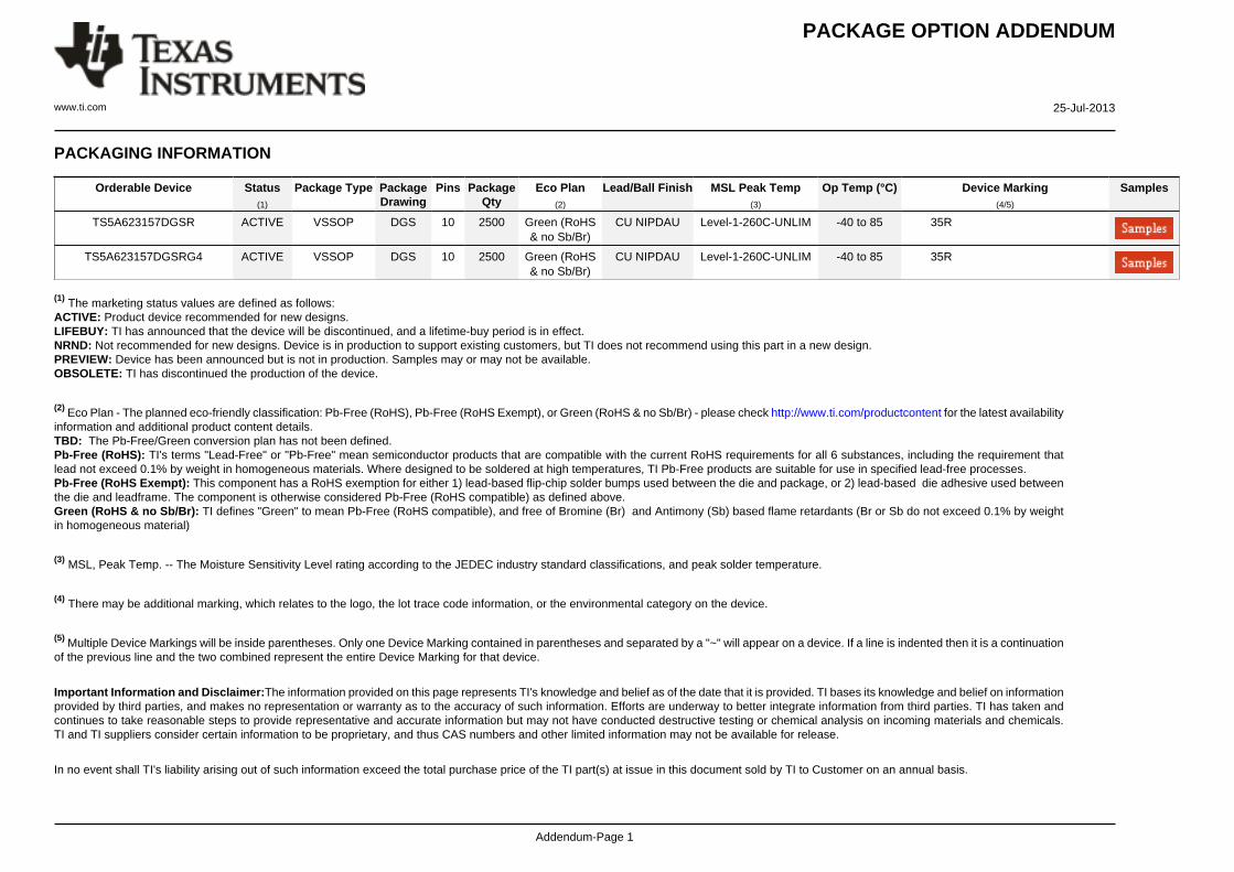
PACKAGING INFORMATION
Orderable Device Status(1)
Package Type PackageDrawing
Pins PackageQty
Eco Plan(2)
Lead/Ball Finish MSL Peak Temp(3)
Op Temp (°C) Device Marking(4/5)
Samples
TS5A623157DGSR ACTIVE VSSOP DGS 10 2500 Green (RoHS& no Sb/Br)
CU NIPDAU Level-1-260C-UNLIM -40 to 85 35R
TS5A623157DGSRG4 ACTIVE VSSOP DGS 10 2500 Green (RoHS& no Sb/Br)
CU NIPDAU Level-1-260C-UNLIM -40 to 85 35R
(1) The marketing status values are defined as follows:ACTIVE: Product device recommended for new designs.LIFEBUY: TI has announced that the device will be discontinued, and a lifetime-buy period is in effect.NRND: Not recommended for new designs. Device is in production to support existing customers, but TI does not recommend using this part in a new design.PREVIEW: Device has been announced but is not in production. Samples may or may not be available.OBSOLETE: TI has discontinued the production of the device.
(2) Eco Plan - The planned eco-friendly classification: Pb-Free (RoHS), Pb-Free (RoHS Exempt), or Green (RoHS & no Sb/Br) - please check http://www.ti.com/productcontent for the latest availabilityinformation and additional product content details.TBD: The Pb-Free/Green conversion plan has not been defined.Pb-Free (RoHS): TI's terms "Lead-Free" or "Pb-Free" mean semiconductor products that are compatible with the current RoHS requirements for all 6 substances, including the requirement thatlead not exceed 0.1% by weight in homogeneous materials. Where designed to be soldered at high temperatures, TI Pb-Free products are suitable for use in specified lead-free processes.Pb-Free (RoHS Exempt): This component has a RoHS exemption for either 1) lead-based flip-chip solder bumps used between the die and package, or 2) lead-based die adhesive used betweenthe die and leadframe. The component is otherwise considered Pb-Free (RoHS compatible) as defined above.Green (RoHS & no Sb/Br): TI defines "Green" to mean Pb-Free (RoHS compatible), and free of Bromine (Br) and Antimony (Sb) based flame retardants (Br or Sb do not exceed 0.1% by weightin homogeneous material)
(3) MSL, Peak Temp. -- The Moisture Sensitivity Level rating according to the JEDEC industry standard classifications, and peak solder temperature.
(4) There may be additional marking, which relates to the logo, the lot trace code information, or the environmental category on the device.
(5) Multiple Device Markings will be inside parentheses. Only one Device Marking contained in parentheses and separated by a "~" will appear on a device. If a line is indented then it is a continuationof the previous line and the two combined represent the entire Device Marking for that device.
Important Information and Disclaimer:The information provided on this page represents TI's knowledge and belief as of the date that it is provided. TI bases its knowledge and belief on informationprovided by third parties, and makes no representation or warranty as to the accuracy of such information. Efforts are underway to better integrate information from third parties. TI has taken andcontinues to take reasonable steps to provide representative and accurate information but may not have conducted destructive testing or chemical analysis on incoming materials and chemicals.TI and TI suppliers consider certain information to be proprietary, and thus CAS numbers and other limited information may not be available for release.
In no event shall TI's liability arising out of such information exceed the total purchase price of the TI part(s) at issue in this document sold by TI to Customer on an annual basis.
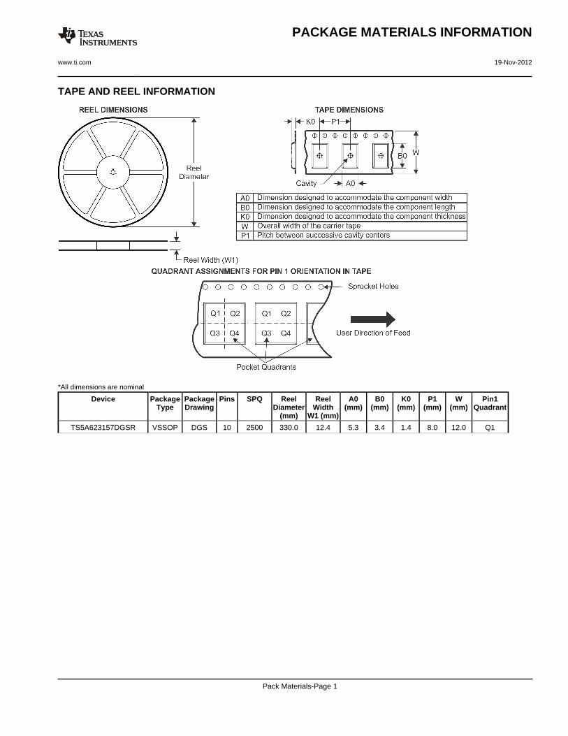
TAPE AND REEL INFORMATION
*All dimensions are nominal
Device PackageType
PackageDrawing
Pins SPQ ReelDiameter
(mm)
ReelWidth
W1 (mm)
A0(mm)
B0(mm)
K0(mm)
P1(mm)
W(mm)
Pin1Quadrant
TS5A623157DGSR VSSOP DGS 10 2500 330.0 12.4 5.3 3.4 1.4 8.0 12.0 Q1
PACKAGE MATERIALS INFORMATION
www.ti.com 19-Nov-2012
Pack Materials-Page 1
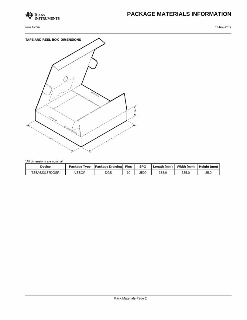
*All dimensions are nominal
Device Package Type Package Drawing Pins SPQ Length (mm) Width (mm) Height (mm)
TS5A623157DGSR VSSOP DGS 10 2500 358.0 335.0 35.0
PACKAGE MATERIALS INFORMATION
www.ti.com 19-Nov-2012
Pack Materials-Page 2
IMPORTANT NOTICE
Texas Instruments Incorporated and its subsidiaries (TI) reserve the right to make corrections, enhancements, improvements and otherchanges to its semiconductor products and services per JESD46, latest issue, and to discontinue any product or service per JESD48, latestissue. Buyers should obtain the latest relevant information before placing orders and should verify that such information is current andcomplete. All semiconductor products (also referred to herein as “components”) are sold subject to TI’s terms and conditions of salesupplied at the time of order acknowledgment.
TI warrants performance of its components to the specifications applicable at the time of sale, in accordance with the warranty in TI’s termsand conditions of sale of semiconductor products. Testing and other quality control techniques are used to the extent TI deems necessaryto support this warranty. Except where mandated by applicable law, testing of all parameters of each component is not necessarilyperformed.
TI assumes no liability for applications assistance or the design of Buyers’ products. Buyers are responsible for their products andapplications using TI components. To minimize the risks associated with Buyers’ products and applications, Buyers should provideadequate design and operating safeguards.
TI does not warrant or represent that any license, either express or implied, is granted under any patent right, copyright, mask work right, orother intellectual property right relating to any combination, machine, or process in which TI components or services are used. Informationpublished by TI regarding third-party products or services does not constitute a license to use such products or services or a warranty orendorsement thereof. Use of such information may require a license from a third party under the patents or other intellectual property of thethird party, or a license from TI under the patents or other intellectual property of TI.
Reproduction of significant portions of TI information in TI data books or data sheets is permissible only if reproduction is without alterationand is accompanied by all associated warranties, conditions, limitations, and notices. TI is not responsible or liable for such altereddocumentation. Information of third parties may be subject to additional restrictions.
Resale of TI components or services with statements different from or beyond the parameters stated by TI for that component or servicevoids all express and any implied warranties for the associated TI component or service and is an unfair and deceptive business practice.TI is not responsible or liable for any such statements.
Buyer acknowledges and agrees that it is solely responsible for compliance with all legal, regulatory and safety-related requirementsconcerning its products, and any use of TI components in its applications, notwithstanding any applications-related information or supportthat may be provided by TI. Buyer represents and agrees that it has all the necessary expertise to create and implement safeguards whichanticipate dangerous consequences of failures, monitor failures and their consequences, lessen the likelihood of failures that might causeharm and take appropriate remedial actions. Buyer will fully indemnify TI and its representatives against any damages arising out of the useof any TI components in safety-critical applications.
In some cases, TI components may be promoted specifically to facilitate safety-related applications. With such components, TI’s goal is tohelp enable customers to design and create their own end-product solutions that meet applicable functional safety standards andrequirements. Nonetheless, such components are subject to these terms.
No TI components are authorized for use in FDA Class III (or similar life-critical medical equipment) unless authorized officers of the partieshave executed a special agreement specifically governing such use.
Only those TI components which TI has specifically designated as military grade or “enhanced plastic” are designed and intended for use inmilitary/aerospace applications or environments. Buyer acknowledges and agrees that any military or aerospace use of TI componentswhich have not been so designated is solely at the Buyer's risk, and that Buyer is solely responsible for compliance with all legal andregulatory requirements in connection with such use.
TI has specifically designated certain components as meeting ISO/TS16949 requirements, mainly for automotive use. In any case of use ofnon-designated products, TI will not be responsible for any failure to meet ISO/TS16949.
Products Applications
Audio www.ti.com/audio Automotive and Transportation www.ti.com/automotive
Amplifiers amplifier.ti.com Communications and Telecom www.ti.com/communications
Data Converters dataconverter.ti.com Computers and Peripherals www.ti.com/computers
DLP® Products www.dlp.com Consumer Electronics www.ti.com/consumer-apps
DSP dsp.ti.com Energy and Lighting www.ti.com/energy
Clocks and Timers www.ti.com/clocks Industrial www.ti.com/industrial
Interface interface.ti.com Medical www.ti.com/medical
Logic logic.ti.com Security www.ti.com/security
Power Mgmt power.ti.com Space, Avionics and Defense www.ti.com/space-avionics-defense
Microcontrollers microcontroller.ti.com Video and Imaging www.ti.com/video
RFID www.ti-rfid.com
OMAP Applications Processors www.ti.com/omap TI E2E Community e2e.ti.com
Wireless Connectivity www.ti.com/wirelessconnectivity
Mailing Address: Texas Instruments, Post Office Box 655303, Dallas, Texas 75265Copyright © 2013, Texas Instruments Incorporated