Brief Introduction to H/W Design - AKABlog | Be The...
29
Brief Introduction to H/W Design
Transcript of Brief Introduction to H/W Design - AKABlog | Be The...
Brief Introduction to H/W Design
Table of Contents• Circuit Elements
• Circuit Analysis
• Digital VS Analog
• Application of Elements
• Block Diagram
• Design H/W System
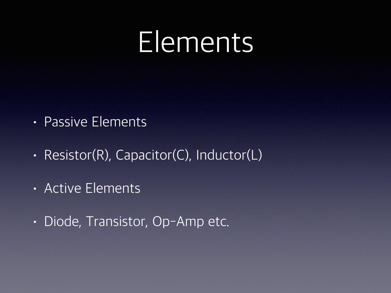
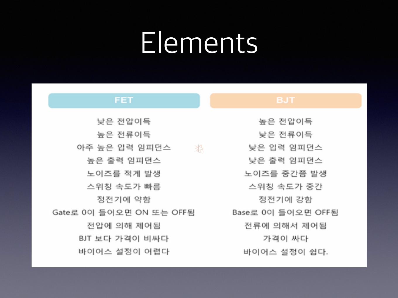
Elements
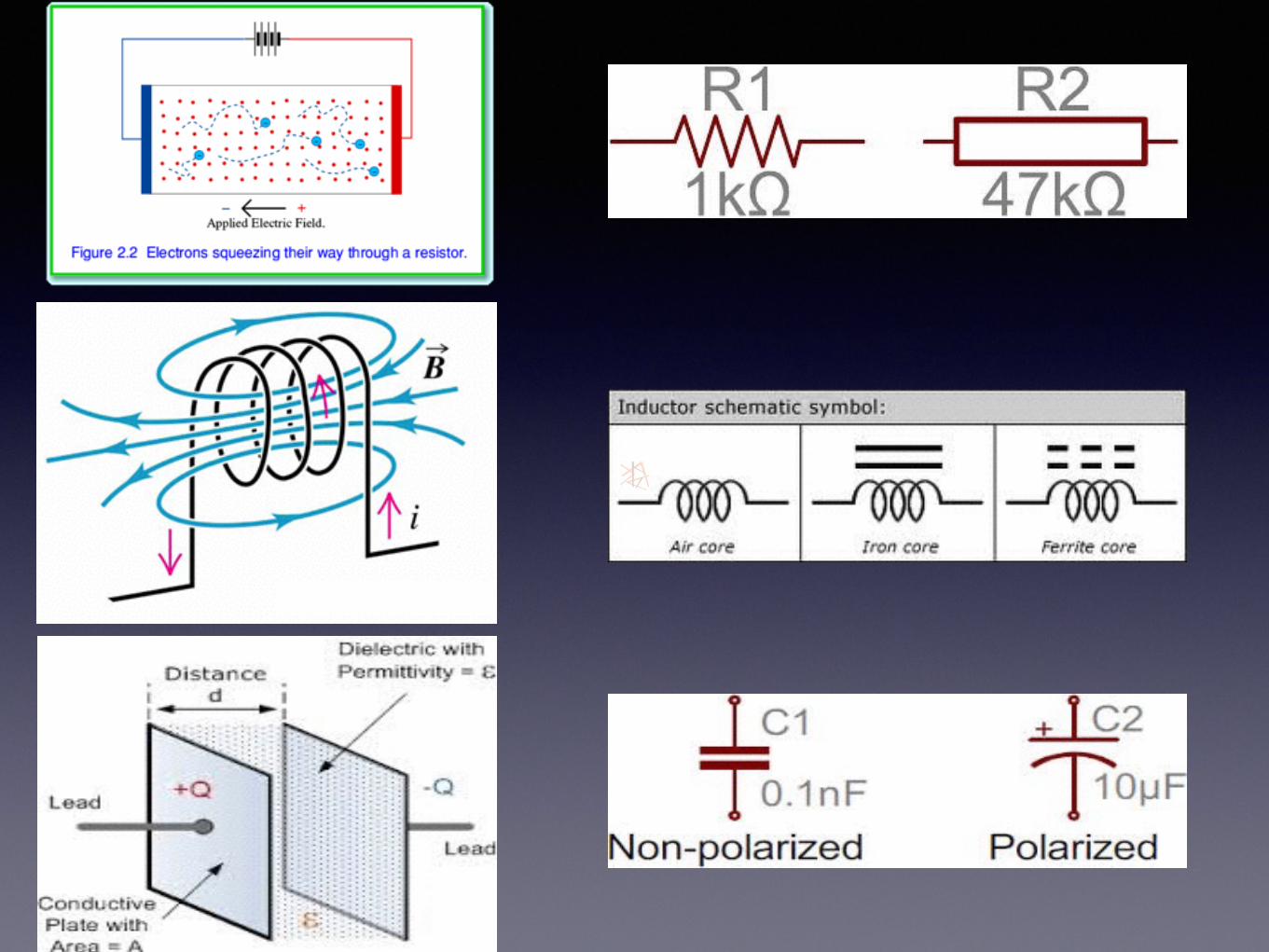
• Passive Elements
• Resistor(R), Capacitor(C), Inductor(L)
• Active Elements
• Diode, Transistor, Op-Amp etc.
Elements
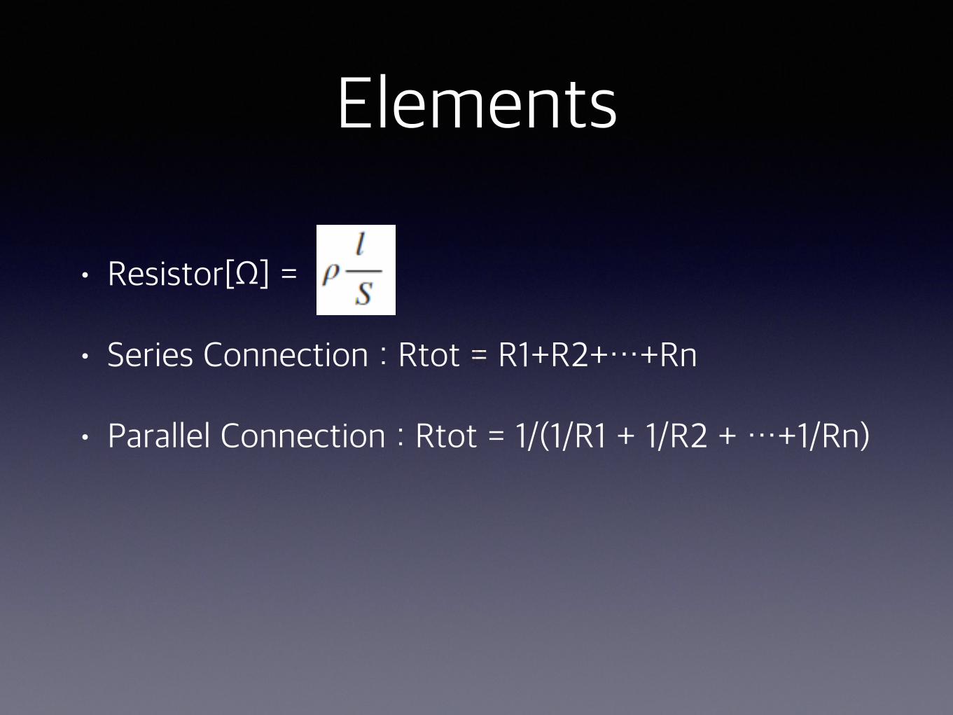
• Resistor[Ω] =
• Series Connection : Rtot = R1+R2+…+Rn
• Parallel Connection : Rtot = 1/(1/R1 + 1/R2 + …+1/Rn)
Elements
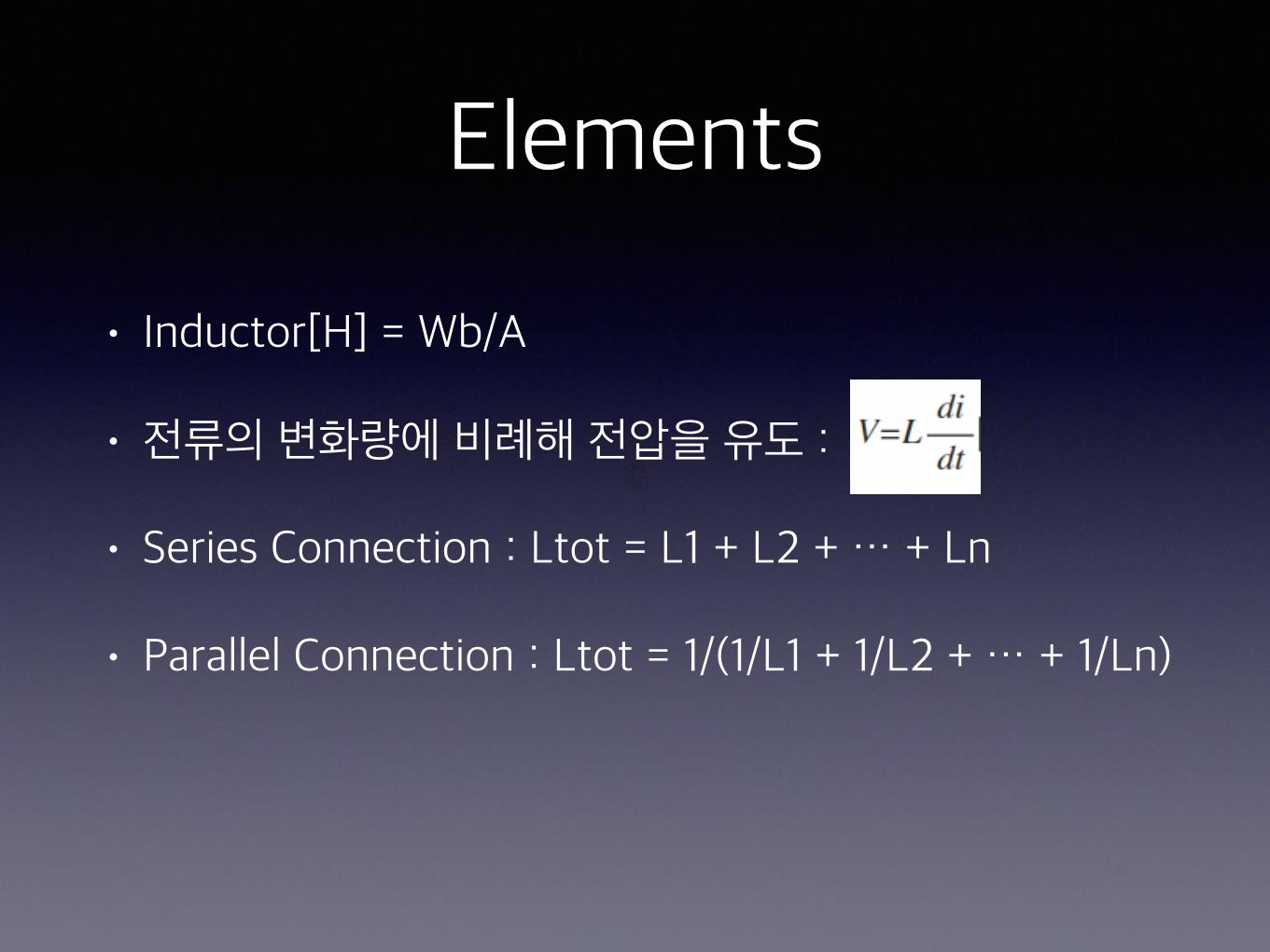
• Inductor[H] = Wb/A
• 전류의 변화량에 비례해 전압을 유도 :
• Series Connection : Ltot = L1 + L2 + … + Ln
• Parallel Connection : Ltot = 1/(1/L1 + 1/L2 + … + 1/Ln)
Elements
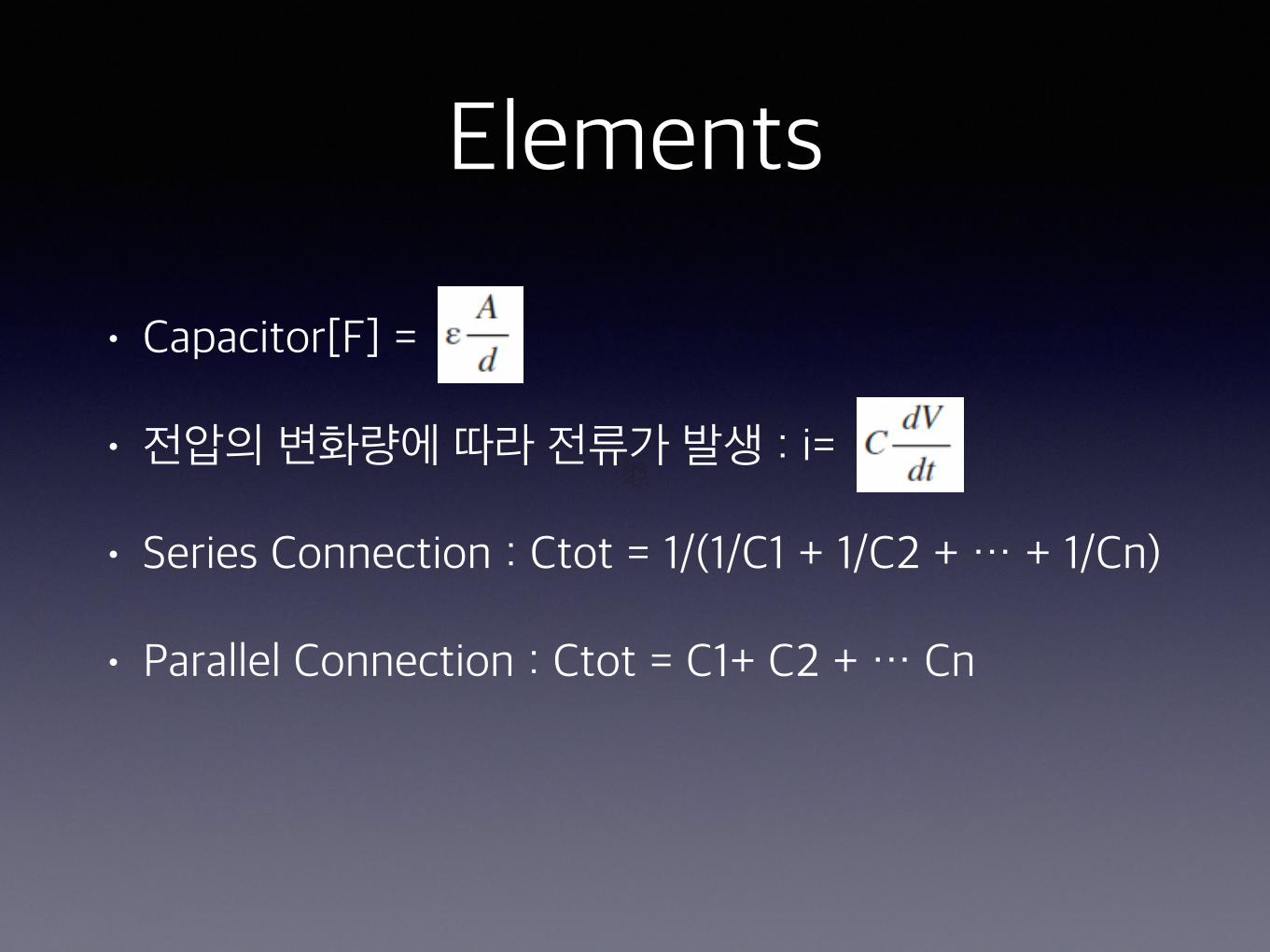
• Capacitor[F] =
• 전압의 변화량에 따라 전류가 발생 : i=
• Series Connection : Ctot = 1/(1/C1 + 1/C2 + … + 1/Cn)
• Parallel Connection : Ctot = C1+ C2 + … Cn
Elements
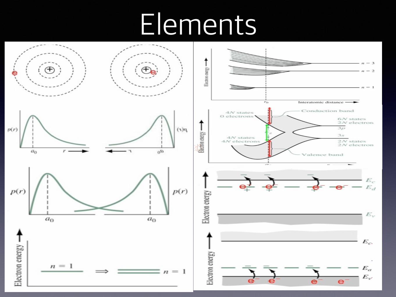
• Semiconductor
• In Periodic Table, Si is a very good element for making Semiconductors
• Semiconductors can have conductivity in specific conditions
• Si has four peripheral electrons
• 3족 원소 첨가시, P type Semiconductor 생성
• 5족 원소 첨가시, N type Semiconductor 생성
Elements
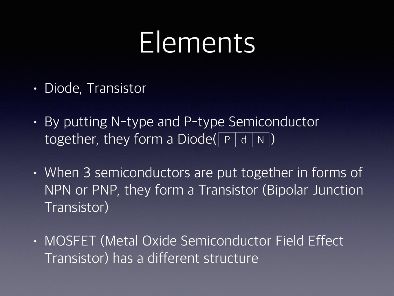
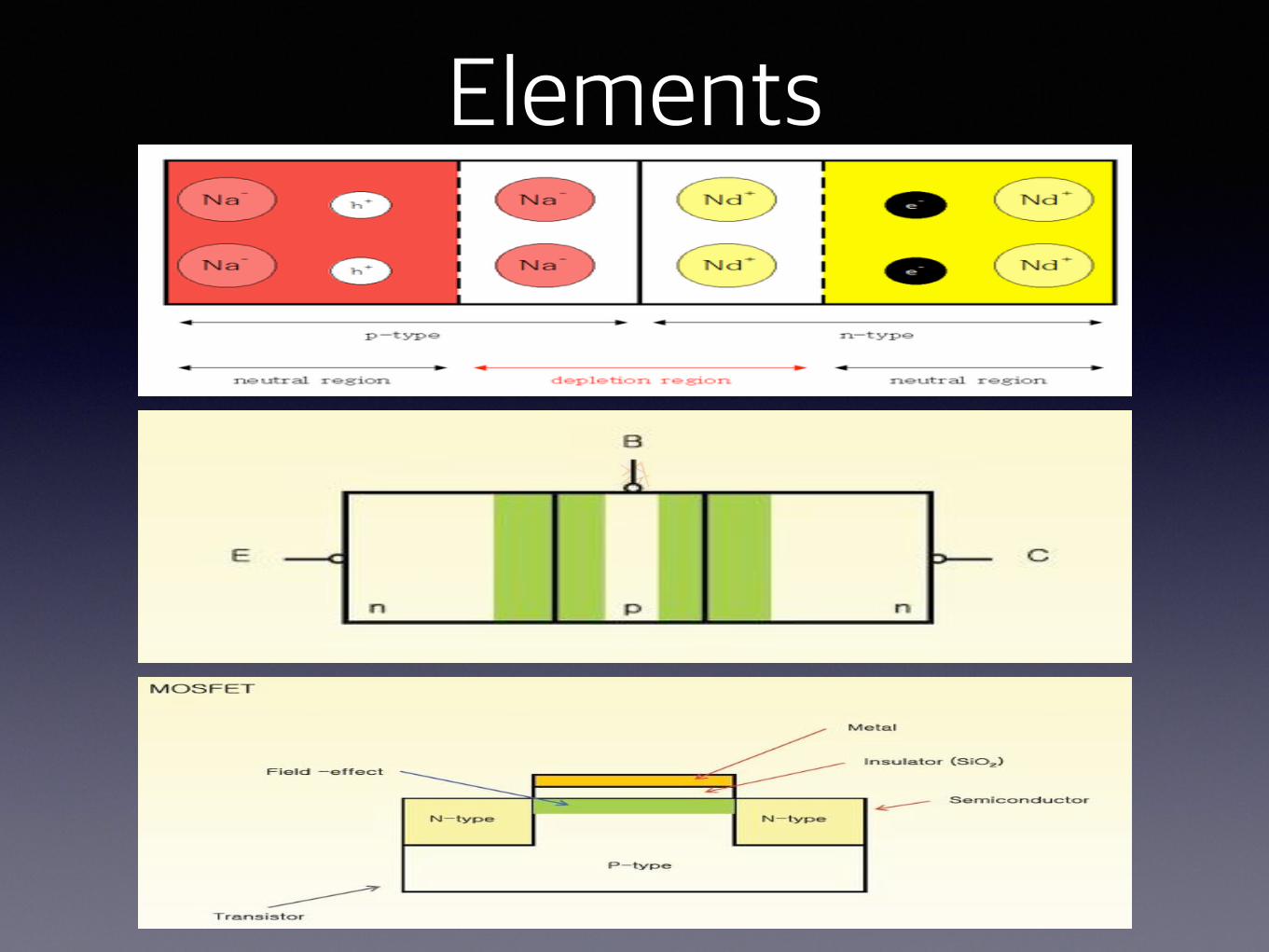
Elements• Diode, Transistor
• By putting N-type and P-type Semiconductor together, they form a Diode( )
• When 3 semiconductors are put together in forms of NPN or PNP, they form a Transistor (Bipolar Junction Transistor)
• MOSFET (Metal Oxide Semiconductor Field Effect Transistor) has a different structure
P d N
Elements
Elements
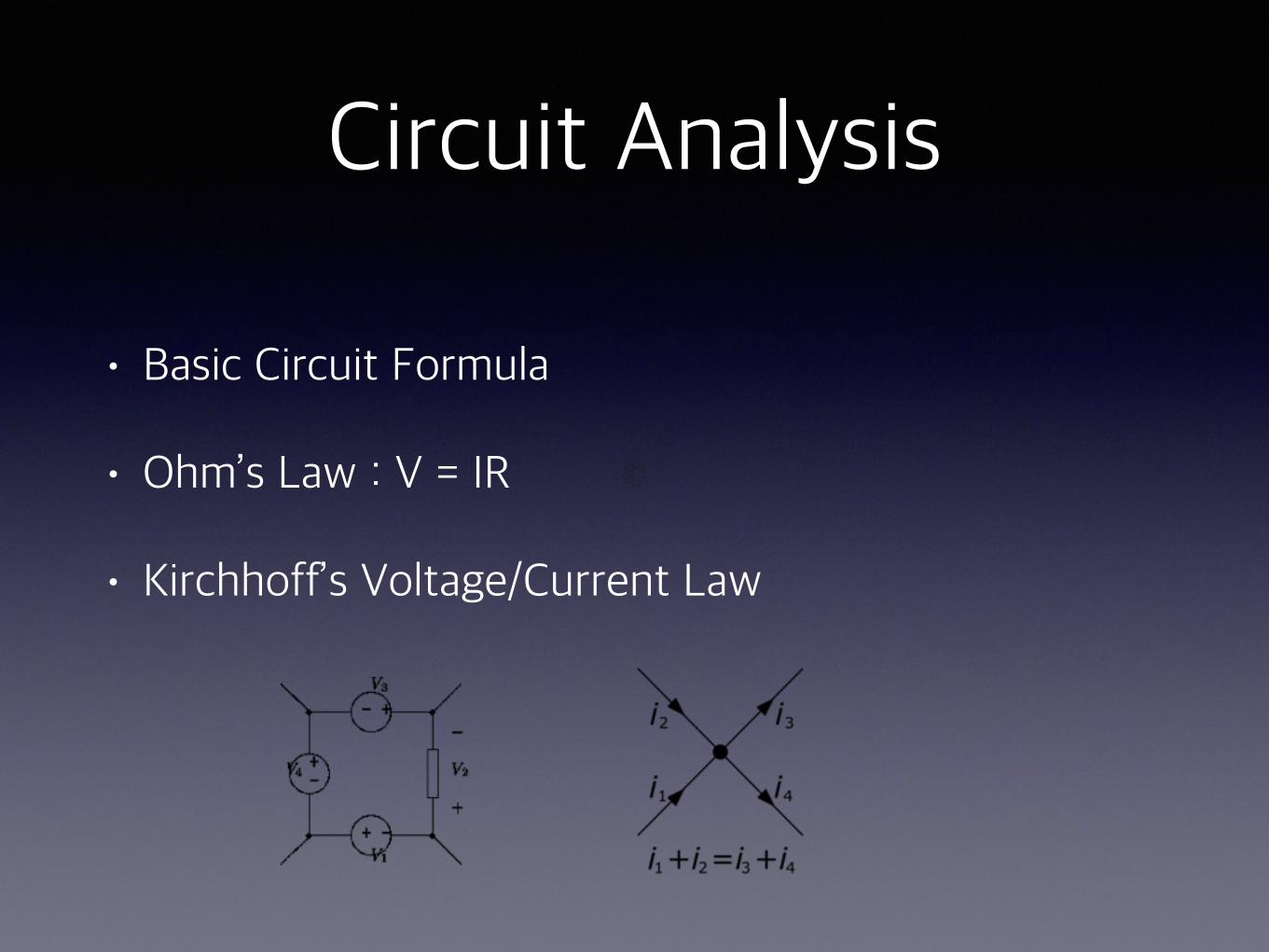
Circuit Analysis
• Basic Circuit Formula
• Ohm’s Law : V = IR
• Kirchhoff’s Voltage/Current Law
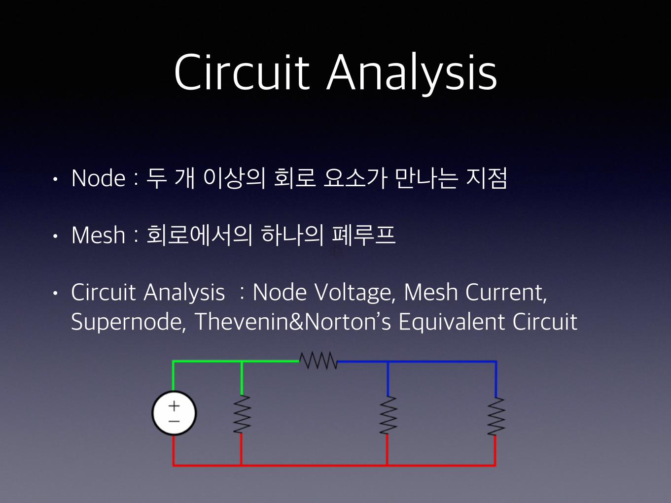
Circuit Analysis
• Node : 두 개 이상의 회로 요소가 만나는 지점
• Mesh : 회로에서의 하나의 폐루프
• Circuit Analysis : Node Voltage, Mesh Current, Supernode, Thevenin&Norton’s Equivalent Circuit
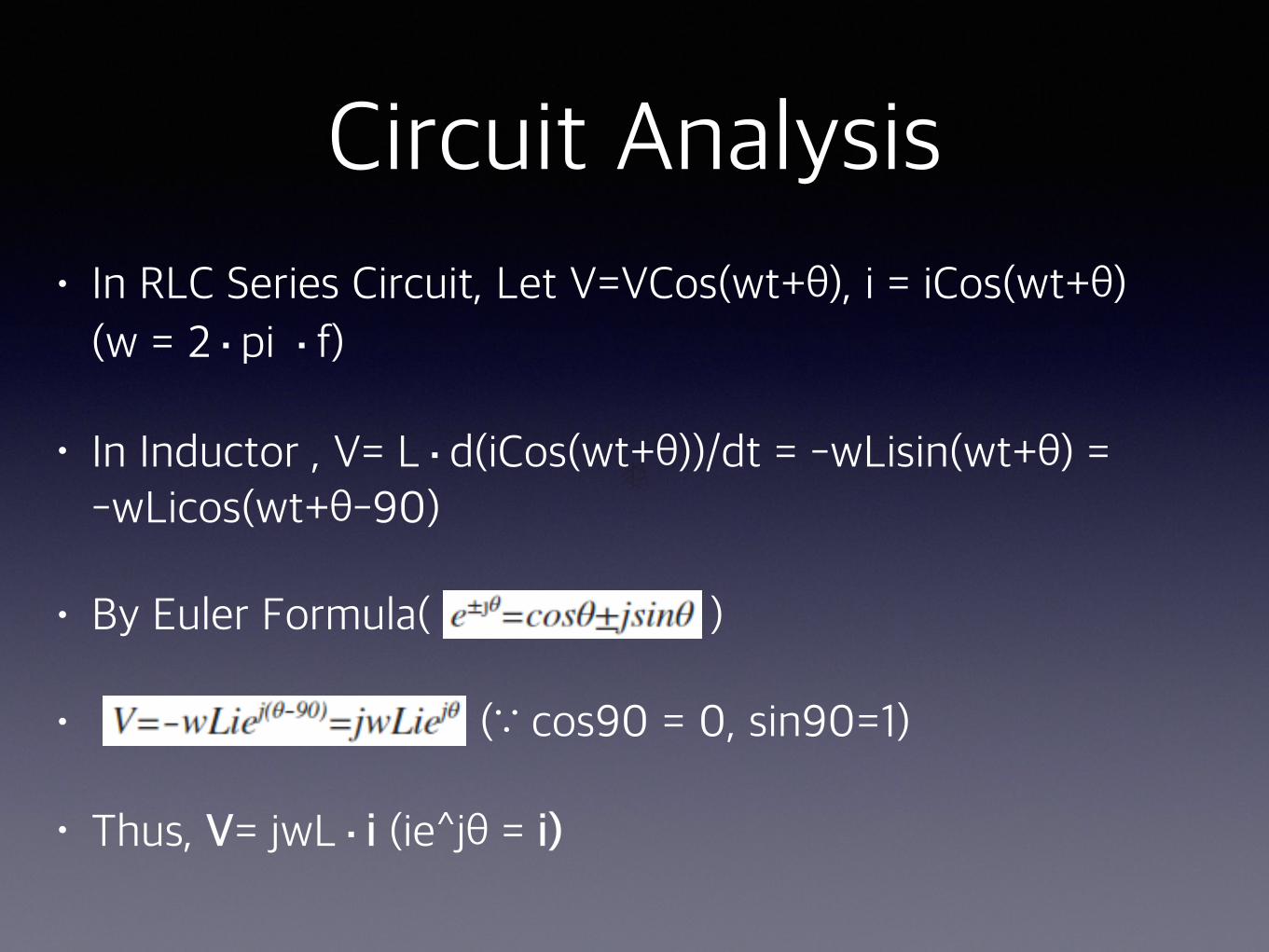
Circuit Analysis• In RLC Series Circuit, Let V=VCos(wt+θ), i = iCos(wt+θ)
(w = 2·pi ·f)
• In Inductor , V= L·d(iCos(wt+θ))/dt = -wLisin(wt+θ) = -wLicos(wt+θ-90)
• By Euler Formula( )
• (∵ cos90 = 0, sin90=1)
• Thus, V= jwL·i (ie^jθ = i)
Circuit Analysis
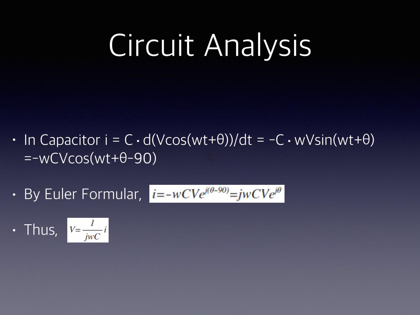
• In Capacitor i = C·d(Vcos(wt+θ))/dt = -C·wVsin(wt+θ) =-wCVcos(wt+θ-90)
• By Euler Formular,
• Thus,
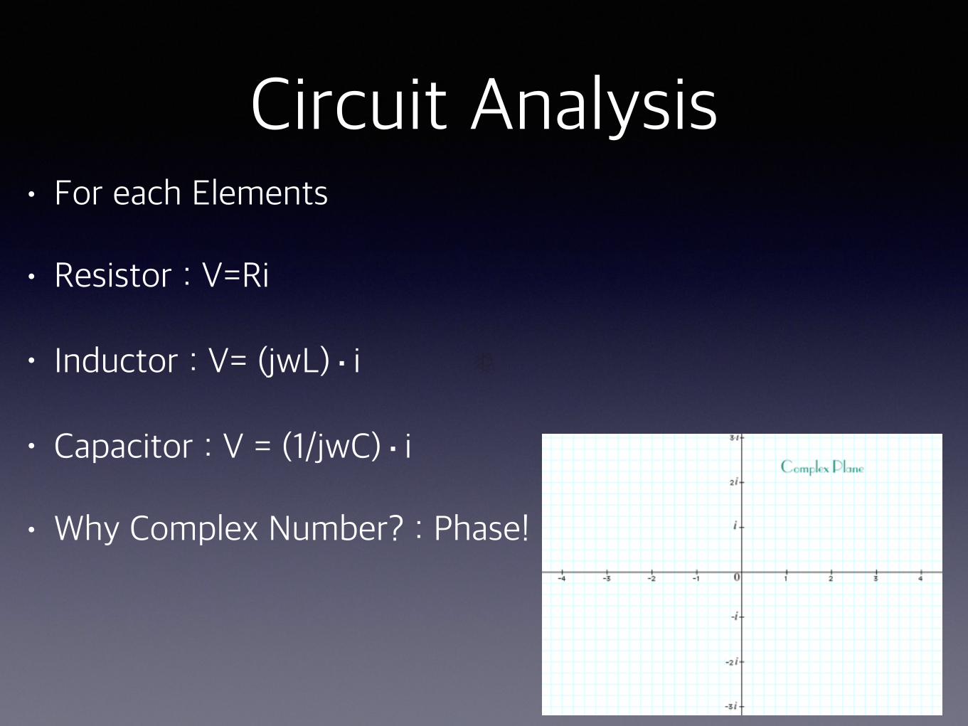
Circuit Analysis• For each Elements
• Resistor : V=Ri
• Inductor : V= (jwL)·i
• Capacitor : V = (1/jwC)·i
• Why Complex Number? : Phase!
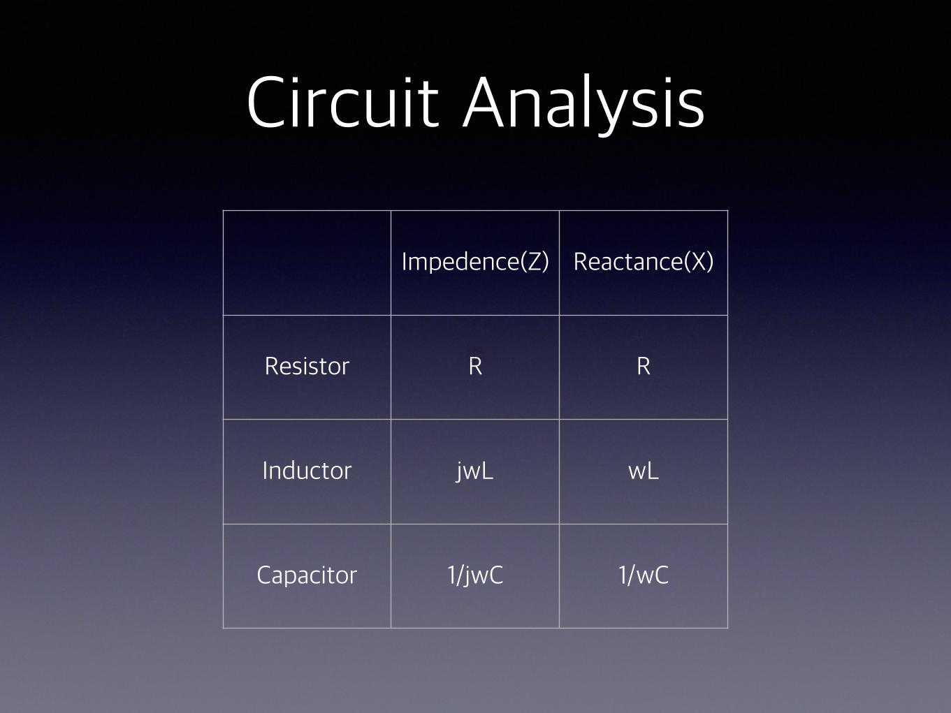
Circuit Analysis
Impedence(Z) Reactance(X)
Resistor R R
Inductor jwL wL
Capacitor 1/jwC 1/wC
Circuit Analysis
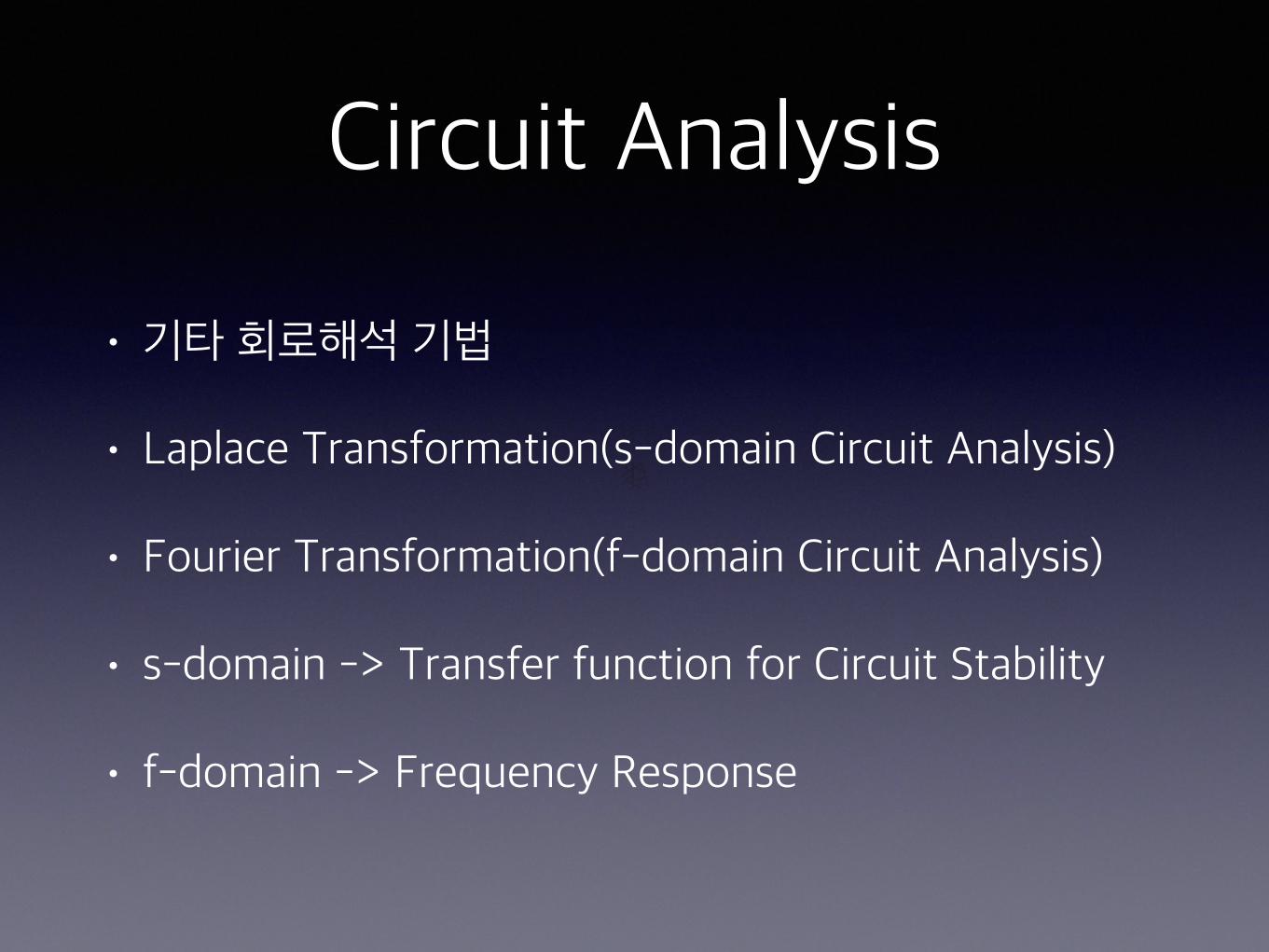
• 기타 회로해석 기법
• Laplace Transformation(s-domain Circuit Analysis)
• Fourier Transformation(f-domain Circuit Analysis)
• s-domain -> Transfer function for Circuit Stability
• f-domain -> Frequency Response
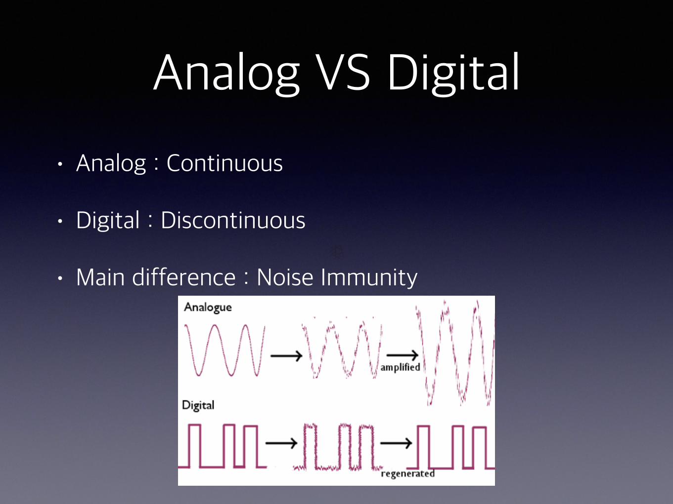
Analog VS Digital
• Analog : Continuous
• Digital : Discontinuous
• Main difference : Noise Immunity
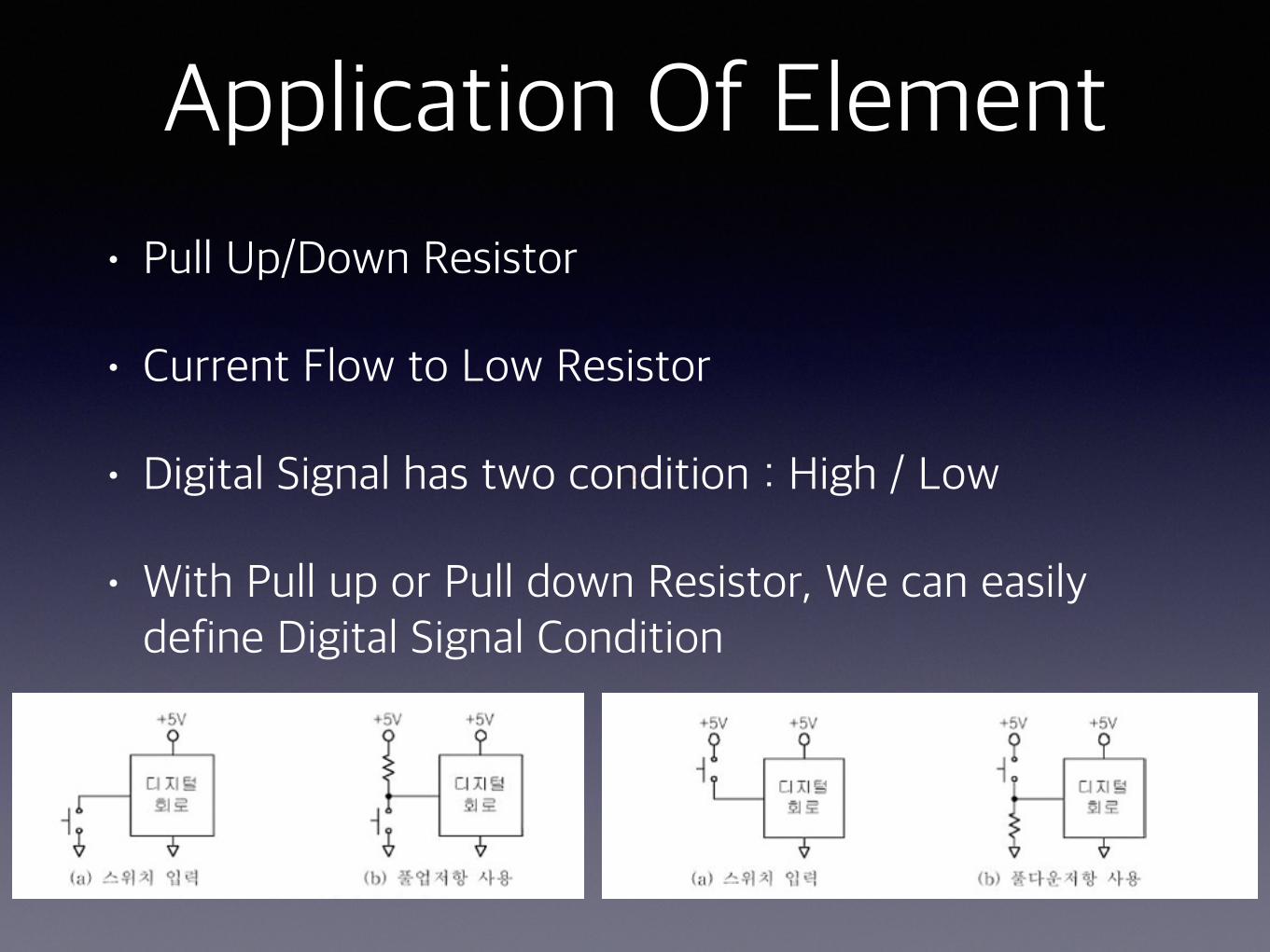
Application Of Element
• Pull Up/Down Resistor
• Current Flow to Low Resistor
• Digital Signal has two condition : High / Low
• With Pull up or Pull down Resistor, We can easily define Digital Signal Condition
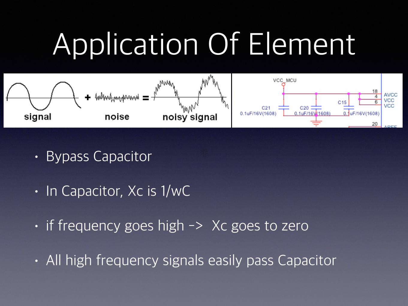
Application Of Element
• Bypass Capacitor
• In Capacitor, Xc is 1/wC
• if frequency goes high -> Xc goes to zero
• All high frequency signals easily pass Capacitor
Application of Element• Bead(Not Inductor, But Very Similar)
• Digital Signal has a very high frequency when compared to Analog Signal
• In Inductor, Reactance is wL
• High frequency cannot pass Inductor(Reactance goes to infinity)
• Easily Separate Analog and Digital Signal
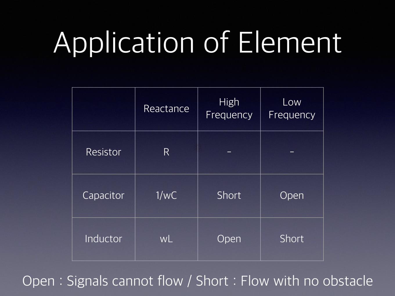
Application of Element
ReactanceHigh
FrequencyLow
Frequency
Resistor R - -
Capacitor 1/wC Short Open
Inductor wL Open Short
Open : Signals cannot flow / Short : Flow with no obstacle
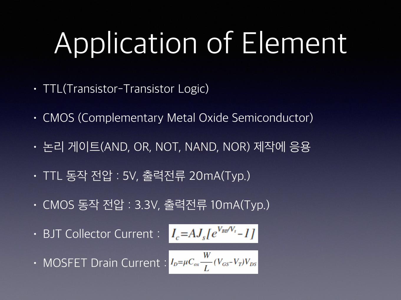
Application of Element• TTL(Transistor-Transistor Logic)
• CMOS (Complementary Metal Oxide Semiconductor)
• 논리 게이트(AND, OR, NOT, NAND, NOR) 제작에 응용
• TTL 동작 전압 : 5V, 출력전류 20mA(Typ.)
• CMOS 동작 전압 : 3.3V, 출력전류 10mA(Typ.)
• BJT Collector Current :
• MOSFET Drain Current :
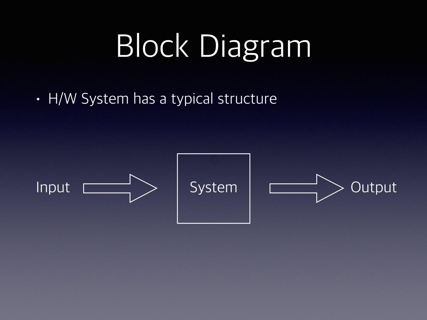
Block Diagram
• H/W System has a typical structure
Input OutputSystem
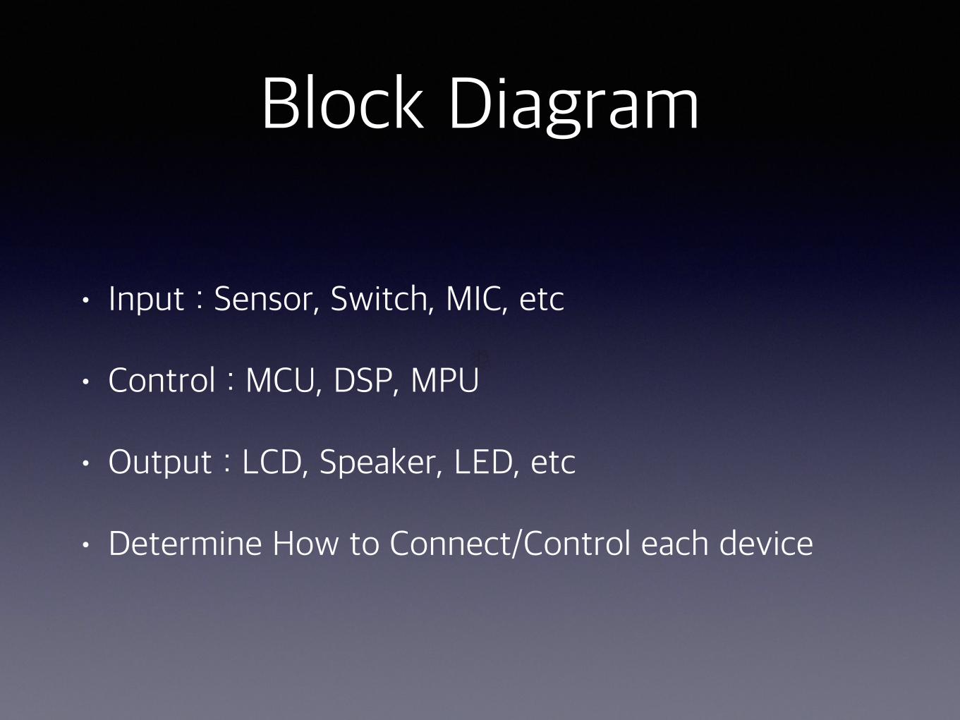
Block Diagram
• Input : Sensor, Switch, MIC, etc
• Control : MCU, DSP, MPU
• Output : LCD, Speaker, LED, etc
• Determine How to Connect/Control each device
Design H/W System
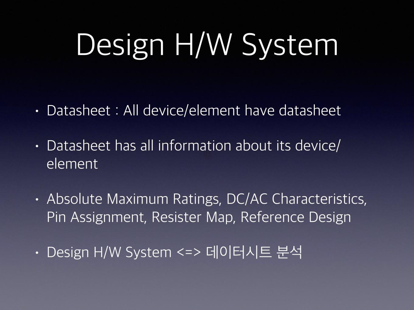
• Datasheet : All device/element have datasheet
• Datasheet has all information about its device/element
• Absolute Maximum Ratings, DC/AC Characteristics, Pin Assignment, Resister Map, Reference Design
• Design H/W System <=> 데이터시트 분석
이 세미나는 다음과 같이 진행되었습니다 우선적으로 하드웨어 개발에 있어서 가장 필수적인 회로 소자들을 소개하고 그 소자(Element)가 어떤 역할을 하는지에 대해 설명했습
니다. 그 후 회로를 통과하는 신호를 두 가지로 나누어서 설명하고 두 신호의 제어에 있어서 위에 설명한 소자들이 이 신호제어에 있어서 어떻
게 응용이 되는지 실무와 연관해서 설명하였습니다 최종적으로 이 이론들을 가지고 하드웨어를 설계/개발함에 있어서 추가적으로 필요한 부분들을 소개하고 실제적으로 제가 개발하는 제
품에 어떻게 응용했는지를 설명을 했습니다 그 예를 제가 개발중인 Wand로 설명했는데, 회사 개발자분들과의 세미나다 보니 모든 소스와 설계도를 오픈했지만, 블로그에 올리기
에는 적합하지 않다 생각하여 아예 삭제하였습니다