Applications • Switching applications STF11N65M5, … · N-channel 650 V, 0.43 Ω typ., 9 A...
30
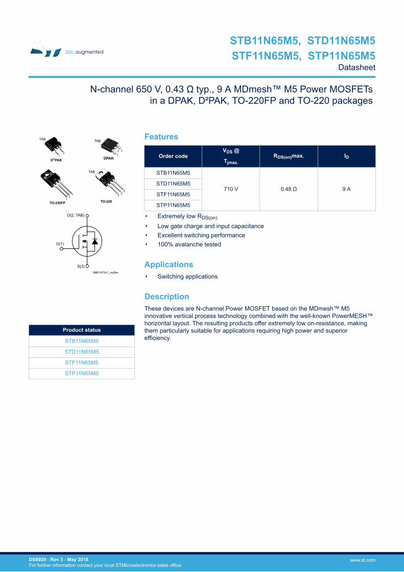
1 2 3 TO-220 TAB 1 2 3 TO-220FP 1 3 TAB D PAK 2 DPAK 1 3 2 TAB AM01475v1_noZen D(2, TAB) G(1) S(3) Features Order code V DS @ T jmax. R DS(on) max. I D STB11N65M5 710 V 0.48 Ω 9 A STD11N65M5 STF11N65M5 STP11N65M5 • Extremely low R DS(on) • Low gate charge and input capacitance • Excellent switching performance • 100% avalanche tested Applications • Switching applications Description These devices are N-channel Power MOSFET based on the MDmesh™ M5 innovative vertical process technology combined with the well-known PowerMESH™ horizontal layout. The resulting products offer extremely low on-resistance, making them particularly suitable for applications requiring high power and superior efficiency. Product status STB11N65M5 STD11N65M5 STF11N65M5 STP11N65M5 N-channel 650 V, 0.43 Ω typ., 9 A MDmesh™ M5 Power MOSFETs in a DPAK, D²PAK, TO-220FP and TO-220 packages STB11N65M5, STD11N65M5 STF11N65M5, STP11N65M5 Datasheet DS8920 - Rev 3 - May 2018 For further information contact your local STMicroelectronics sales office. www.st.com
Transcript of Applications • Switching applications STF11N65M5, … · N-channel 650 V, 0.43 Ω typ., 9 A...
1 23
TO-220
TAB
12
3
TO-220FP
13
TAB
D PAK2 DPAK1
32
TAB
AM01475v1_noZen
D(2, TAB)
G(1)
S(3)
Features
Order codeVDS @
Tjmax.RDS(on)max. ID
STB11N65M5
710 V 0.48 Ω 9 ASTD11N65M5
STF11N65M5
STP11N65M5
• Extremely low RDS(on)
• Low gate charge and input capacitance• Excellent switching performance• 100% avalanche tested
Applications• Switching applications
DescriptionThese devices are N-channel Power MOSFET based on the MDmesh™ M5innovative vertical process technology combined with the well-known PowerMESH™horizontal layout. The resulting products offer extremely low on-resistance, makingthem particularly suitable for applications requiring high power and superiorefficiency.
Product status
STB11N65M5
STD11N65M5
STF11N65M5
STP11N65M5
N-channel 650 V, 0.43 Ω typ., 9 A MDmesh™ M5 Power MOSFETs in a DPAK, D²PAK, TO-220FP and TO-220 packages
STB11N65M5, STD11N65M5 STF11N65M5, STP11N65M5
Datasheet
DS8920 - Rev 3 - May 2018For further information contact your local STMicroelectronics sales office.
www.st.com
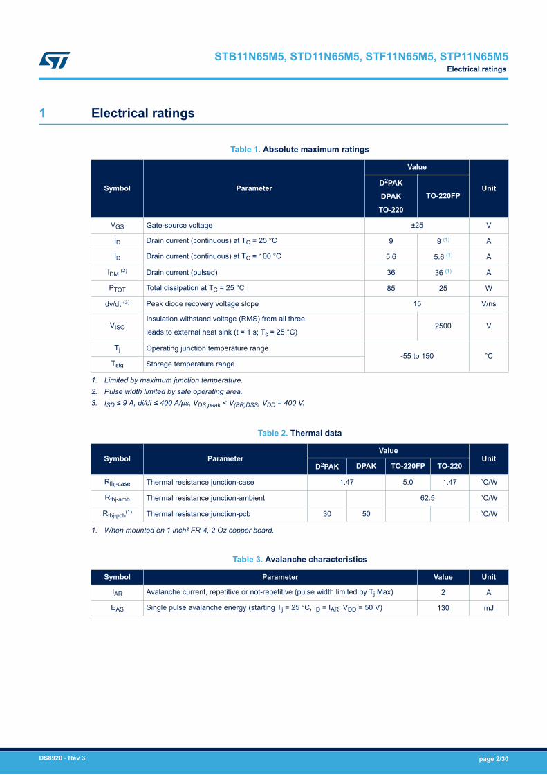
1 Electrical ratings
Table 1. Absolute maximum ratings
Symbol Parameter
Value
UnitD2PAK
DPAK
TO-220
TO-220FP
VGS Gate-source voltage ±25 V
ID Drain current (continuous) at TC = 25 °C 9 9 (1) A
ID Drain current (continuous) at TC = 100 °C 5.6 5.6 (1) A
IDM (2) Drain current (pulsed) 36 36 (1) A
PTOT Total dissipation at TC = 25 °C 85 25 W
dv/dt (3) Peak diode recovery voltage slope 15 V/ns
VISOInsulation withstand voltage (RMS) from all three
leads to external heat sink (t = 1 s; Tc = 25 °C)2500 V
Tj Operating junction temperature range-55 to 150 °C
Tstg Storage temperature range
1. Limited by maximum junction temperature.2. Pulse width limited by safe operating area.3. ISD ≤ 9 A, di/dt ≤ 400 A/μs; VDS peak < V(BR)DSS, VDD = 400 V.
Table 2. Thermal data
Symbol ParameterValue
UnitD2PAK DPAK TO-220FP TO-220
Rthj-case Thermal resistance junction-case 1.47 5.0 1.47 °C/W
Rthj-amb Thermal resistance junction-ambient 62.5 °C/W
Rthj-pcb(1) Thermal resistance junction-pcb 30 50 °C/W
1. When mounted on 1 inch² FR-4, 2 Oz copper board.
Table 3. Avalanche characteristics
Symbol Parameter Value Unit
IAR Avalanche current, repetitive or not-repetitive (pulse width limited by Tj Max) 2 A
EAS Single pulse avalanche energy (starting Tj = 25 °C, ID = IAR, VDD = 50 V) 130 mJ
STB11N65M5, STD11N65M5, STF11N65M5, STP11N65M5Electrical ratings
DS8920 - Rev 3 page 2/30
2 Electrical characteristics
(TCASE = 25 °C unless otherwise specified)
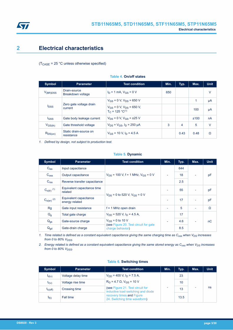
Table 4. On/off states
Symbol Parameter Test condition Min. Typ. Max. Unit
V(BR)DSSDrain-sourceBreakdown voltage ID = 1 mA, VGS = 0 V 650 V
IDSSZero gate voltage draincurrent
VGS = 0 V, VDS = 650 V 1 µA
VGS = 0 V, VDS = 650 V,TC = 125 °C(1) 100 µA
IGSS Gate body leakage current VDS = 0 V, VGS = ±25 V ±100 nA
VGS(th) Gate threshold voltage VDS = VGS, ID = 250 µA 3 4 5 V
RDS(on)Static drain-source onresistance VGS = 10 V, ID = 4.5 A 0.43 0.48 Ω
1. Defined by design, not subject to production test.
Table 5. Dynamic
Symbol Parameter Test condition Min. Typ. Max. Unit
Ciss Input capacitance
VDS = 100 V, f = 1 MHz, VGS = 0 V -
644
- pFCoss Output capacitance 18
Crss Reverse transfer capacitance 2.5
Co(tr) (1) Equivalent capacitance timerelated
VDS = 0 to 520 V, VGS = 0 V- 55 - pF
Co(er) (2) Equivalent capacitanceenergy related - 17 - pF
Rg Gate input resistance f = 1 MHz open drain - 5 - Ω
Qg Total gate charge VDD = 520 V, ID = 4.5 A,
VGS = 0 to 10 V(see Figure 20. Test circuit for gatecharge behavior)
-
17
- nCQgs Gate-source charge 4.6
Qgd Gate-drain charge 8.5
1. Time related is defined as a constant equivalent capacitance giving the same charging time as Coss when VDS increasesfrom 0 to 80% VDSS.
2. Energy related is defined as a constant equivalent capacitance giving the same stored energy as Coss when VDS increasesfrom 0 to 80% VDSS.
Table 6. Switching times
Symbol Parameter Test condition Min. Typ. Max. Unit
td(v) Voltage delay time VDD = 400 V, ID = 7.5 A,
RG = 4.7 Ω, VGS = 10 V
(see Figure 21. Test circuit forinductive load switching and dioderecovery times and Figure24. Switching time waveform)
-
23
- nstr(v) Voltage rise time 10
tc(off) Crossing time 13
tf(i) Fall time 13.5
STB11N65M5, STD11N65M5, STF11N65M5, STP11N65M5Electrical characteristics
DS8920 - Rev 3 page 3/30
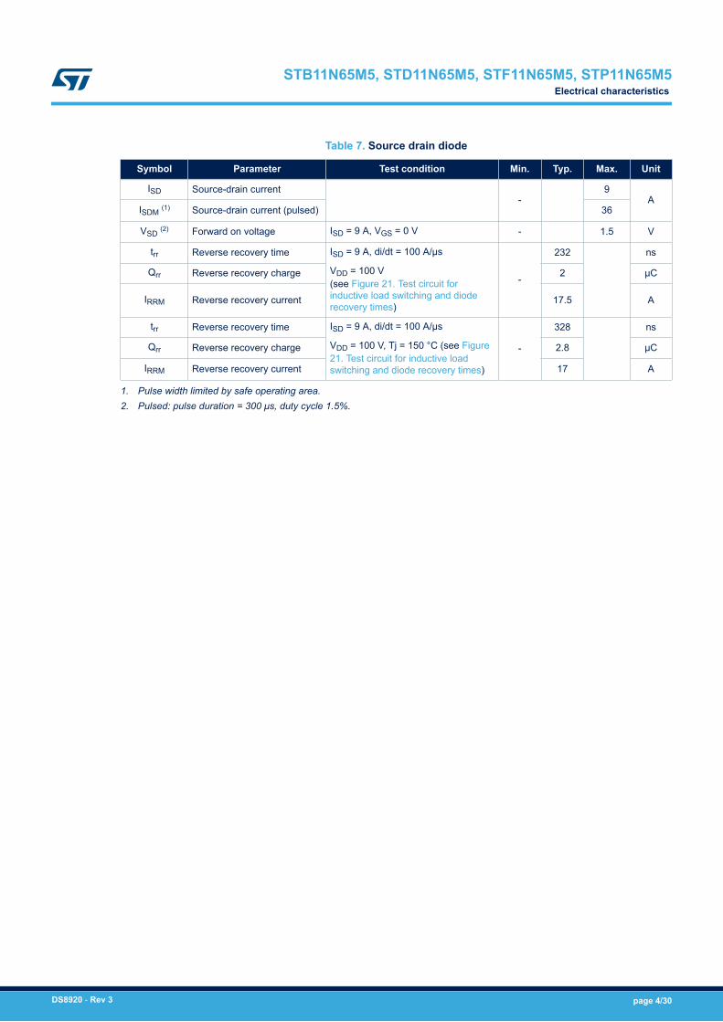
Table 7. Source drain diode
Symbol Parameter Test condition Min. Typ. Max. Unit
ISD Source-drain current-
9A
ISDM (1) Source-drain current (pulsed) 36
VSD (2) Forward on voltage ISD = 9 A, VGS = 0 V - 1.5 V
trr Reverse recovery time ISD = 9 A, di/dt = 100 A/µs
VDD = 100 V(see Figure 21. Test circuit forinductive load switching and dioderecovery times)
-
232 ns
Qrr Reverse recovery charge 2 μC
IRRM Reverse recovery current 17.5 A
trr Reverse recovery time ISD = 9 A, di/dt = 100 A/µs
VDD = 100 V, Tj = 150 °C (see Figure21. Test circuit for inductive loadswitching and diode recovery times)
-
328 ns
Qrr Reverse recovery charge 2.8 μC
IRRM Reverse recovery current 17 A
1. Pulse width limited by safe operating area.2. Pulsed: pulse duration = 300 μs, duty cycle 1.5%.
STB11N65M5, STD11N65M5, STF11N65M5, STP11N65M5Electrical characteristics
DS8920 - Rev 3 page 4/30
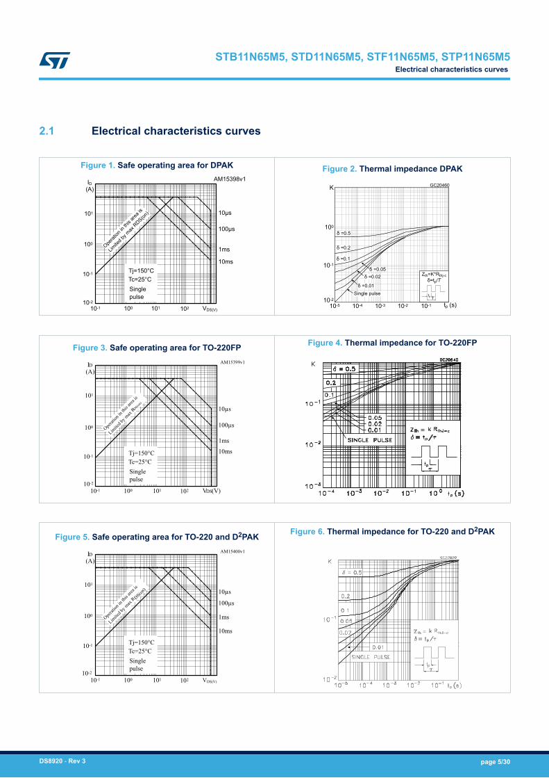
2.1 Electrical characteristics curves
Figure 1. Safe operating area for DPAK
ID
101
100
10-1
10-1 100 VDS(V)101
(A)
Operat
ion in
this
area i
s
Limite
d by m
ax R
DS(on)
10ms
10µs
Tj=150°CTc=25°CSinglepulse
1ms
102
100µs
AM15398v1
10-2
Figure 2. Thermal impedance DPAK
GC20460
100
10-1
10-2
10-5 10-4 10-3 10-2 10-1
K
tp (s)
Figure 3. Safe operating area for TO-220FP
ID
101
100
10-1
10-1 100 VDS(V)101
(A)
Operati
on in
this a
rea is
Limite
d by m
ax RDS(on
)
10ms
10µs
Tj=150°CTc=25°CSinglepulse
1ms
10-2
102
100µs
AM15399v1
Figure 4. Thermal impedance for TO-220FP
Figure 5. Safe operating area for TO-220 and D2PAK
ID
101
100
10-1
10-1 100 VDS(V)101
(A)
Operati
on in
this a
rea is
Limite
d by m
ax R DS(on
)
10ms
10µs
Tj=150°CTc=25°CSinglepulse
1ms
10-2
102
100µs
AM15400v1
Figure 6. Thermal impedance for TO-220 and D2PAK
STB11N65M5, STD11N65M5, STF11N65M5, STP11N65M5Electrical characteristics curves
DS8920 - Rev 3 page 5/30
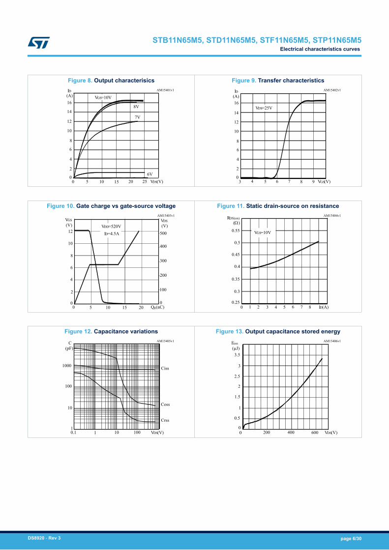
Figure 8. Output characterisicsID
6
4
2
00 5 VDS(V)15
(A)
10
8
6V
7V
VGS=10V
20
8V
25
16
14
12
10
AM15401v1
Figure 9. Transfer characteristicsID
8
6
2
03 6 VGS(V)
(A)
4
4
5
VDS=25V
7 8 9
10
12
14
16
AM15402v1
Figure 10. Gate charge vs gate-source voltage
VGS
6
4
2
00 5 Qg(nC)
(V)
8
10 15
10
VDD=520VID=4.5A
20
12
300
200
100
0
400
500
VDS(V)
AM15403v1
Figure 11. Static drain-source on resistance
RDS(on)
0.4
0.35
0.3
0.250 2 ID(A)
(W)
1
0.45
0.5
VGS=10V
3 4 5 6 7 8
0.55
AM15404v1
Figure 12. Capacitance variations
C
100
10.1 1 VDS(V)
(pF)
10
Ciss
Coss
Crss
10
100
1000
AM15405v1
Figure 13. Output capacitance stored energy
Eoss
1
0.5
00 VDS(V)
(µJ)
400
1.5
200
2
2.5
600
3
3.5
AM15406v1
STB11N65M5, STD11N65M5, STF11N65M5, STP11N65M5Electrical characteristics curves
DS8920 - Rev 3 page 6/30
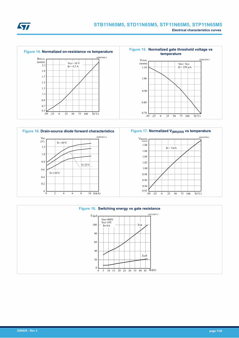
Figure 14. Normalized on-resistance vs temperature
RDS(on)
1.7
1.3
0.9
0.5-50 0 TJ(°C)
(norm)
-25 7525 50 100
0.7
1.1
1.5
1.9
2.1 ID = 4.5 AVGS = 10 V
AM05460v1
Figure 15. Normalized gate threshold voltage vstemperature
VGS(th)
1.00
0.90
0.80
0.70-50 0 TJ(°C)
(norm)
-25
1.10
7525 50 100
ID = 250 µAVDS = VGS
AM05459v1
Figure 16. Drain-source diode forward characteristics
VSD
0 4 ISD(A)
(V)
2 106 80
0.2
0.4
0.6
0.8
1.0
1.2TJ=-50°C
TJ=150°C
TJ=25°C
AM05461v1
Figure 17. Normalized V(BR)DSS vs temperature
V(BR)DSS
-50 0 TJ(°C)
(norm)
-25 7525 50 1000.920.94
0.96
0.98
1.00
1.04
1.06
1.02
ID = 1mA1.08
AM10399v1
Figure 18. Switching energy vs gate resistance
E
00 20 RG(W)
(µJ)
10 30
20
40
40
ID=6A
VDD=400V
Eon
Eoff
60
VGS=10V
80
100
5 15 25 35 45
AM15407v1
STB11N65M5, STD11N65M5, STF11N65M5, STP11N65M5Electrical characteristics curves
DS8920 - Rev 3 page 7/30
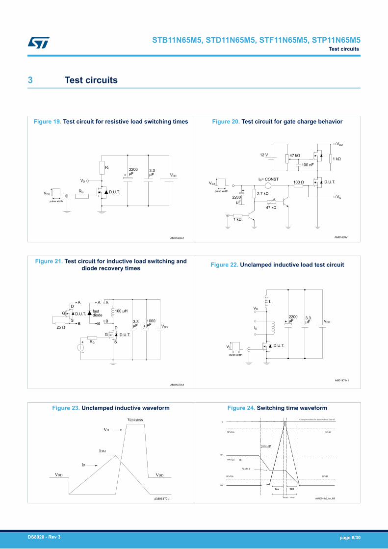
3 Test circuits
Figure 19. Test circuit for resistive load switching times
AM01468v1
VD
RG
RL
D.U.T.
2200μF VDD
3.3μF+
pulse width
VGS
Figure 20. Test circuit for gate charge behavior
AM01469v1
47 kΩ1 kΩ
47 kΩ
2.7 kΩ
1 kΩ
12 V
IG= CONST100 Ω
100 nF
D.U.T.
+pulse width
VGS
2200μF
VG
VDD
Figure 21. Test circuit for inductive load switching anddiode recovery times
AM01470v1
AD
D.U.T.S
B
G
25 Ω
A A
B B
RG
GD
S
100 µH
µF3.3 1000
µF VDD
D.U.T.
+
_
+
fastdiode
Figure 22. Unclamped inductive load test circuit
AM01471v1
VD
ID
D.U.T.
L
VDD+
pulse width
Vi
3.3µF
2200µF
Figure 23. Unclamped inductive waveform
AM01472v1
V(BR)DSS
VDDVDD
VD
IDM
ID
Figure 24. Switching time waveform
AM05540v2_for_M5
Id
Vgs
Vds
90%Vds
10%Id
90%Vgs on
Tdelay -off
TfallTrise
Tcross -over
10%Vds
90%Id
Vgs(I(t ))
on
-off
TfallTrise
-
))
Concept waveform for Inductive Load Turn-off
STB11N65M5, STD11N65M5, STF11N65M5, STP11N65M5Test circuits
DS8920 - Rev 3 page 8/30
4 Package information
In order to meet environmental requirements, ST offers these devices in different grades of ECOPACK®
packages, depending on their level of environmental compliance. ECOPACK® specifications, grade definitionsand product status are available at: www.st.com. ECOPACK® is an ST trademark.
STB11N65M5, STD11N65M5, STF11N65M5, STP11N65M5Package information
DS8920 - Rev 3 page 9/30
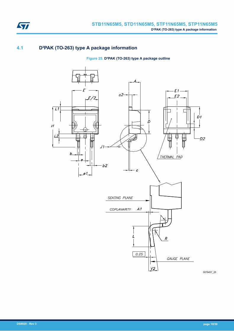
4.1 D²PAK (TO-263) type A package information
Figure 25. D²PAK (TO-263) type A package outline
0079457_25
STB11N65M5, STD11N65M5, STF11N65M5, STP11N65M5D²PAK (TO-263) type A package information
DS8920 - Rev 3 page 10/30
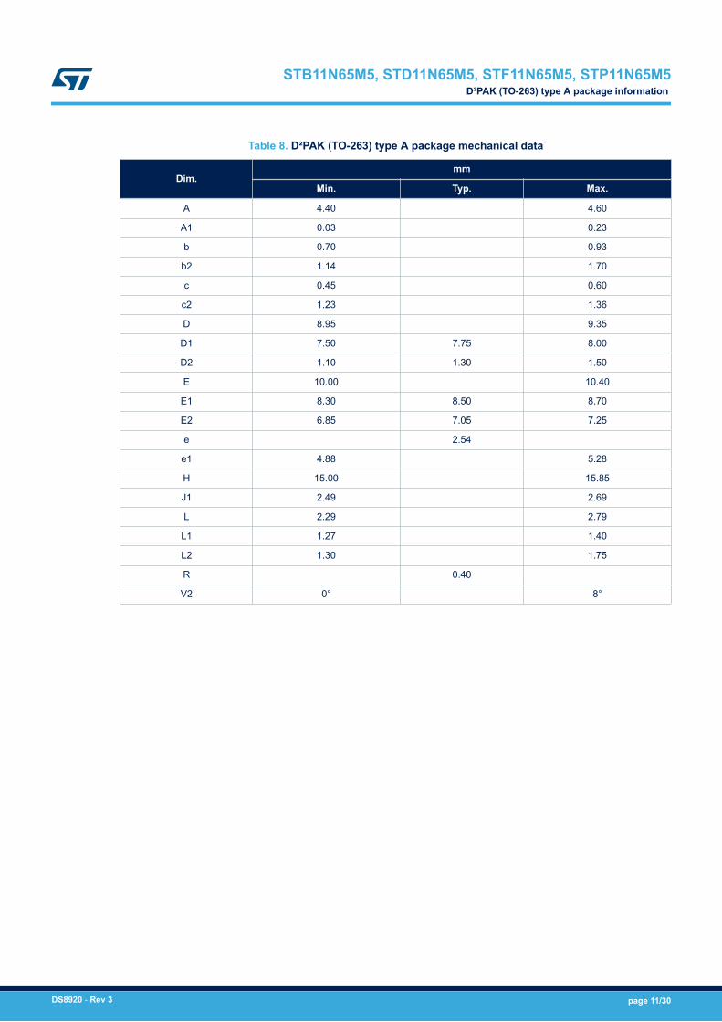
Table 8. D²PAK (TO-263) type A package mechanical data
Dim.mm
Min. Typ. Max.
A 4.40 4.60
A1 0.03 0.23
b 0.70 0.93
b2 1.14 1.70
c 0.45 0.60
c2 1.23 1.36
D 8.95 9.35
D1 7.50 7.75 8.00
D2 1.10 1.30 1.50
E 10.00 10.40
E1 8.30 8.50 8.70
E2 6.85 7.05 7.25
e 2.54
e1 4.88 5.28
H 15.00 15.85
J1 2.49 2.69
L 2.29 2.79
L1 1.27 1.40
L2 1.30 1.75
R 0.40
V2 0° 8°
STB11N65M5, STD11N65M5, STF11N65M5, STP11N65M5D²PAK (TO-263) type A package information
DS8920 - Rev 3 page 11/30
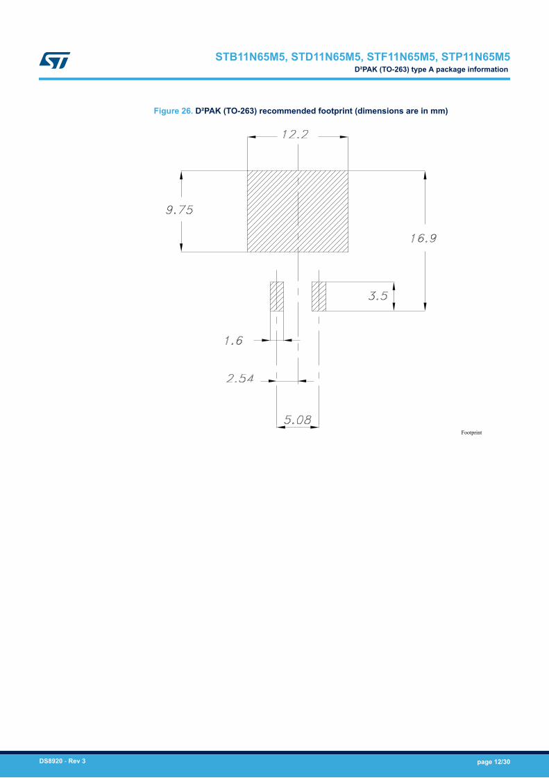
Figure 26. D²PAK (TO-263) recommended footprint (dimensions are in mm)
Footprint
STB11N65M5, STD11N65M5, STF11N65M5, STP11N65M5D²PAK (TO-263) type A package information
DS8920 - Rev 3 page 12/30
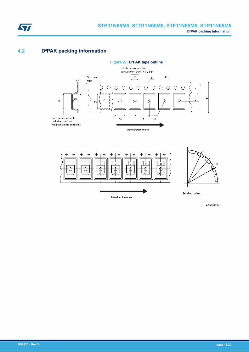
4.2 D²PAK packing information
Figure 27. D²PAK tape outline
STB11N65M5, STD11N65M5, STF11N65M5, STP11N65M5D²PAK packing information
DS8920 - Rev 3 page 13/30
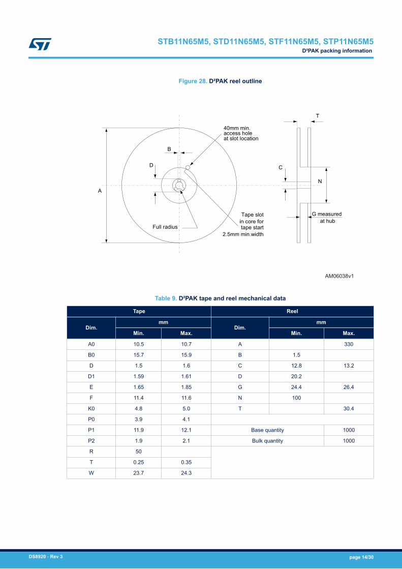
Figure 28. D²PAK reel outline
A
D
B
Full radius
Tape slot in core for tape start
2.5mm min.width
G measured at hub
C
N
40mm min. access hole at slot location
T
AM06038v1
Table 9. D²PAK tape and reel mechanical data
Tape Reel
Dim.mm
Dim.mm
Min. Max. Min. Max.
A0 10.5 10.7 A 330
B0 15.7 15.9 B 1.5
D 1.5 1.6 C 12.8 13.2
D1 1.59 1.61 D 20.2
E 1.65 1.85 G 24.4 26.4
F 11.4 11.6 N 100
K0 4.8 5.0 T 30.4
P0 3.9 4.1
P1 11.9 12.1 Base quantity 1000
P2 1.9 2.1 Bulk quantity 1000
R 50
T 0.25 0.35
W 23.7 24.3
STB11N65M5, STD11N65M5, STF11N65M5, STP11N65M5D²PAK packing information
DS8920 - Rev 3 page 14/30
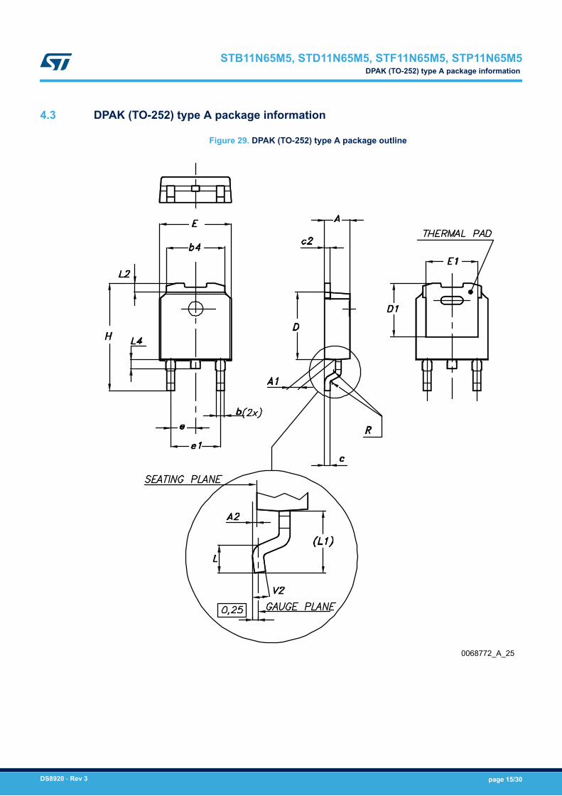
4.3 DPAK (TO-252) type A package information
Figure 29. DPAK (TO-252) type A package outline
0068772_A_25
STB11N65M5, STD11N65M5, STF11N65M5, STP11N65M5DPAK (TO-252) type A package information
DS8920 - Rev 3 page 15/30

Table 10. DPAK (TO-252) type A mechanical data
Dim.mm
Min. Typ. Max.
A 2.20 2.40
A1 0.90 1.10
A2 0.03 0.23
b 0.64 0.90
b4 5.20 5.40
c 0.45 0.60
c2 0.48 0.60
D 6.00 6.20
D1 4.95 5.10 5.25
E 6.40 6.60
E1 4.60 4.70 4.80
e 2.159 2.286 2.413
e1 4.445 4.572 4.699
H 9.35 10.10
L 1.00 1.50
(L1) 2.60 2.80 3.00
L2 0.65 0.80 0.95
L4 0.60 1.00
R 0.20
V2 0° 8°
STB11N65M5, STD11N65M5, STF11N65M5, STP11N65M5DPAK (TO-252) type A package information
DS8920 - Rev 3 page 16/30
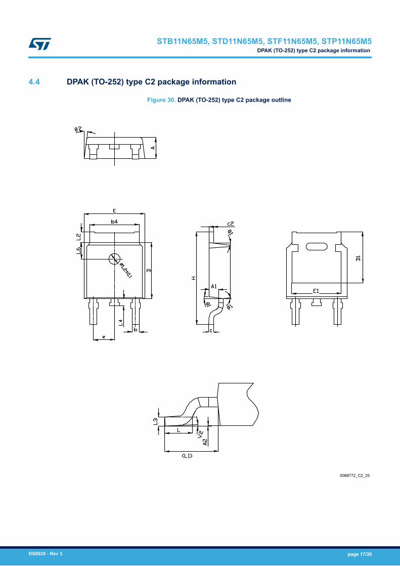
4.4 DPAK (TO-252) type C2 package information
Figure 30. DPAK (TO-252) type C2 package outline
0068772_C2_25
STB11N65M5, STD11N65M5, STF11N65M5, STP11N65M5DPAK (TO-252) type C2 package information
DS8920 - Rev 3 page 17/30
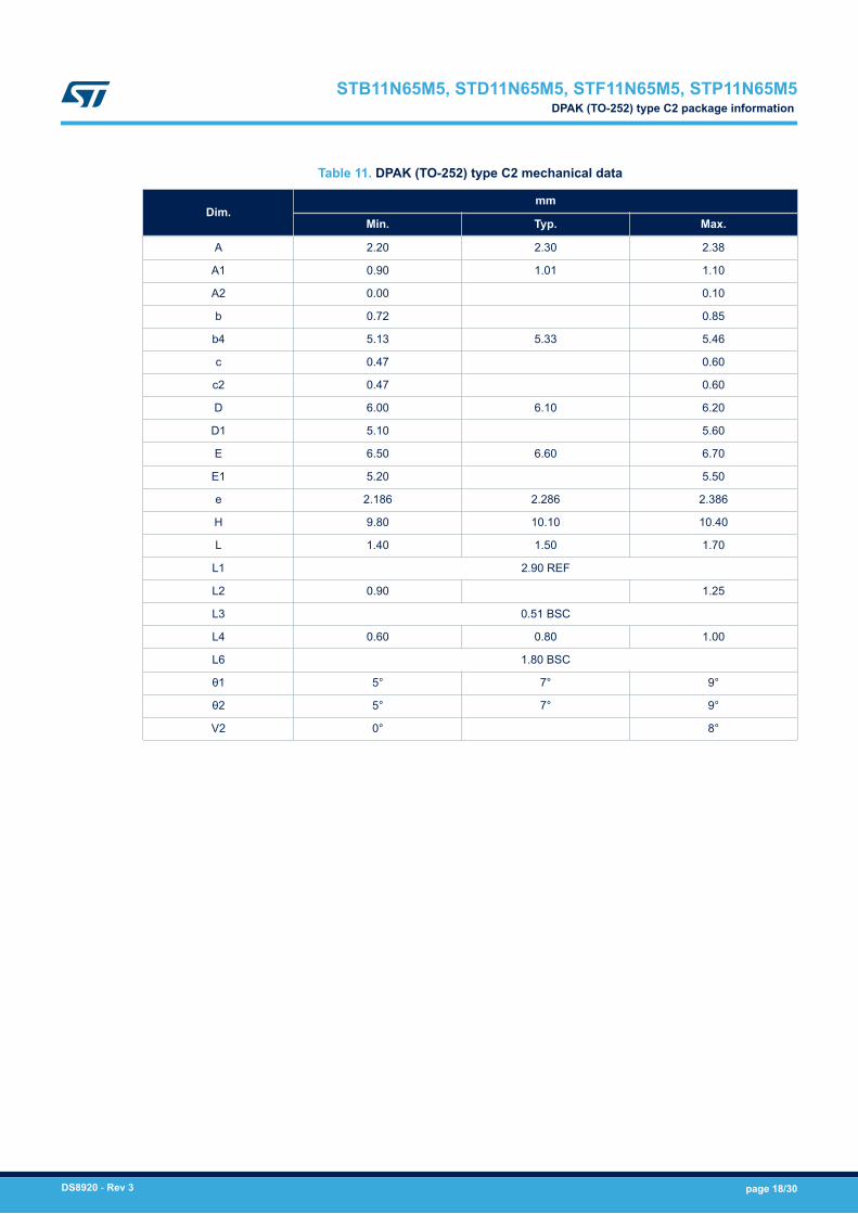
Table 11. DPAK (TO-252) type C2 mechanical data
Dim.mm
Min. Typ. Max.
A 2.20 2.30 2.38
A1 0.90 1.01 1.10
A2 0.00 0.10
b 0.72 0.85
b4 5.13 5.33 5.46
c 0.47 0.60
c2 0.47 0.60
D 6.00 6.10 6.20
D1 5.10 5.60
E 6.50 6.60 6.70
E1 5.20 5.50
e 2.186 2.286 2.386
H 9.80 10.10 10.40
L 1.40 1.50 1.70
L1 2.90 REF
L2 0.90 1.25
L3 0.51 BSC
L4 0.60 0.80 1.00
L6 1.80 BSC
θ1 5° 7° 9°
θ2 5° 7° 9°
V2 0° 8°
STB11N65M5, STD11N65M5, STF11N65M5, STP11N65M5DPAK (TO-252) type C2 package information
DS8920 - Rev 3 page 18/30
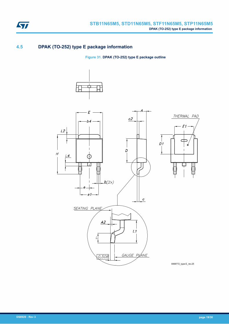
4.5 DPAK (TO-252) type E package information
Figure 31. DPAK (TO-252) type E package outline
0068772_type-E_rev.25
STB11N65M5, STD11N65M5, STF11N65M5, STP11N65M5DPAK (TO-252) type E package information
DS8920 - Rev 3 page 19/30
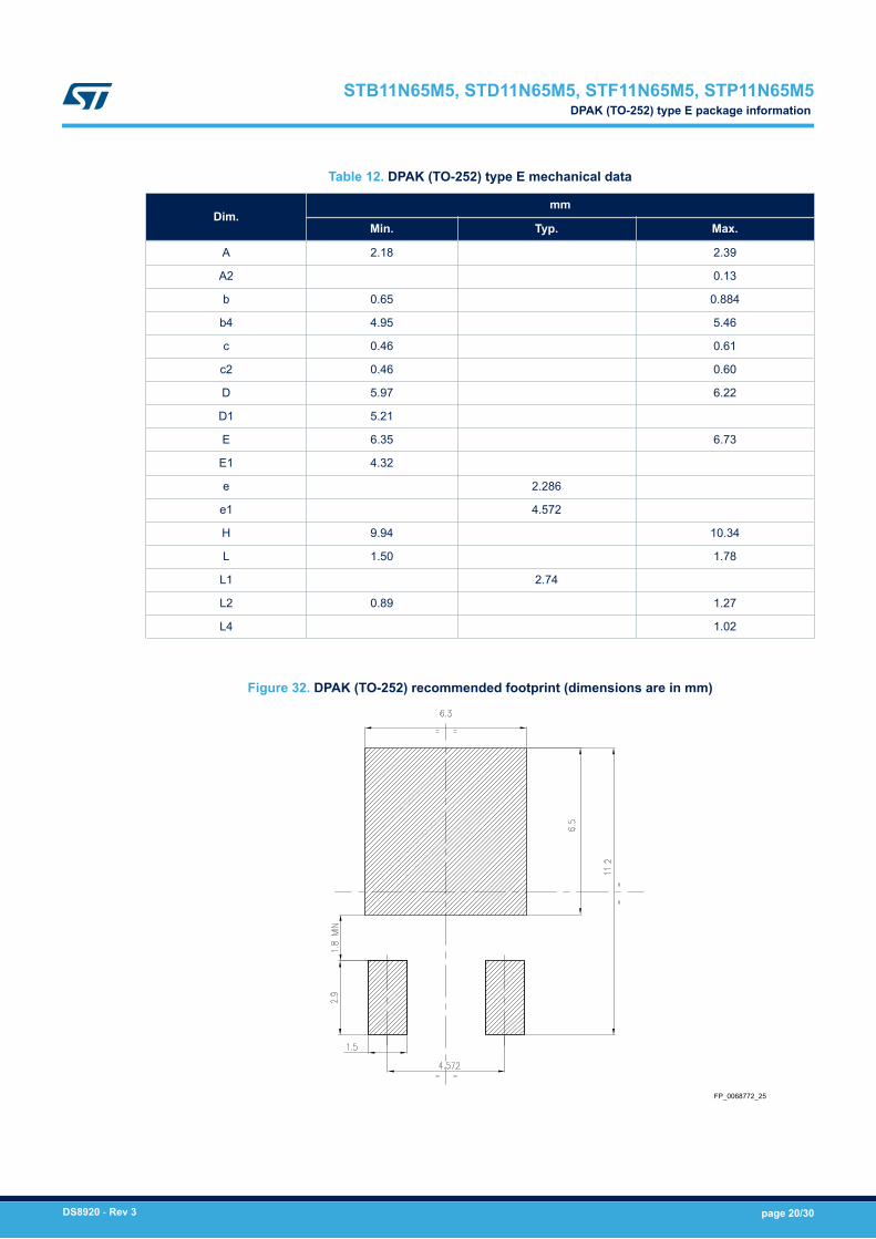
Table 12. DPAK (TO-252) type E mechanical data
Dim.mm
Min. Typ. Max.
A 2.18 2.39
A2 0.13
b 0.65 0.884
b4 4.95 5.46
c 0.46 0.61
c2 0.46 0.60
D 5.97 6.22
D1 5.21
E 6.35 6.73
E1 4.32
e 2.286
e1 4.572
H 9.94 10.34
L 1.50 1.78
L1 2.74
L2 0.89 1.27
L4 1.02
Figure 32. DPAK (TO-252) recommended footprint (dimensions are in mm)
FP_0068772_25
STB11N65M5, STD11N65M5, STF11N65M5, STP11N65M5DPAK (TO-252) type E package information
DS8920 - Rev 3 page 20/30
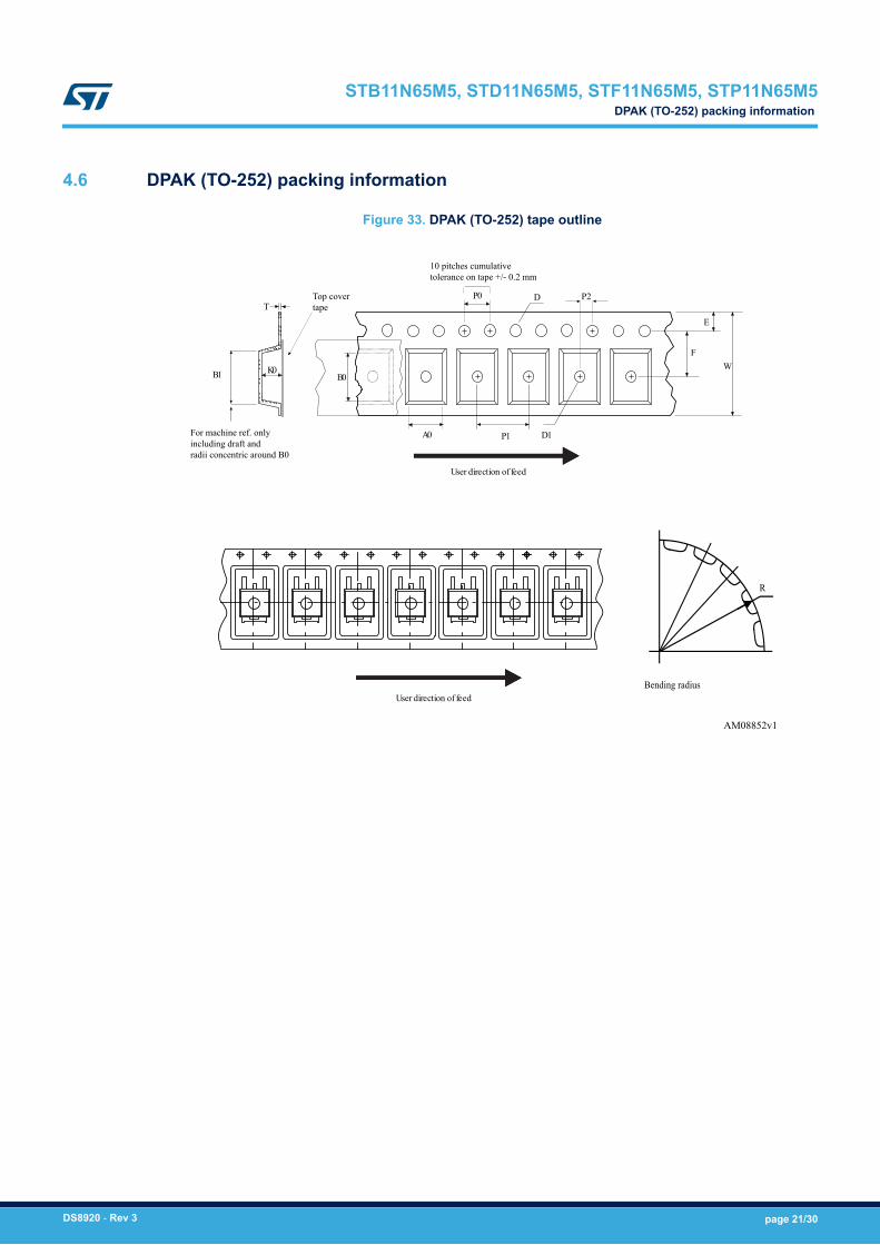
4.6 DPAK (TO-252) packing information
Figure 33. DPAK (TO-252) tape outline
P1A0 D1
P0
FW
E
D
B0K0
T
User direction of feed
P2
10 pitches cumulativetolerance on tape +/- 0.2 mm
User direction of feed
R
Bending radius
B1
For machine ref. onlyincluding draft andradii concentric around B0
AM08852v1
Top covertape
STB11N65M5, STD11N65M5, STF11N65M5, STP11N65M5DPAK (TO-252) packing information
DS8920 - Rev 3 page 21/30

Figure 34. DPAK (TO-252) reel outline
A
D
B
Full radius
Tape slot in core for tape start
2.5mm min.width
G measured at hub
C
N
40mm min. access hole at slot location
T
AM06038v1
Table 13. DPAK (TO-252) tape and reel mechanical data
Tape Reel
Dim.mm
Dim.mm
Min. Max. Min. Max.
A0 6.8 7 A 330
B0 10.4 10.6 B 1.5
B1 12.1 C 12.8 13.2
D 1.5 1.6 D 20.2
D1 1.5 G 16.4 18.4
E 1.65 1.85 N 50
F 7.4 7.6 T 22.4
K0 2.55 2.75
P0 3.9 4.1 Base qty. 2500
P1 7.9 8.1 Bulk qty. 2500
P2 1.9 2.1
R 40
T 0.25 0.35
W 15.7 16.3
STB11N65M5, STD11N65M5, STF11N65M5, STP11N65M5DPAK (TO-252) packing information
DS8920 - Rev 3 page 22/30
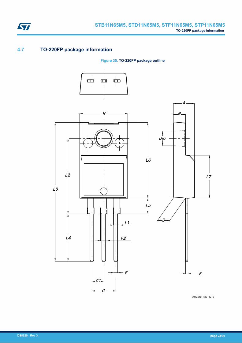
4.7 TO-220FP package information
Figure 35. TO-220FP package outline
7012510_Rev_12_B
STB11N65M5, STD11N65M5, STF11N65M5, STP11N65M5TO-220FP package information
DS8920 - Rev 3 page 23/30

Table 14. TO-220FP package mechanical data
Dim.mm
Min. Typ. Max.
A 4.4 4.6
B 2.5 2.7
D 2.5 2.75
E 0.45 0.7
F 0.75 1
F1 1.15 1.70
F2 1.15 1.70
G 4.95 5.2
G1 2.4 2.7
H 10 10.4
L2 16
L3 28.6 30.6
L4 9.8 10.6
L5 2.9 3.6
L6 15.9 16.4
L7 9 9.3
Dia 3 3.2
STB11N65M5, STD11N65M5, STF11N65M5, STP11N65M5TO-220FP package information
DS8920 - Rev 3 page 24/30
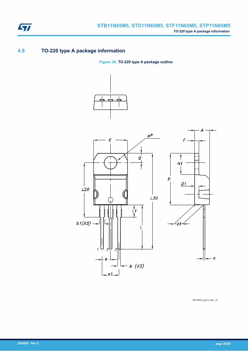
4.8 TO-220 type A package information
Figure 36. TO-220 type A package outline
0015988_typeA_Rev_21
STB11N65M5, STD11N65M5, STF11N65M5, STP11N65M5TO-220 type A package information
DS8920 - Rev 3 page 25/30
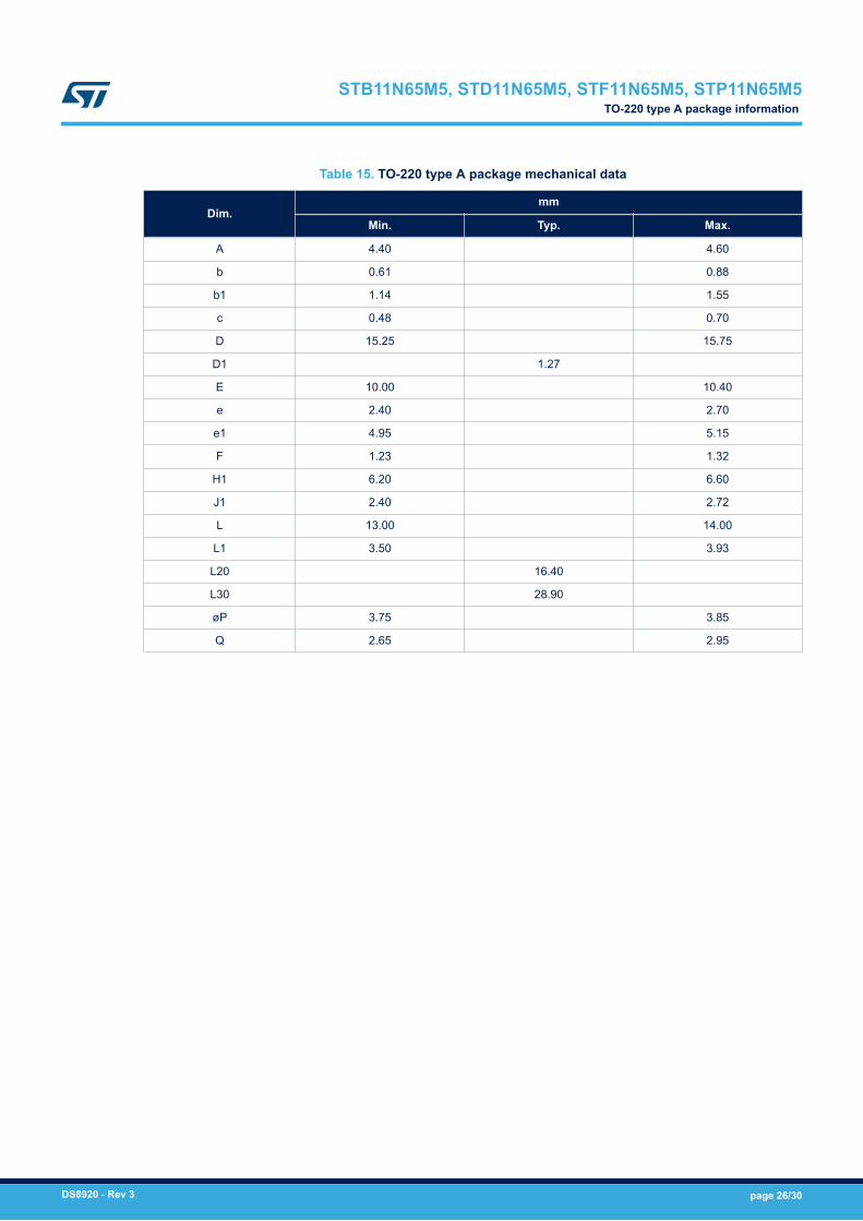
Table 15. TO-220 type A package mechanical data
Dim.mm
Min. Typ. Max.
A 4.40 4.60
b 0.61 0.88
b1 1.14 1.55
c 0.48 0.70
D 15.25 15.75
D1 1.27
E 10.00 10.40
e 2.40 2.70
e1 4.95 5.15
F 1.23 1.32
H1 6.20 6.60
J1 2.40 2.72
L 13.00 14.00
L1 3.50 3.93
L20 16.40
L30 28.90
øP 3.75 3.85
Q 2.65 2.95
STB11N65M5, STD11N65M5, STF11N65M5, STP11N65M5TO-220 type A package information
DS8920 - Rev 3 page 26/30
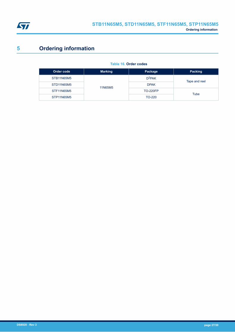
5 Ordering information
Table 16. Order codes
Order code Marking Package Packing
STB11N65M5
11N65M5
D2PAKTape and reel
STD11N65M5 DPAK
STF11N65M5 TO-220FPTube
STP11N65M5 TO-220
STB11N65M5, STD11N65M5, STF11N65M5, STP11N65M5Ordering information
DS8920 - Rev 3 page 27/30
Revision history
Table 17. Document revision history
Date Version Changes
23-Feb-2012 1 First release.
03-Dec-2012 2
– Minor text changes in cover page
– Added IPAK packages
– Added Section 2.1: Electrical characteristics (curves)
– Updated Section 5: Packaging mechanical data
– Modified: note 2 on Table 2
– Updated: mechanical data for TO-220FP package
02-May-2018 3
The part number STU11N65M5 has been moved to a separate datasheet.
Removed maturity status indication from cover page. The document status isproduction data.
Updated title and features in cover page, Section 1 Electrical ratings, Section2 Electrical characteristics, Section 2.1 Electrical characteristics curves andSection 4 Package information.
Minor text changes.
STB11N65M5, STD11N65M5, STF11N65M5, STP11N65M5
DS8920 - Rev 3 page 28/30
Contents
1 Electrical ratings . . . . . . . . . . . . . . . . . . . . . . . . . . . . . . . . . . . . . . . . . . . . . . . . . . . . . . . . . . . . . . . . . .2
2 Electrical characteristics. . . . . . . . . . . . . . . . . . . . . . . . . . . . . . . . . . . . . . . . . . . . . . . . . . . . . . . . . . .3
2.1 Electrical characteristics curves . . . . . . . . . . . . . . . . . . . . . . . . . . . . . . . . . . . . . . . . . . . . . . . . . . 5
3 Test circuits . . . . . . . . . . . . . . . . . . . . . . . . . . . . . . . . . . . . . . . . . . . . . . . . . . . . . . . . . . . . . . . . . . . . . . .8
4 Package information. . . . . . . . . . . . . . . . . . . . . . . . . . . . . . . . . . . . . . . . . . . . . . . . . . . . . . . . . . . . . . .9
4.1 D²PAK (TO-263) type A package information . . . . . . . . . . . . . . . . . . . . . . . . . . . . . . . . . . . . . . . 9
4.2 D²PAK packing information . . . . . . . . . . . . . . . . . . . . . . . . . . . . . . . . . . . . . . . . . . . . . . . . . . . . . 12
4.3 DPAK (TO-252) type A package information . . . . . . . . . . . . . . . . . . . . . . . . . . . . . . . . . . . . . . . 14
4.4 DPAK (TO-252) type C2 package information . . . . . . . . . . . . . . . . . . . . . . . . . . . . . . . . . . . . . . 16
4.5 DPAK (TO-252) type E package information . . . . . . . . . . . . . . . . . . . . . . . . . . . . . . . . . . . . . . . 18
4.6 DPAK (TO-252) packing information. . . . . . . . . . . . . . . . . . . . . . . . . . . . . . . . . . . . . . . . . . . . . . 20
4.7 TO-220FP package information . . . . . . . . . . . . . . . . . . . . . . . . . . . . . . . . . . . . . . . . . . . . . . . . . 22
4.8 TO-220 type A package information . . . . . . . . . . . . . . . . . . . . . . . . . . . . . . . . . . . . . . . . . . . . . . 24
5 Ordering information . . . . . . . . . . . . . . . . . . . . . . . . . . . . . . . . . . . . . . . . . . . . . . . . . . . . . . . . . . . . .27
Revision history . . . . . . . . . . . . . . . . . . . . . . . . . . . . . . . . . . . . . . . . . . . . . . . . . . . . . . . . . . . . . . . . . . . . . . .28
STB11N65M5, STD11N65M5, STF11N65M5, STP11N65M5Contents
DS8920 - Rev 3 page 29/30
IMPORTANT NOTICE – PLEASE READ CAREFULLY
STMicroelectronics NV and its subsidiaries (“ST”) reserve the right to make changes, corrections, enhancements, modifications, and improvements to STproducts and/or to this document at any time without notice. Purchasers should obtain the latest relevant information on ST products before placing orders. STproducts are sold pursuant to ST’s terms and conditions of sale in place at the time of order acknowledgement.
Purchasers are solely responsible for the choice, selection, and use of ST products and ST assumes no liability for application assistance or the design ofPurchasers’ products.
No license, express or implied, to any intellectual property right is granted by ST herein.
Resale of ST products with provisions different from the information set forth herein shall void any warranty granted by ST for such product.
ST and the ST logo are trademarks of ST. All other product or service names are the property of their respective owners.
Information in this document supersedes and replaces information previously supplied in any prior versions of this document.
© 2018 STMicroelectronics – All rights reserved
STB11N65M5, STD11N65M5, STF11N65M5, STP11N65M5
DS8920 - Rev 3 page 30/30