![[TI] SINGLE P-CHANNEL ENHANCEMENT-MODE MOSFETS.PDF](https://static.fdocument.org/doc/165x107/55cf8ec3550346703b95588a/ti-single-p-channel-enhancement-mode-mosfetspdf.jpg)
Advanced AD/DA converters Overview Digital Enhancement ...
9
Digital Enhancement Techniques Pietro Andreani Dept. of Electrical and Information Technology Lund University, Sweden Advanced AD/DA converters Advanced AD/DA converters Digital Enhancement Techniques 2 Overview • Single-bit vs. multi-bit modulator • Dual quantization • Dynamic element matching (DEM) • Digital correction Advanced AD/DA converters Digital Enhancement Techniques 3 Single-bit vs. multi-bit 2 DD ref swing V V α β < High SNR with single-bit ΔΣ high-order modulators (however, stability issues) and/or high OSR High OSR, and bandwidth of the op-amps that must be higher than clock frequency ok for audio or instrumentation applications (in general, for “low frequency” applications) Usable V ref with single-bit is a small fraction of the supply voltage, since the swing at the op-amp outputs is rather large – assume that the dynamic range at the op-amp output is , and that a -6dB FS input gives rise to a swing of at the output of the first integrator the maximum V ref is then given by For low supply voltages, α may be only 0.7, and DD V α swing ref V β ± ,6 2 swing dBFS β − = 0.175 ref DD V V = This and next 2 slides from Maloberti’s book Advanced AD/DA converters Digital Enhancement Techniques 4 Single-bit vs. multi-bit – II Such a low value of V ref is problematic, because of the constraints on the kT/C noise (if DT modulator) and op-amp thermal noise (γkT/C L ), especially for the first op-amp 1-bit quantization is easier with medium-high supply voltages Slew-rate issue input of first integrator is the difference between analog input and DAC output; the DAC output follows the input with an accuracy dependent on the DAC resolution (and input bandwidth) reasonable to assume that the maximum difference is 2Δ if 1-bit, this becomes 2V ref either very high SR, or low V ref with multi-bit, integrator input is reduced by the number of quantization levels Multi-bit additional power in ADC On the other hand, the resolution of a modulator can be increased by increasing the OSR optimal use of power entails a trade-off between increased speed in op-amps (if higher OSR) and more comparators in quantizer (if more quantizer bits)
Transcript of Advanced AD/DA converters Overview Digital Enhancement ...
Digital Enhancement Techniques
Pietro AndreaniDept. of Electrical and Information Technology
Lund University, Sweden
Advanced AD/DA converters
Advanced AD/DA converters Digital Enhancement Techniques 2
Overview
• Single-bit vs. multi-bit modulator
• Dual quantization
• Dynamic element matching (DEM)
• Digital correction
Advanced AD/DA converters Digital Enhancement Techniques 3
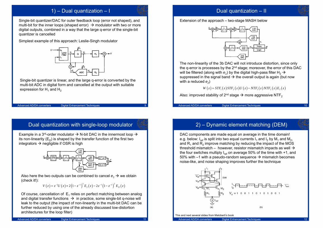
Single-bit vs. multi-bit
2DD
refswing
VV αβ
<
High SNR with single-bit ΔΣ high-order modulators (however, stability issues) and/or high OSR
High OSR, and bandwidth of the op-amps that must be higher than clock frequency ok for audio or instrumentation applications (in general, for “low frequency” applications)
Usable Vref with single-bit is a small fraction of the supply voltage, since the swing at the op-amp outputs is rather large – assume that the dynamic range at the op-amp output is , and that a -6dBFS input gives rise to a swing of at the output of the first integrator the maximum Vref is then given by
For low supply voltages, α may be only 0.7, and
DDVαswing refVβ±
, 6 2swing dBFSβ − =
0.175ref DDV V=
This and next 2 slides from Maloberti’s bookAdvanced AD/DA converters Digital Enhancement Techniques 4
Single-bit vs. multi-bit – II
Such a low value of Vref is problematic, because of the constraints on the kT/C noise (if DT modulator) and op-amp thermal noise (γkT/CL), especially for the first op-amp 1-bit quantization is easier with medium-high supply voltages
Slew-rate issue input of first integrator is the difference between analog input and DAC output; the DAC output follows the input with an accuracy dependent on the DAC resolution (and input bandwidth) reasonable to assume that the maximum difference is 2Δ if 1-bit, this becomes 2Vref either very high SR, or low Vref with multi-bit, integrator input is reduced by the number of quantization levels
Multi-bit additional power in ADC
On the other hand, the resolution of a modulator can be increased by increasing the OSR optimal use of power entails a trade-off between increased speed in op-amps (if higher OSR) and more comparators in quantizer (if more quantizer bits)
Advanced AD/DA converters Digital Enhancement Techniques 5
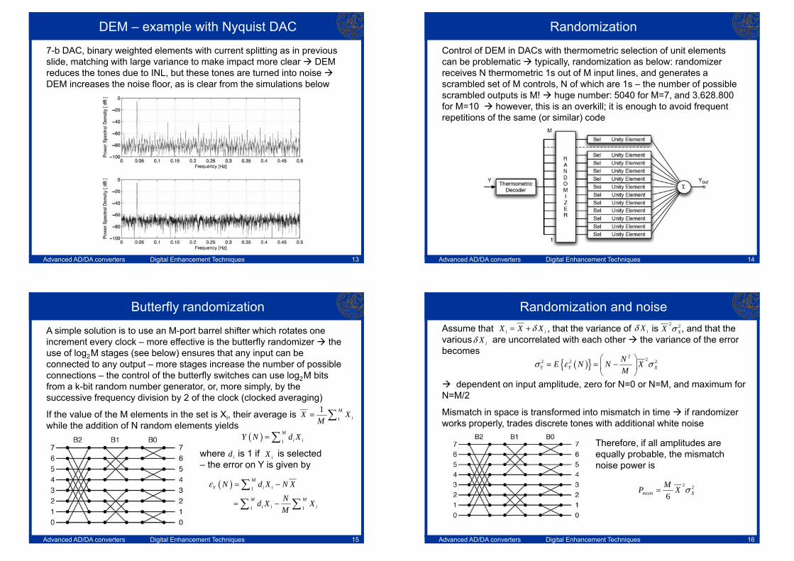
Single-bit vs. multi-bit – III
Rule-of-thumb: very roughly, the power used by a comparator is 1/20 of that used by an op-amp, operated at the same speed
More comparators also means more complexity, multi-bit digital signal processing in the decimator filter, and extra logic for digital calibration and dynamic element matching (if needed)
Typically, 3 to 15 comparators are used (i.e., up to 4 quantizer bits)
Multi-bit DAC usually implemented as a capacitive MDAC in a DT modulator
Advanced AD/DA converters Digital Enhancement Techniques 6
Multi-bit quantizers – many advantages
1) q-error reduced by 6dB for every added bit of resolution SQNR increased by same amount, and decimation/reconstruction filters easier to implement (less q-noise less filtering needed)
2) Feedback loops becomes more linear stability is more robust, performance closer to what linear analysis predicts
3) Improved stability NTF can be chosen more aggressively higher SQNR; also, larger input signals can be allowed (again, higher SQNR) – example: in a 5th-order single-bit modulator, stability considerations limit the SQNR to 60dB with OSR=16; with a 4-bitquantizer, lower q-noise and higher input signal yield SQNR=120dB!
4) DAC output changes less from sample to sample slew rate of opamps can be reduced power saving
5) Difference between input signal and DAC signals is smaller linearity requirement on input stage of the loop can be relaxed
6) In CT modulators, lower sensitivity to clock jitter
Advanced AD/DA converters Digital Enhancement Techniques 7
Improved linearity
Instantaneous gain k of the multi-bit quantizer is
( ) ( )( )
( ) ( )( )
( )( )1
v n y n e n e nk n
y n y n y n+
= = = +
Gain deviation from nominal value of 1 is at most , where is the LSB of the quantizer
Deviation is large for small y, which cannot overload the quantizer, and small for large y, where instability is most likely to occur. By contrast, in single-bit quantizers the instantaneous gain is 1/y(n), which can take any value and tends to 0 (instead of 1) for a large y, and we have seen that a small k is likely to result in instability for higher-order loops
( )2
y nΔ Δ
Advanced AD/DA converters Digital Enhancement Techniques 8
Multi-bit modulator – one major drawback
The multi-bit DAC is located on the feedback path any error eD in the DAC response is injected at the modulator input, and appears at the output without any shaping! This is the single (but momentous) disadvantage of the multi-bit approach
Of special concern is the fact that any distortion on the DAC signals results in a distorted output for an N-bit modulator linearity, the DAC needs to be at least N-bit linear DAC linearity is at most 12-bit without trimming other methods are needed to achieve a higher linearity (needed in e.g. audio applications) these methods are:
1) dual quantization 2) mismatch shaping 3) digital correction
Advanced AD/DA converters Digital Enhancement Techniques 9
1) – Dual quantization – I
Single-bit quantizer/DAC for outer feedback loop (error not shaped), and multi-bit for the inner loops (shaped error) modulator with two or more digital outputs, combined in a way that the large q-error of the single-bit quantizer is cancelled
Simplest example of this approach: Leslie-Singh modulator
Single-bit quantizer is linear, and the large q-error is converted by the multi-bit ADC in digital form and cancelled at the output with suitable expression for H1 and H2
Advanced AD/DA converters Digital Enhancement Techniques 10
Dual quantization – II
Extension of the approach – two-stage MASH below
The non-linearity of the 3b DAC will not introduce distortion, since only the q-error is processes by the 2nd stage; moreover, the error of this DAC will be filtered (along with e1) by the digital high-pass filter H2suppressed in the signal band the overall output is again (but now with a reduced e2)
Also: improved stability of 2nd stage more aggressive NTF2
( ) ( ) ( ) ( ) ( ) ( ) ( )1 2 1 2 2W z STF z STF z U z NTF z NTF z E z= −
Advanced AD/DA converters Digital Enhancement Techniques 11
Dual quantization with single-loop modulator
Example in a 3rd-order modulator N-bit DAC in the innermost loop its non-linearity (ED) is shaped by the transfer function of the first two integrators negligible if OSR is high
Also here the two outputs can be combined to cancel e1 we obtain (check it!):
Of course, cancellation of E1 relies on perfect matching between analog and digital transfer functions in practice, some single-bit q-noise will leak to the output (the impact of non-linearity in the multi-bit DAC can be further reduced by using one of the already discussed low-distortion architectures for the loop filter)
( ) ( ) ( ) ( ) ( ) ( )3 21 1 1 122 1 2 1 DV z z U z z E z z z E z− − − −= + − − −
RV =
Advanced AD/DA converters Digital Enhancement Techniques 12
2) – Dynamic element matching (DEM)
DAC components are made equal on average in the time domain! e.g. below: Iref is split into two equal currents I1 and I2 by M1 and M2, and R1 and R2 improve matching by reducing the impact of the MOS threshold mismatch – however, resistor mismatch impacts as well the four switches multiply Iref on average 50% of the time with +1, and 50% with –1 with a pseudo-random sequence mismatch becomes noise-like, and noise shaping improves further the technique
This and next several slides from Maloberti’s book
Advanced AD/DA converters Digital Enhancement Techniques 13
DEM – example with Nyquist DAC
7-b DAC, binary weighted elements with current splitting as in previous slide, matching with large variance to make impact more clear DEM reduces the tones due to INL, but these tones are turned into noise DEM increases the noise floor, as is clear from the simulations below
Advanced AD/DA converters Digital Enhancement Techniques 14
Randomization
Control of DEM in DACs with thermometric selection of unit elements can be problematic typically, randomization as below: randomizer receives N thermometric 1s out of M input lines, and generates a scrambled set of M controls, N of which are 1s – the number of possible scrambled outputs is M! huge number: 5040 for M=7, and 3.628.800 for M=10 however, this is an overkill; it is enough to avoid frequent repetitions of the same (or similar) code
Advanced AD/DA converters Digital Enhancement Techniques 15
Butterfly randomization
A simple solution is to use an M-port barrel shifter which rotates one increment every clock – more effective is the butterfly randomizer the use of log2M stages (see below) ensures that any input can be connected to any output – more stages increase the number of possible connections – the control of the butterfly switches can use log2M bits from a k-bit random number generator, or, more simply, by the successive frequency division by 2 of the clock (clocked averaging)
If the value of the M elements in the set is Xi, their average is while the addition of N random elements yields
1
1 MiX X
M= ∑
( ) 1
Mi iY N d X=∑
where is 1 if is selected – the error on Y is given by
id iX
( ) 1
1 1
MY i i
M Mi i i
N d X N X
Nd X XM
ε = −
= −
∑
∑ ∑
Advanced AD/DA converters Digital Enhancement Techniques 16
Randomization and noise Assume that , that the variance of is , and that the various are uncorrelated with each other the variance of the error becomes
dependent on input amplitude, zero for N=0 or N=M, and maximum for N=M/2
Mismatch in space is transformed into mismatch in time if randomizer works properly, trades discrete tones with additional white noise
i iX X Xδ= +
( ){ }2 22 2 2
Y Y XNE N N XM
σ ε σ⎛ ⎞= = −⎜ ⎟
⎝ ⎠
iXδ 2 2XX σ
iXδ
2 2
6mism XMP X σ=
Therefore, if all amplitudes are equally probable, the mismatch noise power is
Advanced AD/DA converters Digital Enhancement Techniques 17
Randomization and noise – II
The peak-to-peak amplitude of the output signal is the power of a full-scale sine wave is the SNR determined only by the mismatch error and OSR becomes
If M=8, OSR=1 (Nyquist-rate converter), and =2⋅10-3 SNR=62dB If M=8, OSR=32, and =2⋅10-3 SNR=77dB
The white-noise assumption depends on how effective the randomizer is – with b butterfly stages, the clocked averaging repeats the same pattern every 2b clock periods, introducing tones at fs/2b
– a pseudo-random number generator requires more hardware, but is more effective, especially when b is low
2
34 X
MSNR OSRσ
=
M X22 8M X
XσXσ
Advanced AD/DA converters Digital Enhancement Techniques 18
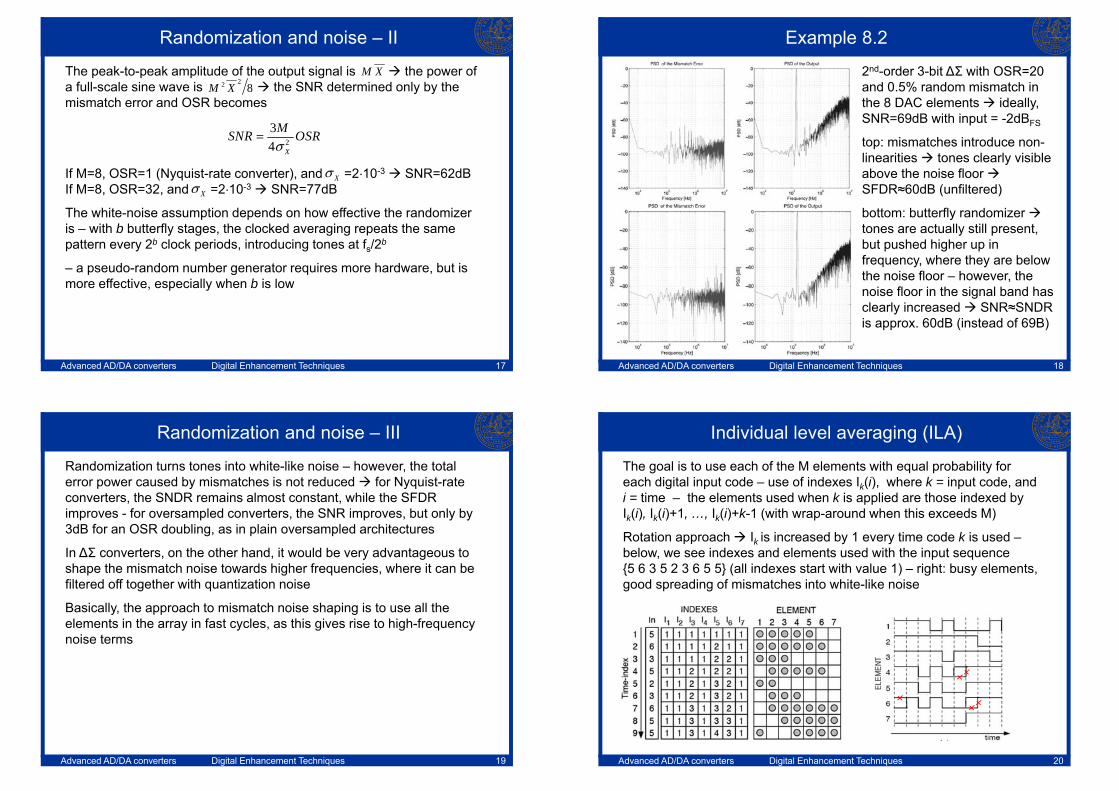
Example 8.2
2nd-order 3-bit ΔΣ with OSR=20 and 0.5% random mismatch in the 8 DAC elements ideally, SNR=69dB with input = -2dBFS
top: mismatches introduce non-linearities tones clearly visible above the noise floor SFDR≈60dB (unfiltered)
bottom: butterfly randomizer tones are actually still present, but pushed higher up in frequency, where they are below the noise floor – however, the noise floor in the signal band has clearly increased SNR≈SNDR is approx. 60dB (instead of 69B)
Advanced AD/DA converters Digital Enhancement Techniques 19
Randomization and noise – III
Randomization turns tones into white-like noise – however, the total error power caused by mismatches is not reduced for Nyquist-rate converters, the SNDR remains almost constant, while the SFDR improves - for oversampled converters, the SNR improves, but only by 3dB for an OSR doubling, as in plain oversampled architectures
In ΔΣ converters, on the other hand, it would be very advantageous to shape the mismatch noise towards higher frequencies, where it can be filtered off together with quantization noise
Basically, the approach to mismatch noise shaping is to use all the elements in the array in fast cycles, as this gives rise to high-frequency noise terms
Advanced AD/DA converters Digital Enhancement Techniques 20
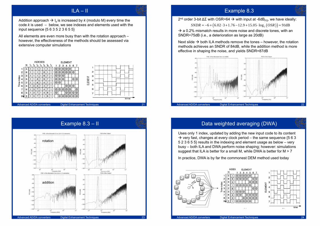
Individual level averaging (ILA)
The goal is to use each of the M elements with equal probability for each digital input code – use of indexes Ik(i), where k = input code, and i = time – the elements used when k is applied are those indexed by Ik(i), Ik(i)+1, …, Ik(i)+k-1 (with wrap-around when this exceeds M)
Rotation approach Ik is increased by 1 every time code k is used –below, we see indexes and elements used with the input sequence {5 6 3 5 2 3 6 5 5} (all indexes start with value 1) – right: busy elements, good spreading of mismatches into white-like noise
Advanced AD/DA converters Digital Enhancement Techniques 21
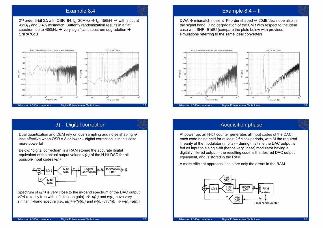
ILA – II
Addition approach Ik is increased by k (modulo M) every time the code k is used – below, we see indexes and elements used with the input sequence {5 6 3 5 2 3 6 5 5}
All elements are even more busy than with the rotation approach –however, the effectiveness of the methods should be assessed via extensive computer simulations
Advanced AD/DA converters Digital Enhancement Techniques 22
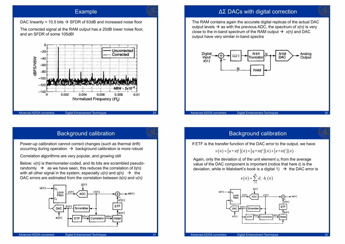
Example 8.32nd order 3-bit ΔΣ with OSR=64 with input at -6dBFS, we have ideally:
a 0.2% mismatch results in more noise and discrete tones, with an SNDR=75dB (i.e., a deterioration as large as 20dB)
Next slide both ILA methods remove the tones – however, the rotation methods achieves an SNDR of 84dB, while the addition method is more effective in shaping the noise, and yields SNDR=87dB
( )( )26 6.02 3 1.76 12.9 15.05 log 91dBSNDR OSR= − + ⋅ + − + ⋅ ≈
Advanced AD/DA converters Digital Enhancement Techniques 23
Example 8.3 – II
rotation
addition
Advanced AD/DA converters Digital Enhancement Techniques 24
Data weighted averaging (DWA)
Uses only 1 index, updated by adding the new input code to its content very fast, changes at every clock period – the same sequence {5 6 3
5 2 3 6 5 5} results in the indexing and element usage as below – very busy – both ILA and DWA perform noise shaping; however: simulations suggest that ILA is better for a small M, while DWA is better for M > 7
In practice, DWA is by far the commonest DEM method used today
Advanced AD/DA converters Digital Enhancement Techniques 25
Example 8.4
2nd order 3-bit ΣΔ with OSR=64, fS=20MHz fB=156kH with input at -6dBFS and 0.4% mismatch, Butterfly randomization results in a flat spectrum up to 400kHz very significant spectrum degradation SNR=70dB
Advanced AD/DA converters Digital Enhancement Techniques 26
Example 8.4 – II
DWA mismatch noise is 1st-order shaped 20dB/dec slope also in the signal band no degradation of the SNR with respect to the ideal case with SNR=91dB! (compare the plots below with previous simulations referring to the same ideal converter)
Advanced AD/DA converters Digital Enhancement Techniques 27
3) – Digital correction
Dual quantization and DEM rely on oversampling and noise shaping less effective when OSR = 8 or lower – digital correction is in this case more powerful
Below: “digital correction” is a RAM storing the accurate digital equivalent of the actual output values v’(n) of the N-bit DAC for all possible input codes v(n)
Spectrum of u(n) is very close to the in-band spectrum of the DAC output v’(n) (exactly true with infinite loop gain) u(n) and w(n) have very similar in-band spectra [i.e., u(n)=v’(v(n)) and w(n)=v’(v(n)) w(n)=u(n)]
Advanced AD/DA converters Digital Enhancement Techniques 28
Acquisition phase
At power up: an N-bit counter generates all input codes of the DAC, each code being held for at least 2M clock periods, with M the required linearity of the modulator (in bits) – during this time the DAC output is fed as input to a single-bit (hence very linear) modulator having a digitally filtered output – the resulting code is the desired DAC output equivalent, and is stored in the RAM
A more efficient approach is to store only the errors in the RAM
Advanced AD/DA converters Digital Enhancement Techniques 29
Example
DAC linearity = 10.5 bits SFDR of 63dB and increased noise floor
The corrected signal at the RAM output has a 20dB lower noise floor, and an SFDR of some 105dB!
Advanced AD/DA converters Digital Enhancement Techniques 30
ΔΣ DACs with digital correction
The RAM contains again the accurate digital replicas of the actual DAC output levels as with the previous ADC, the spectrum of x(n) is very close to the in-band spectrum of the RAM output x(n) and DAC output have very similar in-band spectra
Advanced AD/DA converters Digital Enhancement Techniques 31
Background calibration
Power-up calibration cannot correct changes (such as thermal drift) occurring during operation background calibration is more robust
Correlation algorithms are very popular, and growing still
Below: v(n) is thermometer-coded, and its bits are scrambled pseudo-randomly as we have seen, this reduces the correlation of b(n)with all other signal in the system, especially u(n) and q(n) the DAC errors are estimated from the correlation between b(n) and v(n)
Advanced AD/DA converters Digital Enhancement Techniques 32
Background calibration
( ) [ ]( ) [ ]( ) [ ]( )v n u stf n q ntf n e etf n= ∗ + ∗ + ∗
If ETF is the transfer function of the DAC error to the output, we have
( ) ( )1
M
i ii
e n d b n=
= ⋅∑
Again, only the deviation di of the unit element ui from the average value of the DAC component is important (notice that here di is the deviation, while in Maloberti’s book is a digital 1) the DAC error is
Advanced AD/DA converters Digital Enhancement Techniques 33
Background calibration
Estimate of ith DAC error di from the expected value of , where
Calling and , we obtain
( ) ( ){ } ( ) ( ){ } ( ) ( ){ } ( ) ( ){ }i i i iE v n b n E u n b n E q n b n E e n b n′ ′ ′ ′ ′ ′ ′⋅ = ⋅ + ⋅ + ⋅
( ) ( )iv n b n′⋅
( ) [ ]( )i ib n b etf n′ = ∗
( ) [ ]( )u n u stf n′ = ∗ ( ) [ ]( )q n q ntf n′ = ∗
Advanced AD/DA converters Digital Enhancement Techniques 34
Background calibration
Assuming that have zero mean, and that is uncorrelated with , the first two terms will be zero; assuming also that each is uncorrelated to all other , the last term simplifies to
, ,u q e′ ′ ′ib
,u q ibjb
( ) ( ){ } ( ) ( ) ( ) ( ){ }( ) ( ) ( ) ( ){ } ( ){ }2
i j j i
i i i i i
E e n b n E d b n etf n b n etf n
E d b n etf n b n etf n d E b n
′ ′ ⎡ ⎤⋅ = ∗ ⋅ ∗⎡ ⎤⎣ ⎦⎣ ⎦
′= ∗ ⋅ ∗ =⎡ ⎤ ⎡ ⎤ ⎡ ⎤⎣ ⎦ ⎣ ⎦ ⎣ ⎦
∑
( ) ( ){ }( ){ }2
ii
i
E v n b nd
E b n
′=
′⎡ ⎤⎣ ⎦from which we obtain
Advanced AD/DA converters Digital Enhancement Techniques 35
Background calibration
Thus, di can be found by accumulating the two products, and taking their ratio – this is performed by the correlator block, and the operation is referred to as correlation
di is stored in a RAM, periodically updated, and used to correct v(n) by subtracting the expected error e’(n) due to the DAC
Unfortunately, it is not really true that all bi are uncorrelated to all other sequences, and that all sequences have zero mean large residual error nevertheless, more advanced approaches can greatly reduce the harmful correlations and detect the desired one
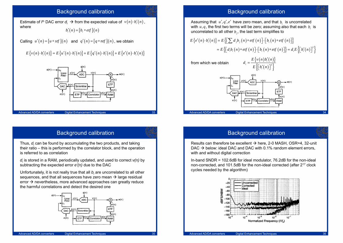
Advanced AD/DA converters Digital Enhancement Techniques 36
Background calibration
Results can therefore be excellent here, 2-0 MASH, OSR=4, 32-unit DAC below: ideal DAC and DAC with 0.1% random element errors, with and without digital correction
In-band SNDR = 102.6dB for ideal modulator, 76.2dB for the non-ideal non-corrected, and 101.5dB for the non-ideal corrected (after 217 clock cycles needed by the algorithm)