ΗΥ425 Αρχιτεκτονική Υπολογιστών Precise Exception Reorder Buffer Ιάκωβος Μαυροειδής
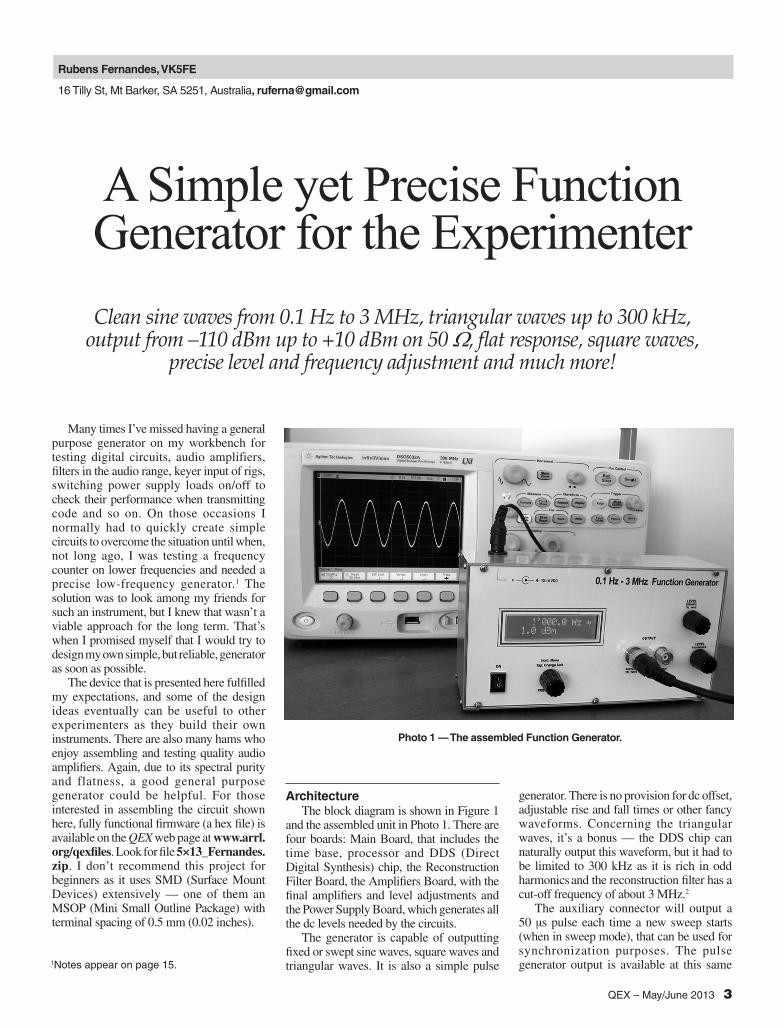
QEX – May/June 2013 3
Rubens Fernandes, VK5FE
16 Tilly St, Mt Barker, SA 5251, Australia, [email protected]
A Simple yet Precise Function Generator for the ExperimenterClean sine waves from 0.1 Hz to 3 MHz, triangular waves up to 300 kHz,
output from –110 dBm up to +10 dBm on 50 Ω, flat response, square waves, precise level and frequency adjustment and much more!
Many times I’ve missed having a general purpose generator on my workbench for testing digital circuits, audio amplifiers, filters in the audio range, keyer input of rigs, switching power supply loads on/off to check their performance when transmitting code and so on. On those occasions I normally had to quickly create simple circuits to overcome the situation until when, not long ago, I was testing a frequency counter on lower frequencies and needed a precise low-frequency generator.1 The solution was to look among my friends for such an instrument, but I knew that wasn’t a viable approach for the long term. That’s when I promised myself that I would try to design my own simple, but reliable, generator as soon as possible.
The device that is presented here fulfilled my expectations, and some of the design ideas eventually can be useful to other experi menters as they build their own instruments. There are also many hams who enjoy assembling and testing quality audio amplifiers. Again, due to its spectral purity and flatness, a good general purpose generator could be helpful. For those interested in assembling the circuit shown here, fully functional firmware (a hex file) is available on the QEX web page at www.arrl.org/qexfiles. Look for file 5×13_Fernandes.zip. I don’t recommend this project for beginners as it uses SMD (Surface Mount Devices) extensively — one of them an MSOP (Mini Small Outline Package) with terminal spacing of 0.5 mm (0.02 inches).
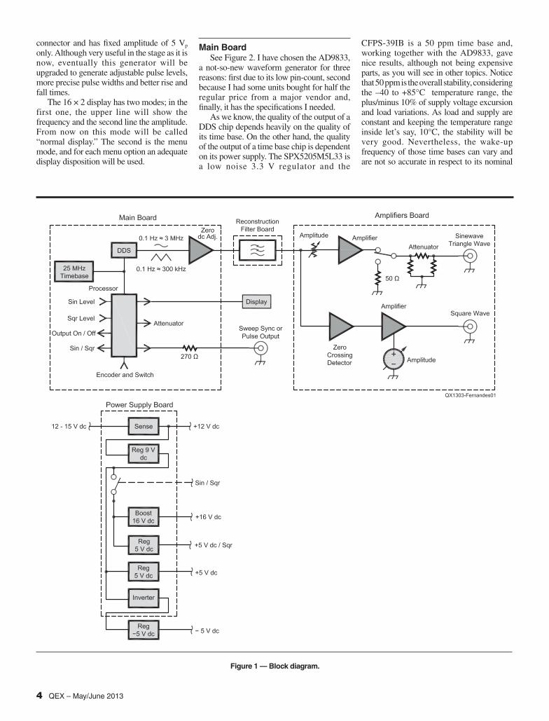
ArchitectureThe block diagram is shown in Figure 1
and the assembled unit in Photo 1. There are four boards: Main Board, that includes the time base, processor and DDS (Direct Digital Synthesis) chip, the Reconstruction Filter Board, the Amplifiers Board, with the final amplifiers and level adjustments and the Power Supply Board, which generates all the dc levels needed by the circuits.
The generator is capable of outputting fixed or swept sine waves, square waves and triangular waves. It is also a simple pulse
generator. There is no provision for dc offset, adjustable rise and fall times or other fancy waveforms. Concerning the triangular waves, it’s a bonus — the DDS chip can naturally output this waveform, but it had to be limited to 300 kHz as it is rich in odd harmonics and the reconstruction filter has a cut-off frequency of about 3 MHz.2
The auxiliary connector will output a 50 µs pulse each time a new sweep starts (when in sweep mode), that can be used for synchronization purposes. The pulse generator output is available at this same 1Notes appear on page 15.
Photo 1 — The assembled Function Generator.
4 QEX – May/June 2013
connector and has fixed amplitude of 5 Vp only. Although very useful in the stage as it is now, eventually this generator will be upgraded to generate adjustable pulse levels, more precise pulse widths and better rise and fall times.
The 16 × 2 display has two modes; in the first one, the upper line will show the frequency and the second line the amplitude. From now on this mode will be called “normal display.” The second is the menu mode, and for each menu option an adequate display disposition will be used.
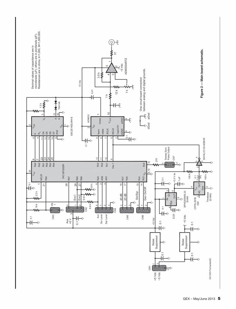
Main BoardSee Figure 2. I have chosen the AD9833,
a not-so-new waveform generator for three reasons: first due to its low pin-count, second because I had some units bought for half the regular price from a major vendor and, finally, it has the specifications I needed.
As we know, the quality of the output of a DDS chip depends heavily on the quality of its time base. On the other hand, the quality of the output of a time base chip is dependent on its power supply. The SPX5205M5L33 is a low noise 3.3 V regulator and the
CFPS-39IB is a 50 ppm time base and, working together with the AD9833, gave nice results, although not being expensive parts, as you will see in other topics. Notice that 50 ppm is the overall stability, considering the –40 to +85°C temperature range, the plus/minus 10% of supply voltage excursion and load variations. As load and supply are constant and keeping the temperature range inside let’s say, 10°C, the stability will be very good. Nevertheless, the wake-up frequency of those time bases can vary and are not so accurate in respect to its nominal
Figure 1 — Block diagram.
QEX – May/June 2013 5
Figu
re 2
— M
ain
boar
d sc
hem
atic
.
6 QEX – May/June 2013
frequency. This creates an accuracy problem as the frequency output by the DDS is a fraction of the time base frequency. The solution was to include a calibration procedure to correct the reference frequency used in the calculations that have to be done each time the frequency in the chip is changed.
The inverter/Schmidt trigger was used mainly as a level adapter, as the time base uses a 3.3 V dc power supply and the processor and DDS are working with 5 V dc. The two components named NS are noise suppressors, used just as a precaution. The display is a conventional 16 × 2 unit, white-over-blue characters (less power consump-tion). For simplicity I avoided the use of a variable dc level for the backlight LEDs, using instead two diodes to reduce the voltage. With the same philosophy, the contrast adjustment is made with two fixed resistors. In fact, just the 1.2 kΩ resistor to ground should do the job. The external encoder is connected through CN2 and its switch via CN3. The AD8055 is a 300 MHz voltage feedback amplifier connected to have a voltage gain of about 4 and is also responsible for the 0 V dc level adjustment.
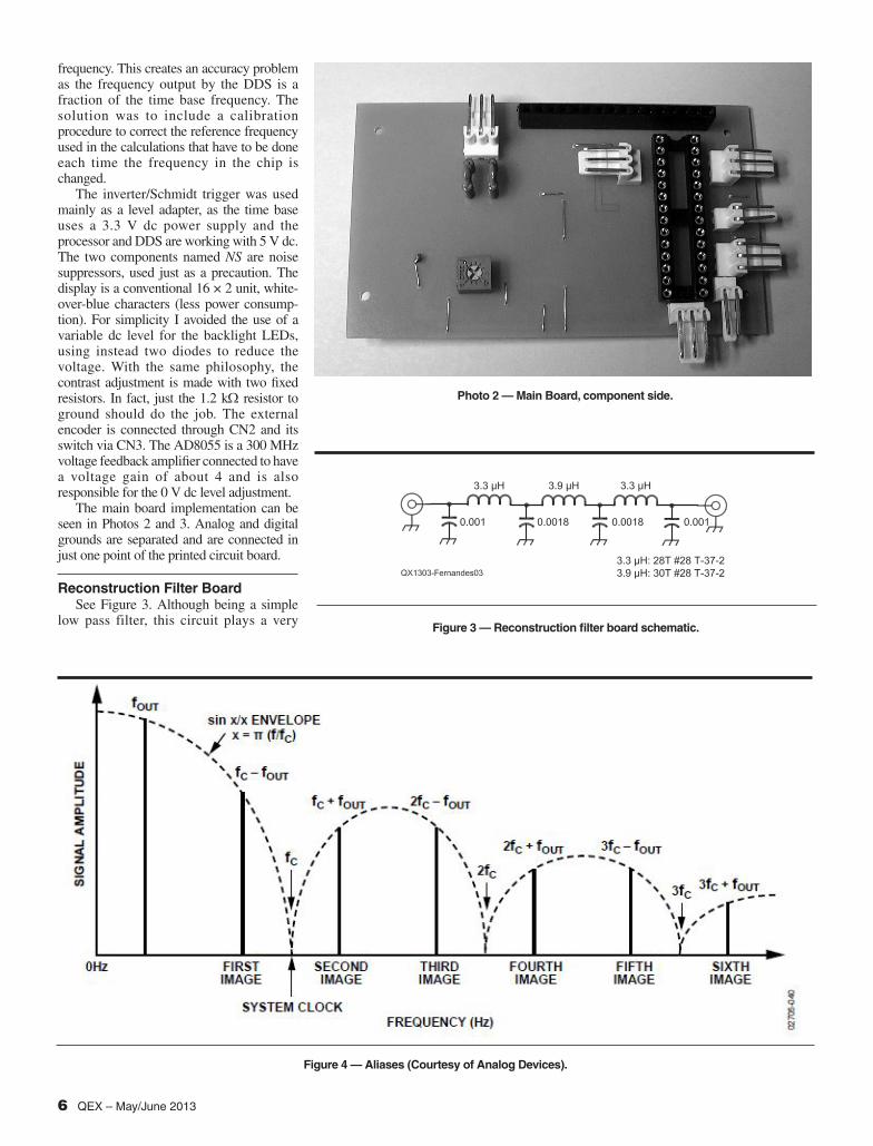
The main board implementation can be seen in Photos 2 and 3. Analog and digital grounds are separated and are connected in just one point of the printed circuit board.
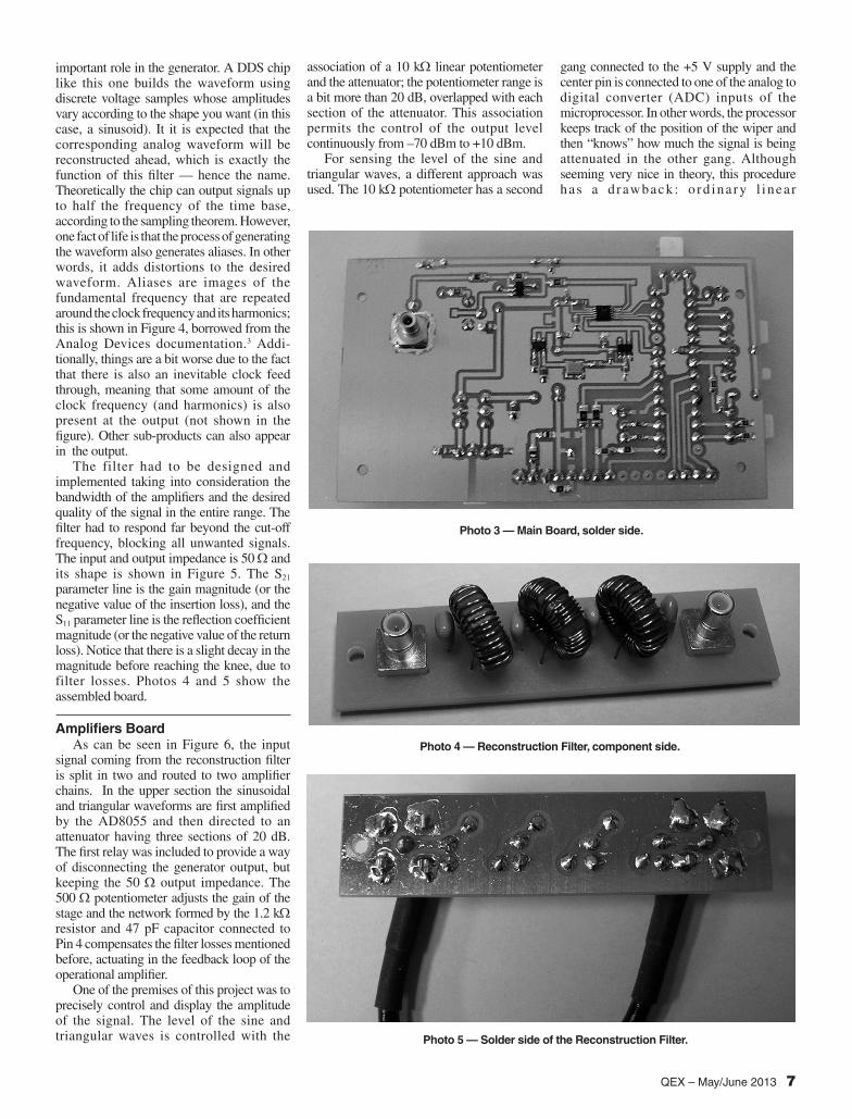
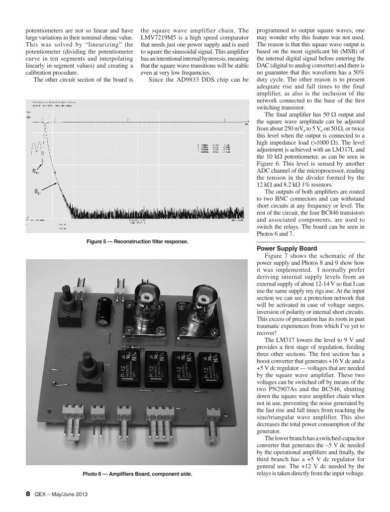
Reconstruction Filter BoardSee Figure 3. Although being a simple
low pass filter, this circuit plays a very
Figure 4 — Aliases (Courtesy of Analog Devices).
Figure 3 — Reconstruction filter board schematic.
Photo 2 — Main Board, component side.
QEX – May/June 2013 7
important role in the generator. A DDS chip like this one builds the waveform using discrete voltage samples whose amplitudes vary according to the shape you want (in this case, a sinusoid). It it is expected that the corresponding analog waveform will be reconstructed ahead, which is exactly the function of this filter — hence the name. Theoretically the chip can output signals up to half the frequency of the time base, according to the sampling theorem. However, one fact of life is that the process of generating the waveform also generates aliases. In other words, it adds distortions to the desired waveform. Aliases are images of the fundamental frequency that are repeated around the clock frequency and its harmonics; this is shown in Figure 4, borrowed from the Analog Devices documentation.3 Addi-tionally, things are a bit worse due to the fact that there is also an inevitable clock feed through, meaning that some amount of the clock frequency (and harmonics) is also present at the output (not shown in the figure). Other sub-products can also appear in the output.
The filter had to be designed and implemented taking into consideration the bandwidth of the amplifiers and the desired quality of the signal in the entire range. The filter had to respond far beyond the cut-off frequency, blocking all unwanted signals. The input and output impedance is 50 Ω and its shape is shown in Figure 5. The S21 parameter line is the gain magnitude (or the negative value of the insertion loss), and the S11 parameter line is the reflection coefficient magnitude (or the negative value of the return loss). Notice that there is a slight decay in the magnitude before reaching the knee, due to filter losses. Photos 4 and 5 show the assembled board.
Amplifiers BoardAs can be seen in Figure 6, the input
signal coming from the reconstruction filter is split in two and routed to two amplifier chains. In the upper section the sinusoidal and triangular waveforms are first amplified by the AD8055 and then directed to an attenuator having three sections of 20 dB. The first relay was included to provide a way of disconnecting the generator output, but keeping the 50 Ω output impedance. The 500 Ω potentiometer adjusts the gain of the stage and the network formed by the 1.2 kΩ resistor and 47 pF capacitor connected to Pin 4 compensates the filter losses mentioned before, actuating in the feedback loop of the operational amplifier.
One of the premises of this project was to precisely control and display the amplitude of the signal. The level of the sine and triangular waves is controlled with the
Photo 3 — Main Board, solder side.
Photo 4 — Reconstruction Filter, component side.
Photo 5 — Solder side of the Reconstruction Filter.
association of a 10 kΩ linear potentiometer and the attenuator; the potentiometer range is a bit more than 20 dB, overlapped with each section of the attenuator. This association permits the control of the output level continuously from –70 dBm to +10 dBm.
For sensing the level of the sine and triangular waves, a different approach was used. The 10 kΩ potentiometer has a second
gang connected to the +5 V supply and the center pin is connected to one of the analog to digital converter (ADC) inputs of the microprocessor. In other words, the processor keeps track of the position of the wiper and then “knows” how much the signal is being attenuated in the other gang. Although seeming very nice in theory, this procedure has a d rawback : o rd ina ry l inea r
8 QEX – May/June 2013
potenti ometers are not so linear and have large variations in their nominal ohmic value. This was solved by “linearizing” the potentiometer (dividing the potentiometer curve in ten segments and interpolating linearly in-segment values) and creating a calibration procedure.
The other circuit section of the board is
programmed to output square waves, one may wonder why this feature was not used. The reason is that this square wave output is based on the most significant bit (MSB) of the internal digital signal before entering the DAC (digital to analog converter) and there is no guarantee that this waveform has a 50% duty cycle. The other reason is to present adequate rise and fall times to the final amplifier, as also is the inclusion of the network connected to the base of the first switching transistor.
The final amplifier has 50 Ω output and the square wave amplitude can be adjusted from about 250 mVp to 5 Vp on 50 Ω, or twice this level when the output is connected to a high impedance load (>1000 Ω). The level adjustment is achieved with an LM317L and the 10 kΩ potentiometer, as can be seen in Figure 6. This level is sensed by another ADC channel of the microprocessor, reading the tension in the divider formed by the 12 kΩ and 8.2 kΩ 1% resistors.
The outputs of both amplifiers are routed to two BNC connectors and can withstand short circuits at any frequency or level. The rest of the circuit, the four BC846 transistors and associated components, are used to switch the relays. The board can be seen in Photos 6 and 7.
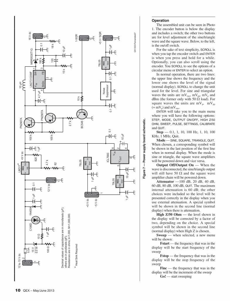
Power Supply BoardFigure 7 shows the schematic of the
power supply and Photos 8 and 9 show how it was implemented. I normally prefer deriving internal supply levels from an external supply of about 12-14 V so that I can use the same supply my rigs use. At the input section we can see a protection network that will be activated in case of voltage surges, inversion of polarity or internal short circuits. This excess of precaution has its roots in past traumatic experiences from which I’ve yet to recover!
The LM317 lowers the level to 9 V and provides a first stage of regulation, feeding three other sections. The first section has a boost converter that generates +16 V dc and a +5 V dc regulator — voltages that are needed by the square wave amplifier. These two voltages can be switched off by means of the two PN2907As and the BC546, shutting down the square wave amplifier chain when not in use, preventing the noise generated by the fast rise and fall times from reaching the sine/triangular wave amplifier. This also decreases the total power consumption of the generator.
The lower branch has a switched-capacitor converter that generates the –5 V dc needed by the operational amplifiers and finally, the third branch has a +5 V dc regulator for general use. The +12 V dc needed by the relays is taken directly from the input voltage.
Figure 5 — Reconstruction filter response.
Photo 6 — Amplifiers Board, component side.
the square wave amplifier chain. The LMV7219M5 is a high speed comparator that needs just one power supply and is used to square the sinusoidal signal. This amplifier has an intentional internal hysteresis, meaning that the square wave transitions will be stable even at very low frequencies.
Since the AD9833 DDS chip can be
QEX – May/June 2013 9
Figu
re 6
— A
mpl
ifier
s bo
ard
sche
mat
ic.
10 QEX – May/June 2013
Figu
re 7
— P
ower
sup
ply
boar
d sc
hem
atic
.
OperationThe assembled unit can be seen in Photo
1. The encoder button is below the display and includes a switch; the other two buttons are for level adjustment of the sine/triangle wave and the square wave. Below, to the left, is the on/off switch.
For the sake of text simplicity, SCROLL is when you tap the encoder switch and ENTER is when you press and hold for a while. Optionally, you can also scroll using the encoder. You SCROLL to see the options of a circular menu or ENTER to select an option.
In normal operation, there are two lines: the upper line shows the frequency and the lower one shows the level of the signal (normal display). SCROLL to change the unit used for the level. For sine and triangular waves the units are mVrms, mVpp, mVp and dBm (the former only with 50 Ω load). For square waves the units are mVp, mVpp (= mVp) and mVrms.
ENTER will take you to the main menu where you will have the following options: STEP, MODE, OUTPUT ON/OFF, HIGH Z/50 OHM, SWEEP, PULSE, SETTINGS, CALIBRATE and QUIT.
Step — 0.1, 1, 10, 100 Hz, 1, 10, 100 KHz, 1 MHz, Quit.
Mode — SINE, SQUARE, TRIANGLE, QUIT. When chosen, a corresponding symbol will be shown in the last position of the first line when in normal display. When the mode is sine or triangle, the square wave amplifiers will be powered down and vice versa.
Output Off/Output On — When the wave is disconnected, the sine/triangle output will still have 50 Ω and the square wave amplifier chain will be powered down.
Attenuator —100 dB, 20 dB, 40 dB, 60 dB, 80 dB, 100 dB, QUIT. The maximum internal attenuation is 60 dB; the other choices were included so the level will be presented correctly in the display when you use external attenuation. A special symbol will be shown in the second line (normal display) when there is attenuation.
High Z/50 Ohm — the level shown in the display will be corrected by a factor of two, depending on the choice. A special symbol will be shown in the second line (normal display) when High Z is chosen.
Sweep — when selected, a new menu will be shown:
Fstart — the frequency that was in the display will be the start frequency of the sweep
Fstop — the frequency that was in the display will be the stop frequency of the sweep
Finc — the frequency that was in the display will be the increment of the sweep
Go! — start sweeping
QEX – May/June 2013 11
Quit — quit the main menuPulse — when selected, a new menu will
be shown: ON time — enter to choose the ON
time of the pulses. Now scrolling will change the unit (ms, s, µs) and the encoder will change the time, inside the allowed limits.
OFF time — enter to choose the OFF time of the train of pulses. Same procedure as before.
Burst — enter to choose how many pulses to output — 0 means continuous.
Go! — start outputting pulses in the auxiliary connector.
Quit — quit the main menu.Settings — when selected, a new menu
will be shown: Save Settings — all settings that are
active at this moment will be saved and will be the new set of default settings.
Default Settings — all programmed settings will be replaced, without warning, by the “factory” default settings and will be the new set of default settings. This won’t affect the calibration data.
Quit – quit the main menu.Calibrate — when selected, a new menu
will be shown: Frequency — modify the offset using
the encoder and enter to input ADC ref. Level – modify the voltage
using the encoder and enter to input Min Sin Level – modify the minimum
level using the encoder and enter to input Sine Samples — for each of the ten
entries, modify using the encoder and enter to input
Quit – quit to the main menuQuit – quit the main menu
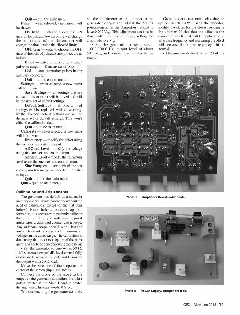
Calibration and AdjustmentsThe generator has default data saved in
memory and will work reasonably without the need of calibration (except for the first item below). Nevertheless, to reach top per-formance, it is necessary to patiently calibrate the unit. For this, you will need a good multimeter, a calibrated counter and a scope. Any ordinary scope should work, but the multimeter must be capable of measuring ac voltages in the audio range. The calibration is done using the CALIBRATE option of the main menu and has to be done following these steps:
• Set the generator to sine wave, 50 Ω, 1 kHz, attenuation to 0 dB, level control fully clockwise (maximum output) and terminate the output with a 50 Ω load.
Move the zero line of the scope to the center of the screen (input grounded).
Connect the probe of the scope to the output of the generator and adjust the 1 kΩ potentiometer in the Main Board to center the sine wave. In other words, 0 V dc.
Without touching the generator controls,
Photo 7 — Amplifiers Board, solder side.
Photo 8 — Power Supply, component side.
set the multimeter to ac, connect to the generator output and adjust the 500 Ω potentiometer in the Amplifiers Board to have 0.707 Vrms. This adjustment can also be done with a calibrated scope, setting the amplitude to 2 Vpp.
• Set the generator to sine wave, 1,000,000.0 Hz, output level of about 50 mVrms and connect the counter to the output.
Go to the CALIBRATE menu, choosing the option FREQUENCY. Using the encoder, modify the offset for the closest reading in the counter. Notice that the offset is the correction, in Hz, that will be applied to the time base frequency and increasing the offset will decrease the output frequency. This is normal.
• Measure the dc level at pin 20 of the
12 QEX – May/June 2013
microprocessor (+5.00 V dc supply nominal). Go to the CALIBRATE menu, choosing the option ADC REF. LEVEL. With the encoder, set the correct level. Press ENTER.
• Set the generator to sine wave, 1 kHz, level control fully anticlockwise (minimum level), 0 dB attenuation, output terminated with 50 Ω. Set the multimeter to ac, connect to the output and write down the reading. Go
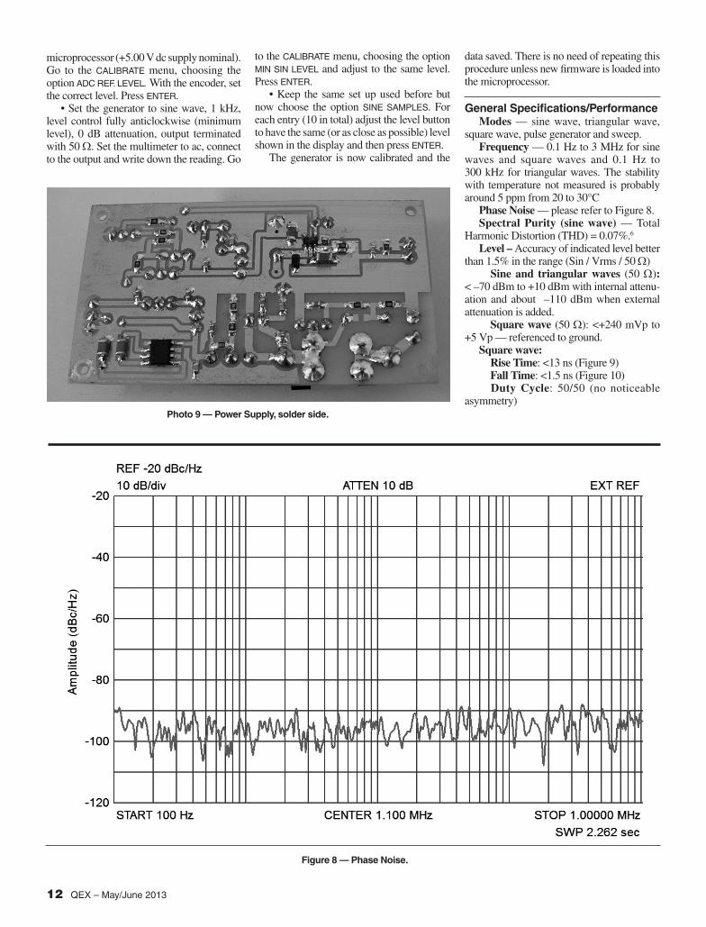
Photo 9 — Power Supply, solder side.
Figure 8 — Phase Noise.
to the CALIBRATE menu, choosing the option MIN SIN LEVEL and adjust to the same level. Press ENTER.
• Keep the same set up used before but now choose the option SINE SAMPLES. For each entry (10 in total) adjust the level button to have the same (or as close as possible) level shown in the display and then press ENTER.
The generator is now calibrated and the
data saved. There is no need of repeating this procedure unless new firmware is loaded into the microprocessor.
General Specifications/PerformanceModes — sine wave, triangular wave,
square wave, pulse generator and sweep.Frequency — 0.1 Hz to 3 MHz for sine
waves and square waves and 0.1 Hz to 300 kHz for triangular waves. The stability with temperature not measured is probably around 5 ppm from 20 to 30°C
Phase Noise — please refer to Figure 8. Spectral Purity (sine wave) — Total
Harmonic Distortion (THD) = 0.07%.6
Level – Accuracy of indicated level better than 1.5% in the range (Sin / Vrms / 50 Ω)
Sine and triangular waves (50 Ω): < –70 dBm to +10 dBm with internal attenu-ation and about –110 dBm when external attenuation is added.
Square wave (50 Ω): <+240 mVp to +5 Vp — referenced to ground.
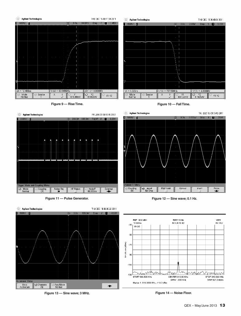
Square wave: Rise Time: <13 ns (Figure 9) Fall Time: <1.5 ns (Figure 10) Duty Cycle: 50/50 (no noticeable
asymmetry)
QEX – May/June 2013 13
Figure 9 — Rise Time. Figure 10 — Fall Time.
Figure 11 — Pulse Generator. Figure 12 — Sine wave; 0.1 Hz.
Figure 13 — Sine wave; 3 MHz. Figure 14 — Noise Floor.
14 QEX – May/June 2013
Ringing/Undershoot: <2%Pulse generator — ON and OFF time
adjustable from 10 µs to 65 s. Output on the auxiliary connector. (Figure 11)
Attenuator — only for sine waves and triangular waves, from 0 dB to 60 dB. Accepts additional 40 dB of external attenuation.
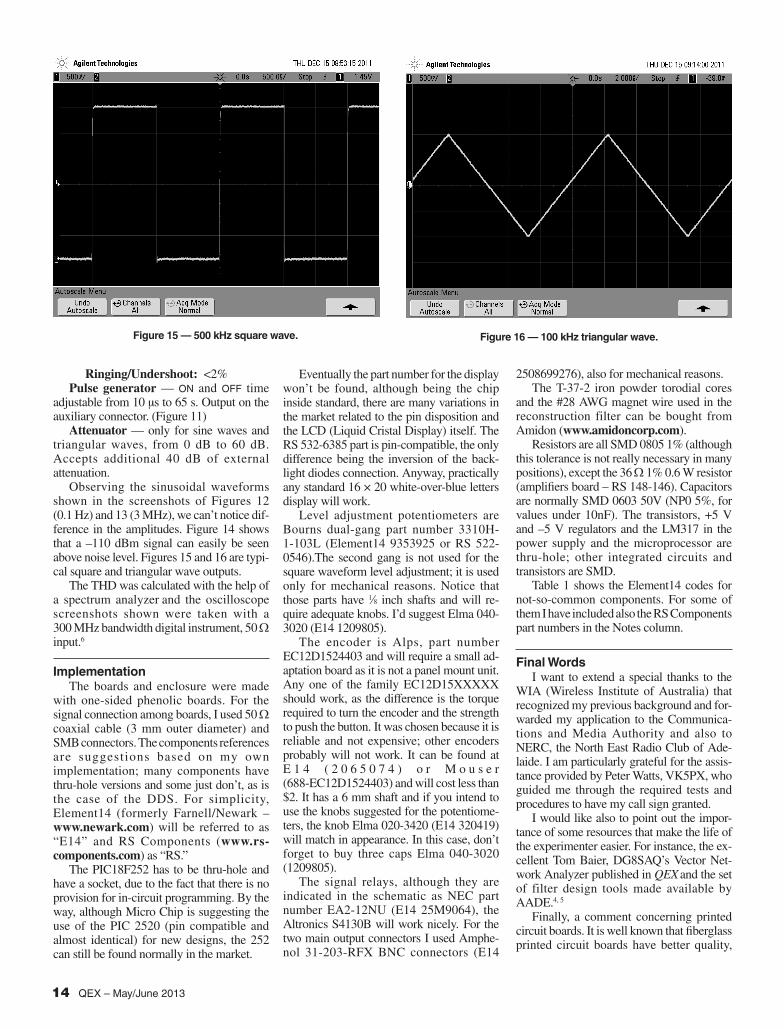
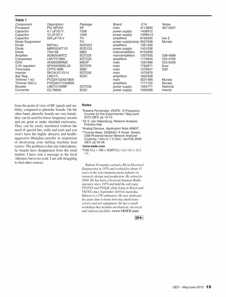
Observing the sinusoidal waveforms shown in the screenshots of Figures 12 (0.1 Hz) and 13 (3 MHz), we can’t notice dif-ference in the amplitudes. Figure 14 shows that a –110 dBm signal can easily be seen above noise level. Figures 15 and 16 are typi-cal square and triangular wave outputs.
The THD was calculated with the help of a spectrum analyzer and the oscilloscope screenshots shown were taken with a 300 MHz bandwidth digital instrument, 50 Ω input.6
ImplementationThe boards and enclosure were made
with one-sided phenolic boards. For the signal connection among boards, I used 50 Ω coaxial cable (3 mm outer diameter) and SMB connectors. The components references are suggestions based on my own implementation; many components have thru-hole versions and some just don’t, as is the case of the DDS. For simplicity, Element14 (formerly Farnell/Newark – www.newark.com) will be referred to as “E14” and RS Components (www.rs-components.com) as “RS.”
The PIC18F252 has to be thru-hole and have a socket, due to the fact that there is no provision for in-circuit programming. By the way, although Micro Chip is suggesting the use of the PIC 2520 (pin compatible and almost identical) for new designs, the 252 can still be found normally in the market.
Eventually the part number for the display won’t be found, although being the chip inside standard, there are many variations in the market related to the pin disposition and the LCD (Liquid Cristal Display) itself. The RS 532-6385 part is pin-compatible, the only difference being the inversion of the back-light diodes connection. Anyway, practically any standard 16 × 20 white-over-blue letters display will work.
Level adjustment potentiometers are Bourns dual-gang part number 3310H-1-103L (Element14 9353925 or RS 522-0546).The second gang is not used for the square waveform level adjustment; it is used only for mechanical reasons. Notice that those parts have 1⁄8 inch shafts and will re-quire adequate knobs. I’d suggest Elma 040-3020 (E14 1209805).
The encoder is Alps, part number EC12D1524403 and will require a small ad-aptation board as it is not a panel mount unit. Any one of the family EC12D15XXXXX should work, as the difference is the torque required to turn the encoder and the strength to push the button. It was chosen because it is reliable and not expensive; other encoders probably will not work. It can be found at E 1 4 ( 2 0 6 5 0 7 4 ) o r M o u s e r (688-EC12D1524403) and will cost less than $2. It has a 6 mm shaft and if you intend to use the knobs suggested for the potentiome-ters, the knob Elma 020-3420 (E14 320419) will match in appearance. In this case, don’t forget to buy three caps Elma 040-3020 (1209805).
The signal relays, although they are indicated in the schematic as NEC part number EA2-12NU (E14 25M9064), the Altronics S4130B will work nicely. For the two main output connectors I used Amphe-nol 31-203-RFX BNC connectors (E14
Figure 15 — 500 kHz square wave. Figure 16 — 100 kHz triangular wave.
2508699276), also for mechanical reasons.The T-37-2 iron powder torodial cores
and the #28 AWG magnet wire used in the reconstruction filter can be bought from Amidon (www.amidoncorp.com).
Resistors are all SMD 0805 1% (although this tolerance is not really necessary in many positions), except the 36 Ω 1% 0.6 W resistor (amplifiers board – RS 148-146). Capacitors are normally SMD 0603 50V (NP0 5%, for values under 10nF). The transistors, +5 V and –5 V regulators and the LM317 in the power supply and the microprocessor are thru-hole; other integrated circuits and transistors are SMD.
Table 1 shows the Element14 codes for not-so-common components. For some of them I have included also the RS Components part numbers in the Notes column.
Final WordsI want to extend a special thanks to the
WIA (Wireless Institute of Australia) that recognized my previous background and for-warded my application to the Communica-tions and Media Authority and also to NERC, the North East Radio Club of Ade-laide. I am particularly grateful for the assis-tance provided by Peter Watts, VK5PX, who guided me through the required tests and procedures to have my call sign granted.
I would like also to point out the impor-tance of some resources that make the life of the experimenter easier. For instance, the ex-cellent Tom Baier, DG8SAQ’s Vector Net-work Analyzer published in QEX and the set of filter design tools made available by AADE.4, 5
Finally, a comment concerning printed circuit boards. It is well known that fiberglass printed circuit boards have better quality,
QEX – May/June 2013 15
Table 1Component Description Package Board E14 Notes Processor PIC18F252 SP main 4113690 467-2047Capacitor 4.7 µF/25 V 1206 power supply 1458912Capacitor 10 µF/25 V 1206 power supply 10R6412Capacitor 220 µF/16 V TH amplifiers 8126305 low ZNoise Suppressor TH power supply/amp 9527508 MurataDiode BAT54J SOD323 amplifiers 1261336Diode MBR0530T1G SOD123 power supply 1431036Diode TS4148 0805 main/amplifiers 8150206Amplifier AD8055ARTZ SOT235 main/amplifiers 1267935 538-4088Comparator LMV7219M5 SOT235 amplifiers 1174640 534-4765DDS AD9833BRMZ MSOP main 1581966 523-64283.3V regulator SPX5205M5L33 SOT235 main 1762871 ExarTime base CFPS-39IB SMD main 1276647 IQDInverter SN74LVC1G14 SOT235 main 1470878Adj. Reg. LM317L SOIC amplifiers 1652326Trimmer 1 kΩ PVZ2A102A01B00 main 3531466 MurataTrimmer 500 Ω PVZ2A471C04B00 amplifiers 1771720 MurataBooster LM27313XMF SOT235 power supply 1564771 NationalConverter ICL7660A SOIC power supply 1562068 Intersil
from the point of view of RF signals and sta-bility, compared to phenolic boards. On the other hand, phenolic boards are very handy: they can be used for lower frequency circuits and are great to make shielded enclosures. They can be easily machined without the need of special bits, mills and tools and you won’t have the highly abrasive and health-aggressive fiberglass powder in suspension or destroying your milling machine lead screws. The problem is that one sided pheno-lic boards have disappeared from the retail market; I have sent a message to the local Altronics but to no avail. I am still struggling to find other sources.
Notes1Rubens Fernandes, VK5FE, “A Frequency
Counter for the Experimenter,” May/June 2010 QEX, pp 10-15.
2 M. E. van Valkenburg, Network Analysis, Prentice-Hall.
3Analog Devices, Application Note AN837.4 Thomas Baier, DG8SAQ “A Small, Simple,
USB-Powered Vector Network Analyzer Covering 1 kHz to 1.3 GHz,” Jan/Feb 2009 QEX, pp 33-36.
5www.aade.com6THD (%) = 100 × SQRT(V2
2 +V32 +V4
2 + V52)
/ V1
Rubens Fernandes earned a BS in Electrical Engineering in 1970 and worked for about 31 years in the telecommunications industry in research, design and production. He retired in 2004. He has been a licensed Amateur Radio operator since 1979 and held the call signs PY2FXJ and PY2QE while living in Brazil and VK5FE since September 2010 in Australia. Rubens is a CW enthusiast. He now dedicates his spare time to home brewing small trans-ceivers and test equipment. He has a small workshop that includes mechanical, electrical and software facilities. (www.VK5FE.com)