A 42-Gb/s Decision Circuit in 0.13μm CMOS
4
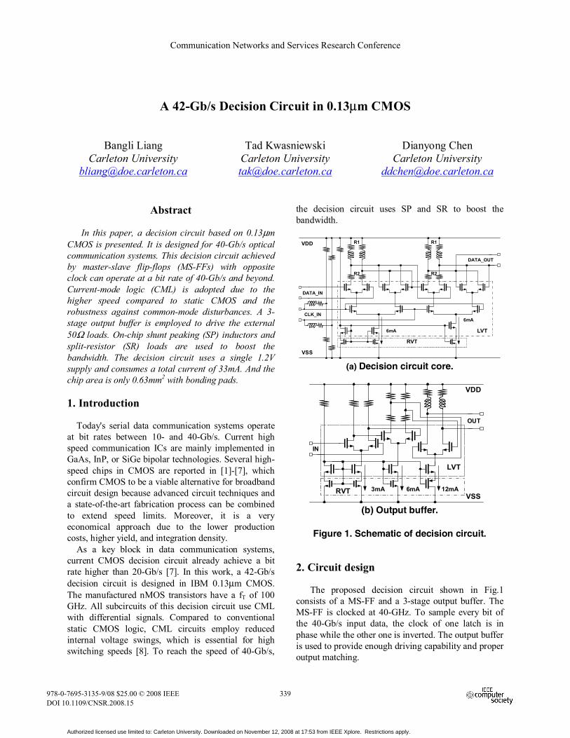
A 42-Gb/s Decision Circuit in 0.13µm CMOS Bangli Liang Carleton University [email protected] Tad Kwasniewski Carleton University [email protected] Dianyong Chen Carleton University [email protected] Abstract In this paper, a decision circuit based on 0.13µm CMOS is presented. It is designed for 40-Gb/s optical communication systems. This decision circuit achieved by master-slave flip-flops (MS-FFs) with opposite clock can operate at a bit rate of 40-Gb/s and beyond. Current-mode logic (CML) is adopted due to the higher speed compared to static CMOS and the robustness against common-mode disturbances. A 3- stage output buffer is employed to drive the external 50Ω loads. On-chip shunt peaking (SP) inductors and split-resistor (SR) loads are used to boost the bandwidth. The decision circuit uses a single 1.2V supply and consumes a total current of 33mA. And the chip area is only 0.63mm 2 with bonding pads. 1. Introduction Today's serial data communication systems operate at bit rates between 10- and 40-Gb/s. Current high speed communication ICs are mainly implemented in GaAs, InP, or SiGe bipolar technologies. Several high- speed chips in CMOS are reported in [1]-[7], which confirm CMOS to be a viable alternative for broadband circuit design because advanced circuit techniques and a state-of-the-art fabrication process can be combined to extend speed limits. Moreover, it is a very economical approach due to the lower production costs, higher yield, and integration density. As a key block in data communication systems, current CMOS decision circuit already achieve a bit rate higher than 20-Gb/s [7]. In this work, a 42-Gb/s decision circuit is designed in IBM 0.13µm CMOS. The manufactured nMOS transistors have a f T of 100 GHz. All subcircuits of this decision circuit use CML with differential signals. Compared to conventional static CMOS logic, CML circuits employ reduced internal voltage swings, which is essential for high switching speeds [8]. To reach the speed of 40-Gb/s, the decision circuit uses SP and SR to boost the bandwidth. DATA_OUT CLK_IN LVT RVT VDD VSS 6mA 6mA DATA_IN R1 R1 R2 R2 (a) Decision circuit core. OUT IN LVT RVT 6mA 3mA VDD 12mA VSS (b) Output buffer. Figure 1. Schematic of decision circuit. 2. Circuit design The proposed decision circuit shown in Fig.1 consists of a MS-FF and a 3-stage output buffer. The MS-FF is clocked at 40-GHz. To sample every bit of the 40-Gb/s input data, the clock of one latch is in phase while the other one is inverted. The output buffer is used to provide enough driving capability and proper output matching. Communication Networks and Services Research Conference 978-0-7695-3135-9/08 $25.00 © 2008 IEEE DOI 10.1109/CNSR.2008.15 331 Communication Networks and Services Research Conference 978-0-7695-3135-9/08 $25.00 © 2008 IEEE DOI 10.1109/CNSR.2008.15 331 Communication Networks and Services Research Conference 978-0-7695-3135-9/08 $25.00 © 2008 IEEE DOI 10.1109/CNSR.2008.15 333 Communication Networks and Services Research Conference 978-0-7695-3135-9/08 $25.00 © 2008 IEEE DOI 10.1109/CNSR.2008.15 339 Communication Networks and Services Research Conference 978-0-7695-3135-9/08 $25.00 © 2008 IEEE DOI 10.1109/CNSR.2008.15 339 Authorized licensed use limited to: Carleton University. Downloaded on November 12, 2008 at 17:53 from IEEE Xplore. Restrictions apply.
Transcript of A 42-Gb/s Decision Circuit in 0.13μm CMOS
A 42-Gb/s Decision Circuit in 0.13µm CMOS
Bangli Liang Carleton University
Tad Kwasniewski Carleton University [email protected]
Dianyong Chen Carleton University
Abstract
In this paper, a decision circuit based on 0.13µm
CMOS is presented. It is designed for 40-Gb/s optical communication systems. This decision circuit achieved by master-slave flip-flops (MS-FFs) with opposite clock can operate at a bit rate of 40-Gb/s and beyond. Current-mode logic (CML) is adopted due to the higher speed compared to static CMOS and the robustness against common-mode disturbances. A 3-stage output buffer is employed to drive the external 50Ω loads. On-chip shunt peaking (SP) inductors and split-resistor (SR) loads are used to boost the bandwidth. The decision circuit uses a single 1.2V supply and consumes a total current of 33mA. And the chip area is only 0.63mm2 with bonding pads. 1. Introduction
Today's serial data communication systems operate at bit rates between 10- and 40-Gb/s. Current high speed communication ICs are mainly implemented in GaAs, InP, or SiGe bipolar technologies. Several high-speed chips in CMOS are reported in [1]-[7], which confirm CMOS to be a viable alternative for broadband circuit design because advanced circuit techniques and a state-of-the-art fabrication process can be combined to extend speed limits. Moreover, it is a very economical approach due to the lower production costs, higher yield, and integration density.
As a key block in data communication systems, current CMOS decision circuit already achieve a bit rate higher than 20-Gb/s [7]. In this work, a 42-Gb/s decision circuit is designed in IBM 0.13µm CMOS. The manufactured nMOS transistors have a fT of 100 GHz. All subcircuits of this decision circuit use CML with differential signals. Compared to conventional static CMOS logic, CML circuits employ reduced internal voltage swings, which is essential for high switching speeds [8]. To reach the speed of 40-Gb/s,
the decision circuit uses SP and SR to boost the bandwidth.
DATA_OUT
CLK_IN
LVT
RVT
VDD
VSS
6mA
6mA
DATA_IN
R1 R1
R2 R2
(a) Decision circuit core.
OUT
IN
LVT
RVT 6mA3mA
VDD
12mAVSS
(b) Output buffer.
Figure 1. Schematic of decision circuit. 2. Circuit design
The proposed decision circuit shown in Fig.1 consists of a MS-FF and a 3-stage output buffer. The MS-FF is clocked at 40-GHz. To sample every bit of the 40-Gb/s input data, the clock of one latch is in phase while the other one is inverted. The output buffer is used to provide enough driving capability and proper output matching.
Communication Networks and Services Research Conference
978-0-7695-3135-9/08 $25.00 © 2008 IEEEDOI 10.1109/CNSR.2008.15
331
Communication Networks and Services Research Conference
978-0-7695-3135-9/08 $25.00 © 2008 IEEEDOI 10.1109/CNSR.2008.15
331
Communication Networks and Services Research Conference
978-0-7695-3135-9/08 $25.00 © 2008 IEEEDOI 10.1109/CNSR.2008.15
333
Communication Networks and Services Research Conference
978-0-7695-3135-9/08 $25.00 © 2008 IEEEDOI 10.1109/CNSR.2008.15
339
Communication Networks and Services Research Conference
978-0-7695-3135-9/08 $25.00 © 2008 IEEEDOI 10.1109/CNSR.2008.15
339
Authorized licensed use limited to: Carleton University. Downloaded on November 12, 2008 at 17:53 from IEEE Xplore. Restrictions apply.
The MS-FF in Fig. 1 (a) consists of two latches connected in series. All transistors of the decision circuit are nMOS devices because of their higher speed compared to pMOS transistors. All transistors in the core are low-VT (LVT) 120nm nMOS devices for low supply (1.2V or less) operating. The latches use series gating between clock and data inputs. All data path transistors are 2/15 the width of the clock transistors to reduce the parasitic capacitance at the output nodes of latches and to make the clock pairs switch more easily. Especially, the size of transistors in holding branches is smaller than the size of those in sampling branches to speed up the sampling-holding process. Poly-silicon resistors (100Ω) with SR topology (R1 and R2 are separated by output node) are used as loads to reduce parasite capacitances and Miller Effect, which is a compromise between high internal voltage swing (DC gain) and reasonable RC time constant. Clock input matching is realized with poly-silicon resistors and spiral inductors, which are connected to a DC level shifter (VDD/2). The tail current of both latches is set to 6mA.
The output buffer showed in Fig. 1 (b) consists of three common-source amplifiers in series. The first stage offers a high-voltage swing of 600mV, which drives the second stage. By choosing an optimum ratio R1/R2, the second stage provides appropriate amplitude, proper DC level and enough bandwidth due to the weakened Miller Effect and reduced DC voltage gain. The last differential amplifier using SP loads is designed to provide enough driving capability and good matching to external load.
To achieve full voltage swing, at least 20-GHz bandwidth is needed for the latches and output buffer. To enhance the bandwidth, SP and SR are implemented using on-chip spiral inductors and poly-silicon resistors with an optimal resistance ratio R1/R2, respectively.
Both the proposed latches and output buffer employ stacked current sources to achieve higher output impedances and more stable DC operating points. In addition, stacked LVT and regular-VT (RVT) nMOS transistors with a channel length of 180nm are used as current source to reduce short channel effects and geometric mismatches.
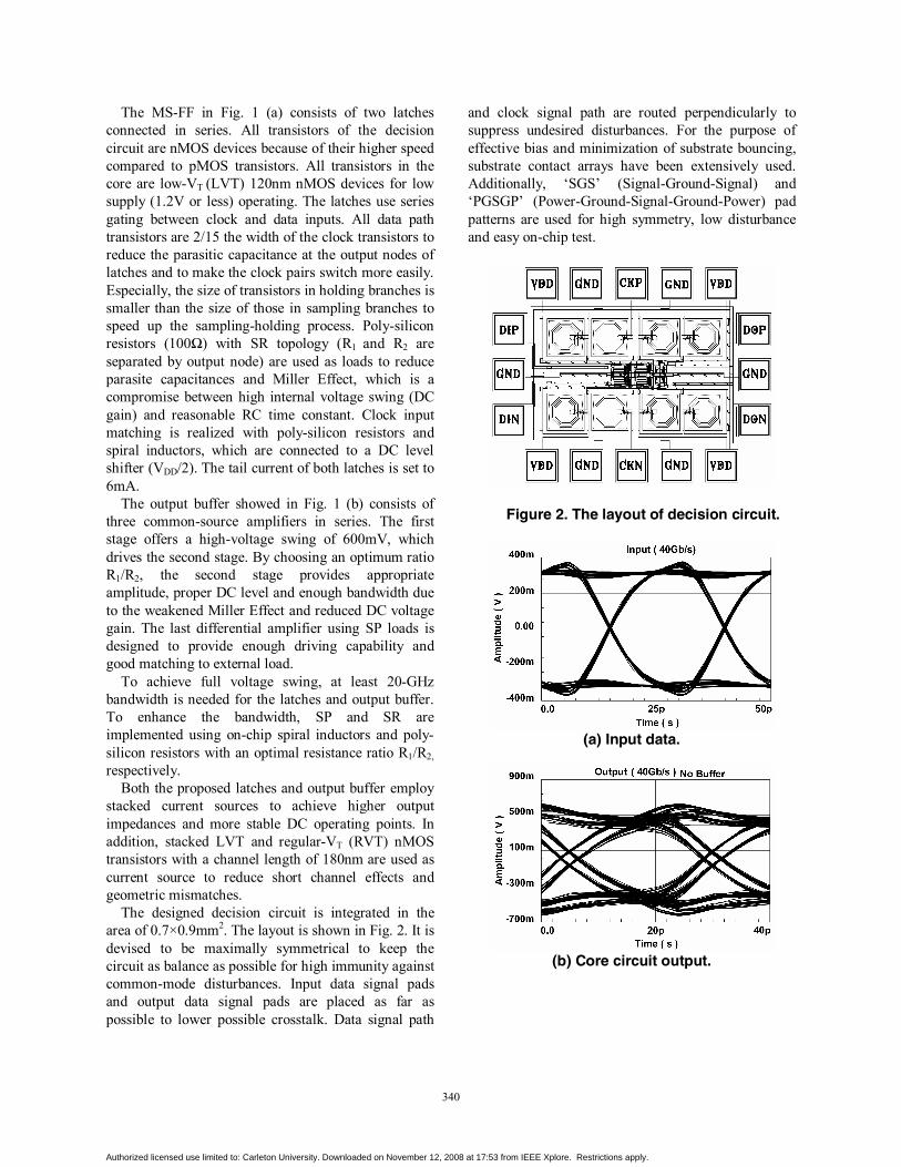
The designed decision circuit is integrated in the area of 0.7×0.9mm2. The layout is shown in Fig. 2. It is devised to be maximally symmetrical to keep the circuit as balance as possible for high immunity against common-mode disturbances. Input data signal pads and output data signal pads are placed as far as possible to lower possible crosstalk. Data signal path
and clock signal path are routed perpendicularly to suppress undesired disturbances. For the purpose of effective bias and minimization of substrate bouncing, substrate contact arrays have been extensively used. Additionally, ‘SGS’ (Signal-Ground-Signal) and ‘PGSGP’ (Power-Ground-Signal-Ground-Power) pad patterns are used for high symmetry, low disturbance and easy on-chip test.
Figure 2. The layout of decision circuit.
(a) Input data.
(b) Core circuit output.
332332334340340
Authorized licensed use limited to: Carleton University. Downloaded on November 12, 2008 at 17:53 from IEEE Xplore. Restrictions apply.
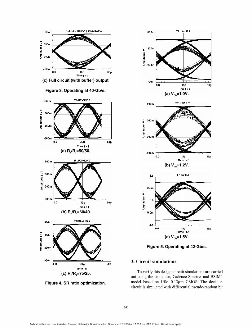
(c) Full circuit (with buffer) output
Figure 3. Operating at 40-Gb/s.
(a) R1/R2=50/50.
(b) R1/R2=60/40.
(c) R1/R2=75/25.
Figure 4. SR ratio optimization.
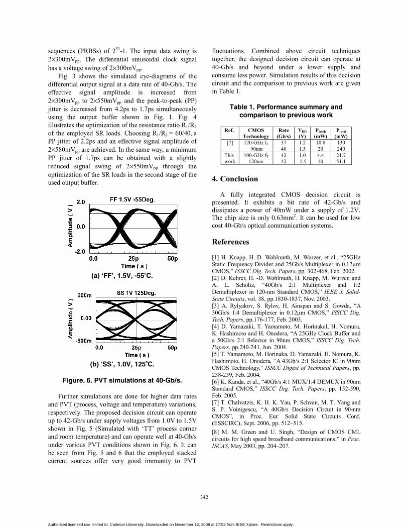
(a) VDD=1.0V.
(b) VDD=1.2V.
(c) VDD=1.5V.
Figure 5. Operating at 42-Gb/s.
3. Circuit simulations
To verify this design, circuit simulations are carried out using the simulator, Cadence Spectre, and BSIM4 model based on IBM 0.13µm CMOS. The decision circuit is simulated with differential pseudo-random bit
333333335341341
Authorized licensed use limited to: Carleton University. Downloaded on November 12, 2008 at 17:53 from IEEE Xplore. Restrictions apply.
sequences (PRBSs) of 231-1. The input data swing is 2×300mVpp. The differential sinusoidal clock signal has a voltage swing of 2×300mVpp.
Fig. 3 shows the simulated eye-diagrams of the differential output signal at a data rate of 40-Gb/s. The effective signal amplitude is increased from 2×300mVpp to 2×550mVpp and the peak-to-peak (PP) jitter is decreased from 4.2ps to 1.7ps simultaneously using the output buffer shown in Fig. 1. Fig. 4 illustrates the optimization of the resistance ratio R1/R2
of the employed SR loads. Choosing R1/R2 = 60/40, a PP jitter of 2.2ps and an effective signal amplitude of 2×580mVpp are achieved. In the same way, a minimum PP jitter of 1.7ps can be obtained with a slightly reduced signal swing of 2×550mVpp through the optimization of the SR loads in the second stage of the used output buffer.
(a) ‘FF’, 1.5V, -55oC.
(b) ‘SS’, 1.0V, 125oC.
Figure. 6. PVT simulations at 40-Gb/s.
Further simulations are done for higher data rates
and PVT (process, voltage and temperature) variations, respectively. The proposed decision circuit can operate up to 42-Gb/s under supply voltages from 1.0V to 1.5V shown in Fig. 5 (Simulated with ‘TT’ process corner and room temperature) and can operate well at 40-Gb/s under various PVT conditions shown in Fig. 6. It can be seen from Fig. 5 and 6 that the employed stacked current sources offer very good immunity to PVT
fluctuations. Combined above circuit techniques together, the designed decision circuit can operate at 40-Gb/s and beyond under a lower supply and consume less power. Simulation results of this decision circuit and the comparison to previous work are given in Table 1.
Table 1. Performance summary and comparison to previous work
Ref. CMOS
Technology Rate
(Gb/s) VDD (V)
Platch (mW)
Ptotal (mW)
[7] 120-GHz fT
90nm 37 40
1.2 1.5
10.8 20
130 240
This work
100-GHz fT 120nm
42 42
1.0 1.5
4.4 10
21.7 51.1
4. Conclusion
A fully integrated CMOS decision circuit is presented. It exhibits a bit rate of 42-Gb/s and dissipates a power of 40mW under a supply of 1.2V. The chip size is only 0.63mm2. It can be used for low cost 40-Gb/s optical communication systems. References [1] H. Knapp, H.-D. Wohlmuth, M. Wurzer, et al., “25GHz Static Frequency Divider and 25Gb/s Multiplexer in 0.12µm CMOS,” ISSCC Dig. Tech. Papers, pp. 302-468, Feb. 2002. [2] D. Kehrer, H. -D. Wohlmuth, H. Knapp, M. Wurzer, and A. L. Scholtz, “40Gb/s 2:1 Multiplexer and 1:2 Demultiplexer in 120-nm Standard CMOS,” IEEE J. Solid-State Circuits, vol. 38, pp.1830-1837, Nov. 2003. [3] A. Rylyakov, S. Rylov, H. Ainspan and S. Gowda, “A 30Gb/s 1:4 Demultiplexer in 0.12µm CMOS,” ISSCC Dig. Tech. Papers, pp.176-177, Feb. 2003. [4] D. Yamazaki, T. Yamamoto, M. Horinakal, H. Nomura, K. Hashimoto and H. Onodera, “A 25GHz Clock Buffer and a 50Gb/s 2:1 Selector in 90nm CMOS,” ISSCC Dig. Tech. Papers, pp.240-241, Jun. 2004. [5] T. Yamamoto, M. Horinaka, D. Yamazaki, H. Nomura, K. Hashimoto, H. Onodera, “A 43Gb/s 2:1 Selector IC in 90nm CMOS Technology,” ISSCC Digest of Technical Papers, pp. 238-239, Feb. 2004. [6] K. Kanda, et al., “40Gb/s 4:1 MUX/1:4 DEMUX in 90nm Standard CMOS,” ISSCC Dig. Tech. Papers, pp. 152-590, Feb. 2005. [7] T. Chalvatzis, K. H. K. Yau, P. Schvan, M. T. Yang and S. P. Voinigescu, “A 40Gb/s Decision Circuit in 90-nm CMOS”, in Proc. Eur. Solid State Circuits Conf. (ESSCIRC), Sept. 2006, pp. 512–515. [8] M. M. Green and U. Singh, “Design of CMOS CML circuits for high speed broadband communications,” in Proc. ISCAS, May 2003, pp. 204–207.
334334336342342
Authorized licensed use limited to: Carleton University. Downloaded on November 12, 2008 at 17:53 from IEEE Xplore. Restrictions apply.