3D Modeling and Simulation of Hg 2 Cl 2 Crystal Growth by Physical Vapor Transport
Linköping University Post Print
α-alumina coatings on WC/Co substrates by physical vapor deposition
T.I. Selinder, E. Coronel, Erik Wallin and Ulf Helmersson
N.B.: When citing this work, cite the original article.
Original Publication:
T.I. Selinder, E. Coronel, Erik Wallin and Ulf Helmersson, α-alumina coatings on WC/Co substrates by physical vapor deposition, 2009, International journal of refractory metals & hard materials, (27), 2, 507-512. http://dx.doi.org/10.1016/j.ijrmhm.2008.10.007 Copyright: Elsevier Science B.V., Amsterdam.
http://www.elsevier.com/
Postprint available at: Linköping University Electronic Press http://urn.kb.se/resolve?urn=urn:nbn:se:liu:diva-15359
α-ALUMINA COATINGS ON WC/Co SUBSTRATES BY PHYSICAL VAPOR
DEPOSITION
T.I. Selinder*, E. Coronel*, E. Wallin**, U. Helmersson**
*Sandvik Tooling, SE-126 80 Stockholm, Sweden
**Plasma and Coatings Physics Division, IFM Material Physics, Linköping University,
SE-581 83 Linköping, Sweden
Abstract
Physical vapor deposition coatings for cutting tools may be deposited by, e.g. reactive
magnetron sputtering. Alumina growth in Ar/O2 gas mixtures gives rise to problems due
to insulating layers on targets, and hysteresis effects with respect to oxygen gas flow. In
this paper is described a technology for the deposition of crystalline alumina: reactive
high power impulse magnetron sputtering. Pure Al was used as target material, and the
cemented carbide (WC/Co) substrates were kept at 500-650ºC. Hysteresis effects with
respect to oxygen gas flow were alleviated, which enabled stable growth at a high
deposition rate. The high power impulses were helpful in obtaining a crystalline oxide
coating. X-ray diffraction and cross-section transmission electron microscopy showed
that α-alumina films were formed. Technological testing of these PVD alumina
coatings, with state-of-the-art AlTiN as benchmark, showed significantly improved
crater wear resistance in steel turning.
Keywords: HiPIMS, HPPMS, ionized-PVD, alumina, corundum
Page 1 of 18
Introduction
Hard physical vapor deposited (PVD) coatings may be coated by a variety of methods,
e.g. direct current (DC) magnetron sputtering in Ar inert gas. Reactive sputtering in
Ar/oxygen gas mixtures, may be used to grow oxides, but for insulators, in particular
alumina, this gives rise to problems due to the formation of insulating layers.
Conducting surfaces are a prerequisite to sustain an electrical glow discharge in DC
mode. These problems are circumvented in the bipolar pulsed magnetron technique
(BPDMS) [1-2], in which two magnetrons work in pair, alternating as anode and
sputtering target. By using pulse frequencies in the range of a few kHz the Al erosion
rate exceeds the rate of oxide formation at each target surface. Albeit stable, BPDMS
has only been repeatedly successful in depositing γ-alumina, which is a drawback if
phase stability of the coating is of concern. So far, commercial α-alumina coatings have
only been grown by chemical vapor deposition (CVD) at relatively high substrate
temperatures. In order to coat heat sensitive substrates, e.g. polycrystalline c-BN, high
speed steel, brazed tools, etc. the process temperature needs to be reduced. For this and
other reasons research and development on PVD alumina by, for instance, dual
magnetron sputtering [3], and arc evaporation [4] has been intense for the past few
years. Preoxidation of Cr-containing surfaces have enabled nucleation and growth of α-
alumina [5], but still requires substrate temperatures of 700-750ºC. A commercial
technology capable of growing highly crystalline mixed oxides (Al,Cr)2O3 by the arc
method at temperatures below 600ºC were recently made available on the market [6],
but the commercialization of pure PVD α-alumina still remains. In this context the
novel technology high power impulse magnetron sputtering (HiPIMS) [7,8]have been
studied because this intermittent very high energetic sputtering technique widens the
Page 2 of 18
possibilities of supplying energy to the growth surface, which likely is the key to
success in nucleating α-alumina, and sustaining its growth. The HiPIMS technique has
been studied for deposition of both conducting coatings [9] as well as for oxide coatings
[10-11]. The degree of ionization of the sputtered material may be higher than for
traditional sputtering but the ionized species also accelerate towards the target, so-called
self sputtering, that has a lower sputtering yield than that of Ar sputtering. Therefore
one drawback with HiPIMS has been the inherently low growth rate. Recently, it was
shown that high rate sputtering is possible, and that long time stable operation of Ar/O2
discharges is possible without feedback control of the reactive gas [12]. Stoichiometric
alumina was grown, with a phase structure that was dependent on substrate temperature;
at temperatures as low as 650ºC α-alumina was the only crystalline phase detected by
X-ray diffraction (XRD). Initial transmission electron microscopy (TEM) studies
revealed, however, that γ-alumina may grow, at least during the early stages in film
growth directly on WC/Co. XRD indicates that at the same temperature and identical
growth conditions AlTiN pre-coated substrates tend to favor growth of α- over γ-
alumina. A possible origin of this difference is discussed.
Experimental details
Coatings were made in a laboratory scale ultra-high vacuum system, with a base
pressure of less than 3×10⁻⁵ Pa. A planar, 50mm diameter shuttered magnetron
sputtering source was mounted with a pure (99.999%) 3mm thick Al target. Cemented
carbide, WC10%Co (H10F), substrates were mounted flat on a resistive heater directly
above the magnetron, at a distance of 11 cm. Temperatures during different runs were
maintained at 650, 575, and 500 ºC. In order to grow films on cutting edges ISO style
Page 3 of 18
CNMG120408-MM H10F substrates were mounted, two at a time, on a tilted holder.
One nose and cutting edge was directed towards the magnetron. In this way both the
tool rake and flank faces were coated. In the latter case, however, it is estimated that the
real substrate temperature is approx. 50ºC less than the nominal set value. The
temperature reported herein is always the set nominal temperature, however, not the
estimated temperature. Substrates were either floating, or bias was applied by radio
frequency (RF) by an Advanced Energy RFX-600 power supply.
A fixed 99.997% pure Ar flow was adjusted to establish a pressure of 2.7 Pa. The
substrates were sputter etched for 15 minutes in an RF glow discharge resulting in a
-175 V DC bias of the sample holder, after which the pressure was reduced to 0.8 Pa,
and the sputtering initiated with the shutter closed. Sputtering was carried out by means
of a DC voltage source pulsed by a Melec SPIK1000A unit. The Al target was sputtered
at an average power of 110W (~5 Wcm-2) in pulses having a peak power in excess of
6kW, or 300 Wcm-2. The process working point was controlled by selecting the
99.9995% pure oxygen flow, to a value of approximately 2% of the Ar flow. The
oxygen flow was determined empirically so that transparent coatings were deposited. It
is expected that substrate oxidation during this stage is low: As the oxygen was
introduced when the discharge was running with the shutter closed it is reasonably
assumed that the partial pressure of oxygen is low in the deposition chamber; in the
working point chosen it is to a large extent consumed, incorporated in the growing film.
Also, there were no visible discolorations, after coating runs, of uncoated substrate
surfaces exposed to the sputtering atmosphere. To the extent of the analyses performed
in the present work the process was reproducible, in that consecutive runs under the
Page 4 of 18
same conditions yielded coatings with similar properties. The substrate shutter was
opened after stabilizing the process for a few minutes. The process was then able to run
stable for the duration of a typical run of at least 3 hours, without using any feedback
process control. Coatings for analyses were grown for 1h 30min., and for cutting tests
the coating time was extended to 3h 30min.
As-deposited WC/Co pieces and inserts were characterized by XRD in standard Bragg
Brentano geometry and by using Cu Kα-radiation. In order to increase the diffracted
intensity of some of the films grazing incidence XRD (GIXRD) was used with a fixed
incidence angle ω = 4º. Scanning electron microscopy (SEM) was done in a Hitachi
S4300 FEG SEM, on film surfaces and on fracture sections prepared by standard
methods. TEM cross-section samples were produced by means of classical sample
preparation by first mechanical dimpling with diamond particles and finally thinned to
electron transparency by Ar ion etching. They were then analyzed in a JEOL 2010 TEM
equipped with a LaB6 electron emitter and operated at 200kV. Bright field (BF) and
dark field (DF) imaging, and selected area electron diffraction (SAED) was performed
for microstructural characterization. Energy dispersive X-ray spectroscopy (EDS) for
chemical analysis was performed using a Link Oxford system.
On the HiPIMS Process
HiPIMS resembles ordinary magnetron sputtering in many aspects. The main difference
is the extremely high instantaneous peak power applied to the target. For this reason the
process need to be operated at very low duty factor, i.e. the power is delivered in short,
intense, packages with relatively long pauses in between. As will be described these
Page 5 of 18
high power levels, in this case around 6 kW to a target of 2” diameter (area 20 cm2)
implies some fundamental differences.
Hysteresis effects occur with respect to reactive gas flow, in this case oxygen, in all
established magnetron sputtering techniques, such as, in BPDMS [3], and, above all, in
the DC case, as exemplified by the measurement of deposition rate shown in Fig 1 a: As
oxygen is blended in the sputtering gas the deposition rate first increases, due to the
incorporation of oxygen in the growing film, to form an oxide layer. In this regime the
oxygen partial pressure is low, determined by the gettering action of the growing film.
The oxygen stoichiometry of the deposit increases with the rate of oxygen flowing into
the PVD coater. Beyond a critical point the growing coating cannot absorb more
reactive gas and the oxygen starts to react with the target erosion zone. In many cases
the sputtering yield is lower for the compound now covering the target, and the
deposition rate drops. In case of alumina the rate also drops due to an increase in the
secondary electron yield of the oxidized target surface. A substantial reduction of
oxygen flow would now be required to lower the oxygen partial pressure so as to sputter
clean the target, and return to the high deposition rate branch.
This hysteresis is well known in reactive sputtering [13], and in practice the process
often requires a feedback control, using, e g, optical plasma emission, discharge voltage,
or reactive gas partial pressure [14]. The DC process may be controlled, for a short
period, to yield stoichiometric and crystalline films provided that the oxygen flow is
above a certain value, the stoichiometry limit, indicated by a dashed line in Fig 1 a. As
the anode (e.g. chamber walls) and target surfaces get coated and rendered
Page 6 of 18
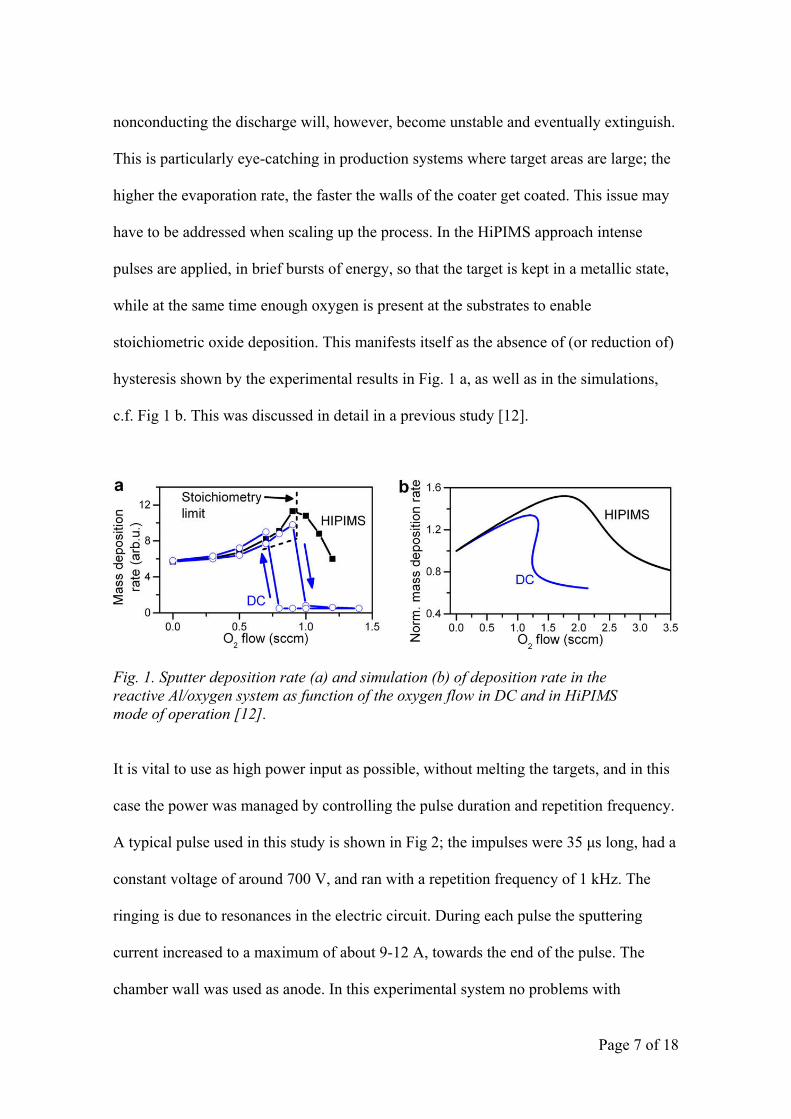
nonconducting the discharge will, however, become unstable and eventually extinguish.
This is particularly eye-catching in production systems where target areas are large; the
higher the evaporation rate, the faster the walls of the coater get coated. This issue may
have to be addressed when scaling up the process. In the HiPIMS approach intense
pulses are applied, in brief bursts of energy, so that the target is kept in a metallic state,
while at the same time enough oxygen is present at the substrates to enable
stoichiometric oxide deposition. This manifests itself as the absence of (or reduction of)
hysteresis shown by the experimental results in Fig. 1 a, as well as in the simulations,
c.f. Fig 1 b. This was discussed in detail in a previous study [12].
Fig. 1. Sputter deposition rate (a) and simulation (b) of deposition rate in the reactive Al/oxygen system as function of the oxygen flow in DC and in HiPIMS mode of operation [12].
It is vital to use as high power input as possible, without melting the targets, and in this
case the power was managed by controlling the pulse duration and repetition frequency.
A typical pulse used in this study is shown in Fig 2; the impulses were 35 μs long, had a
constant voltage of around 700 V, and ran with a repetition frequency of 1 kHz. The
ringing is due to resonances in the electric circuit. During each pulse the sputtering
current increased to a maximum of about 9-12 A, towards the end of the pulse. The
chamber wall was used as anode. In this experimental system no problems with
Page 7 of 18
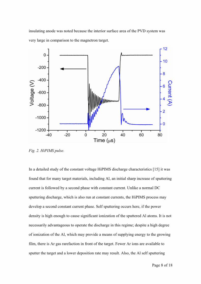
insulating anode was noted because the interior surface area of the PVD system was
very large in comparison to the magnetron target.
Fig. 2. HiPIMS pulse.
In a detailed study of the constant voltage HiPIMS discharge characteristics [15] it was
found that for many target materials, including Al, an initial sharp increase of sputtering
current is followed by a second phase with constant current. Unlike a normal DC
sputtering discharge, which is also run at constant currents, the HiPIMS process may
develop a second constant current phase. Self sputtering occurs here, if the power
density is high enough to cause significant ionization of the sputtered Al atoms. It is not
necessarily advantageous to operate the discharge in this regime; despite a high degree
of ionization of the Al, which may provide a means of supplying energy to the growing
film, there is Ar gas rarefaction in front of the target. Fewer Ar ions are available to
sputter the target and a lower deposition rate may result. Also, the Al self sputtering
Page 8 of 18
yield is less than the sputtering yield for Ar. In the present case the peak power level
was >300 Wcm-2, but the pulse time was only 35μs, so the self sputtering mode was
never entered. This was manifested in that the current maximum was reached at the e
of each pulse. It is believed that short pulses with an as high repetition frequency
possible, as allowed by target cooling efficiency, is elemental for achieving a high
deposition rate.
nd
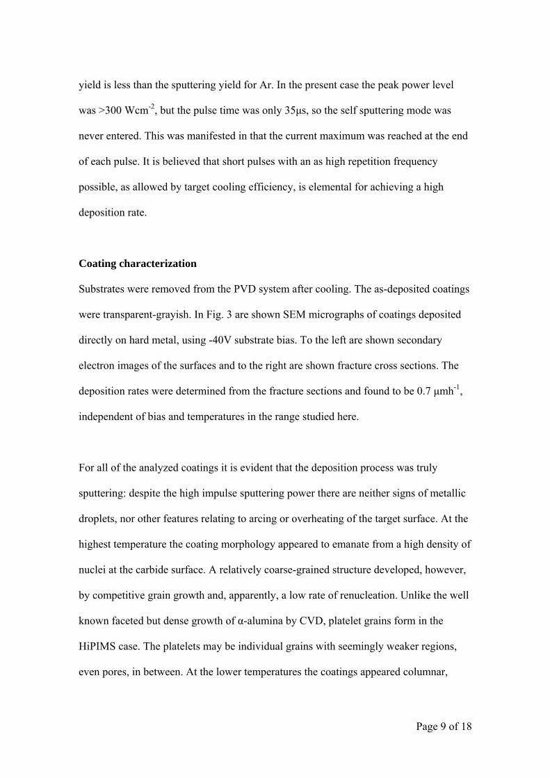
oating characterization
m the PVD system after cooling. The as-deposited coatings
he
or all of the analyzed coatings it is evident that the deposition process was truly
tallic
s,
even pores, in between. At the lower temperatures the coatings appeared columnar,
C
Substrates were removed fro
were transparent-grayish. In Fig. 3 are shown SEM micrographs of coatings deposited
directly on hard metal, using -40V substrate bias. To the left are shown secondary
electron images of the surfaces and to the right are shown fracture cross sections. T
deposition rates were determined from the fracture sections and found to be 0.7 μmh-1,
independent of bias and temperatures in the range studied here.
F
sputtering: despite the high impulse sputtering power there are neither signs of me
droplets, nor other features relating to arcing or overheating of the target surface. At the
highest temperature the coating morphology appeared to emanate from a high density of
nuclei at the carbide surface. A relatively coarse-grained structure developed, however,
by competitive grain growth and, apparently, a low rate of renucleation. Unlike the well
known faceted but dense growth of α-alumina by CVD, platelet grains form in the
HiPIMS case. The platelets may be individual grains with seemingly weaker region
Page 9 of 18
Fig. 3. Secondary electron micrographs of the surfaces of the alumina coatings (left), and cross section fracture surfaces (right). Deposition temperatures from top to bottom: 650, 575, and 500ºC.
xpected, of course, since adatom surface mobilities are lower, the lower the substrate
indicative of more uniform growth rate, and of smaller grain sizes; this is to be
e
Page 10 of 18
surface temperature is. The different morphology may also indicate a different c
structure. For this reason the coatings were further analyzed by XRD and TEM.
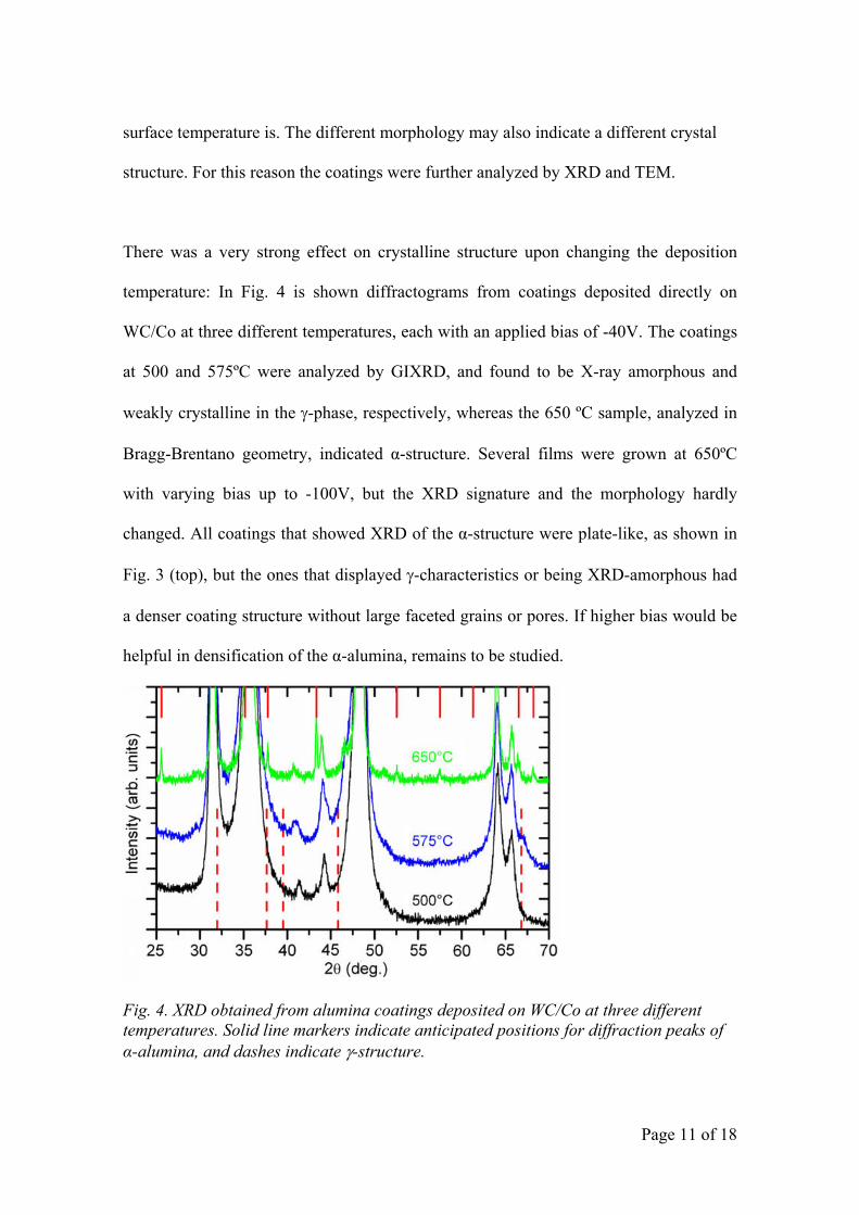
There was a very strong effect on crystalline structure upon changing the dep
rystal
osition
mperature: In Fig. 4 is shown diffractograms from coatings deposited directly on te
WC/Co at three different temperatures, each with an applied bias of -40V. The coatings
at 500 and 575ºC were analyzed by GIXRD, and found to be X-ray amorphous and
weakly crystalline in the γ-phase, respectively, whereas the 650 ºC sample, analyzed in
Bragg-Brentano geometry, indicated α-structure. Several films were grown at 650ºC
with varying bias up to -100V, but the XRD signature and the morphology hardly
changed. All coatings that showed XRD of the α-structure were plate-like, as shown in
Fig. 3 (top), but the ones that displayed γ-characteristics or being XRD-amorphous had
a denser coating structure without large faceted grains or pores. If higher bias would be
helpful in densification of the α-alumina, remains to be studied.
Fig. 4. XRD obtained from alumina coatings deposited on WC/Co at three different temperatures. Solid line markers indicate anticipated positions for diffraction peaks of α-alumina, and dashes indicate γ-structure.
Page 11 of 18
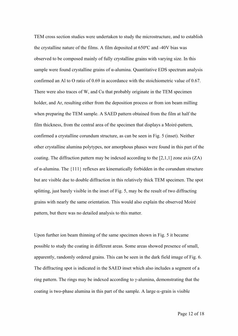
TEM cross section studies were undertaken to study the microstructure, and to establ
the crystalline nature of the films. A film dep
ish
osited at 650ºC and -40V bias was
observed to be composed mainly of fully crystalline grains with varying size. In this
sample were found crystalline grains of α-alumina. Quantitative EDS spectrum analysis
confirmed an Al to O ratio of 0.69 in accordance with the stoichiometric value of 0.67.
There were also traces of W, and Cu that probably originate in the TEM specimen
holder, and Ar, resulting either from the deposition process or from ion beam milling
when preparing the TEM sample. A SAED pattern obtained from the film at half the
film thickness, from the central area of the specimen that displays a Moiré-pattern,
confirmed a crystalline corundum structure, as can be seen in Fig. 5 (inset). Neither
other crystalline alumina polytypes, nor amorphous phases were found in this part of the
coating. The diffraction pattern may be indexed according to the [2,1,1] zone axis (ZA)
of α-alumina. The {111} reflexes are kinematically forbidden in the corundum structure
but are visible due to double diffraction in this relatively thick TEM specimen. The spot
splitting, just barely visible in the inset of Fig. 5, may be the result of two diffracting
grains with nearly the same orientation. This would also explain the observed Moiré
pattern, but there was no detailed analysis to this matter.
Upon further ion beam thinning of the same specimen shown in Fig. 5 it became
possible to study the coating in different areas. Some areas showed presence of small,
apparently, randomly ordered grains. This can be seen in the dark field image of Fig. 6.
The diffracting spot is indicated in the SAED inset which also includes a segment of a
ring pattern. The rings may be indexed according to γ-alumina, demonstrating that the
coating is two-phase alumina in this part of the sample. A large α-grain is visible
Page 12 of 18
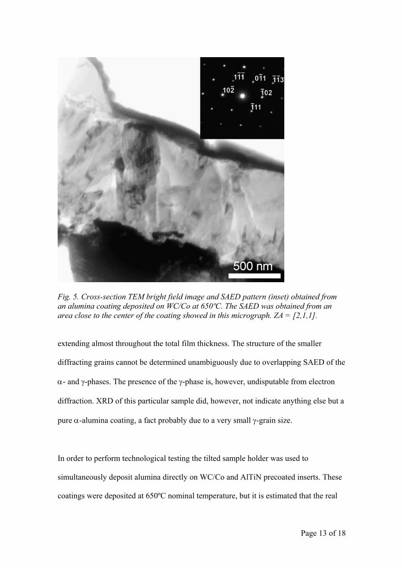
Fig. 5. Cross-section TEM bright field image and SAED pattern (inset) obtained from an alumina coating deposited on WC/Co at 650ºC. The SAED was obtained from an area close to the center of the coating showed in this micrograph. ZA = [2,1,1].
on
to
multaneously deposit alumina directly on WC/Co and AlTiN precoated inserts. These
coatings were deposited at 650ºC nominal temperature, but it is estimated that the real
extending almost throughout the total film thickness. The structure of the smaller
iffracting grains cannot be determined unambiguously due to overlapping SAED of the d
α- and γ-phases. The presence of the γ-phase is, however, undisputable from electr
diffraction. XRD of this particular sample did, however, not indicate anything else but a
pure α-alumina coating, a fact probably due to a very small γ-grain size.
In order to perform technological testing the tilted sample holder was used
si
Page 13 of 18
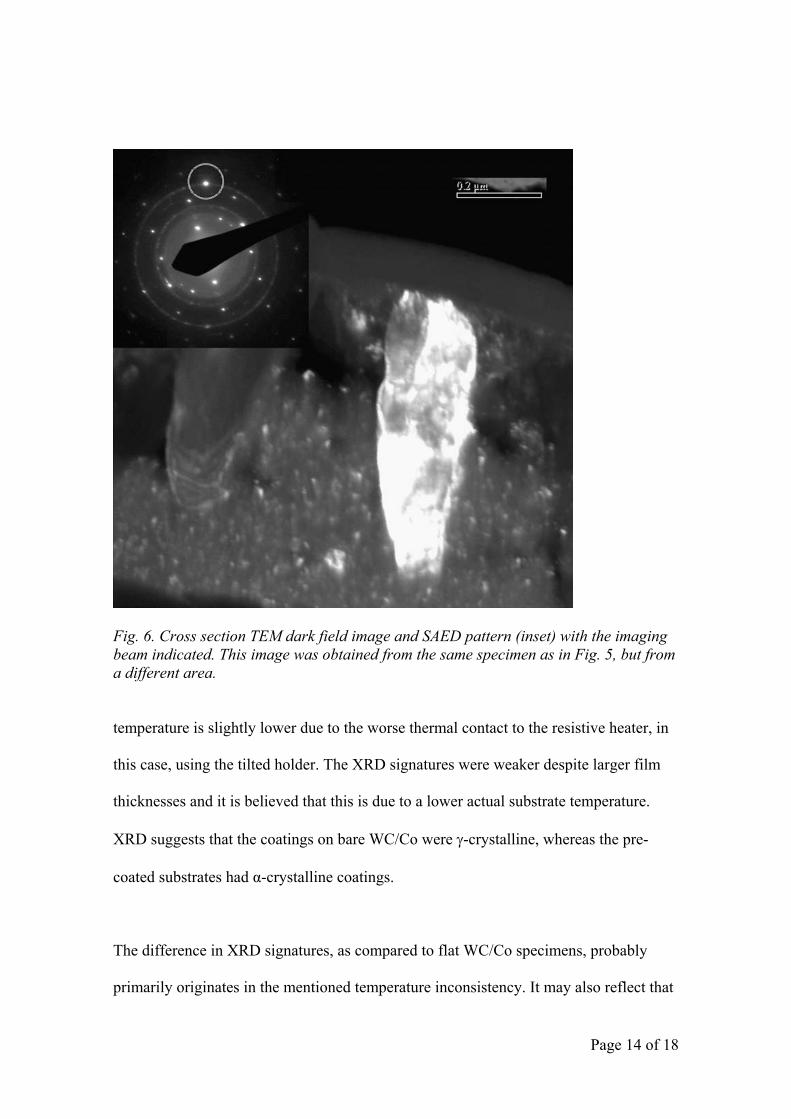
Fig. 6. Cross section TEM dark field image and SAED pattern (inset) with the imaging beam indicated. This image was obtained from the same specimen as in Fig. 5, but from a different area.
temperature is slightly lower due to the worse thermal contact to the resistive heater, in
icknesses and it is believed that this is due to a lower actual substrate temperature.
ture inconsistency. It may also reflect that
this case, using the tilted holder. The XRD signatures were weaker despite larger film
th
XRD suggests that the coatings on bare WC/Co were γ-crystalline, whereas the pre-
coated substrates had α-crystalline coatings.
The difference in XRD signatures, as compared to flat WC/Co specimens, probably
primarily originates in the mentioned tempera
Page 14 of 18
the coating time was much longer for the cutting tools than for the flat specimens. In
,
ccording to Table I. As described one useable edge was coated on each insert,
is due to
. 7
The
this case it is to be expected that mobile substrate atoms, e.g. C may diffuse into the
coating and disrupt the growth process. Detailed and further analysis of this is beyond
the scope of this paper but will be the topic of further investigations.
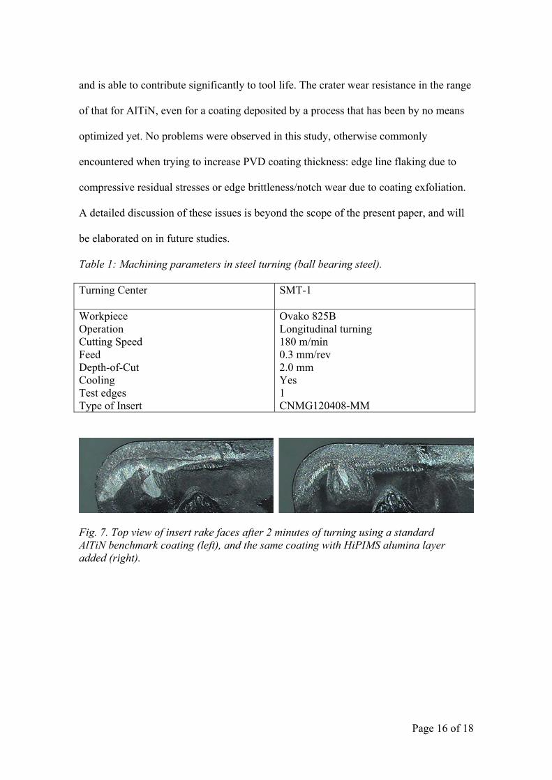
In addition to the microstructural characterization, technological testing was performed
in this case a longitudinal continuous turning test. The cutting parameters were set up
a
consequently only rudimentary studies could be performed. Since it is anticipated that
alumina will improve the chemical stability of the tool surface on which the chips flow
a test was selected that emphasizes the wear on the rake face. This type of wear
chemical dissolution of the tool material into the (steel) chip, and eventually gives rise
to a crater that extends into the substrate. The benchmark AlTiN coating had a tool life
of 4 minutes, and the alumina deposited on bare WC/Co was worse than the reference.
This may be due to insufficient adhesion of the alumina directly on WC/Co. The α-
alumina on AlTiN precoated tools, on the other hand, extended the tool life to 7
minutes, a significant improvement. The tool life was limited by crater wear in this test.
Therefore the rake faces only were observed to monitor the progression of wear. Fig
shows the extent of crater wear after 2 minutes machining time for both variants.
crater is visible as the light gray exposed WC/Co substrate of the benchmark (left),
while the crater hardly started to develop on the HiPIMS variant (right). The reference
coating has a coating thickness of approximately 2 μm and the HiPIMS alumina added
another 2μm to the other insert. Coating thicknesses could only be estimated after
turning. What is obvious from this first test is, nonetheless, that the alumina is adherent
Page 15 of 18
and is able to contribute significantly to tool life. The crater wear resistance in the range
of that for AlTiN, even for a coating deposited by a process that has been by no me
optimized yet. No problems were observed in this study, otherwise commonly
encountered when trying to increase PVD coating thickness: edge line flaking due to
compressive residual stresses or edge brittleness/notch wear due to coating exfoliation.
A detailed discussion of these issues is beyond the scope of the present paper, a
be elaborated on in future studies.
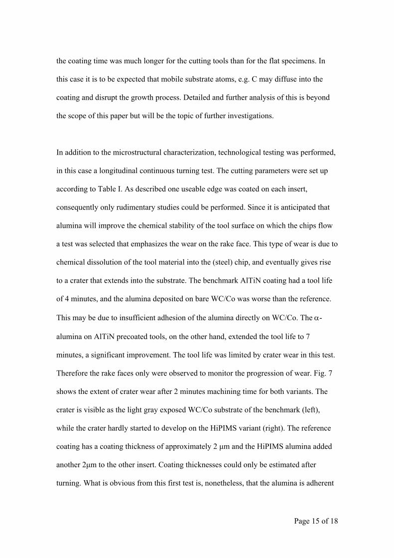
Table 1: Machining parameters in steel turning (ball bearing steel).
Turning Center SMT-1
ans
nd will
Workpiece Operation
Feed
Cooling
ert
Ovako 825B Longitudinal turning
0.3 mm/rev
Yes
Cutting Speed 180 m/min
Depth-of-Cut
Test edges Type of Ins
2.0 mm
1 CNMG120408-MM
Fig. 7. Top view of insert rake faces after 2 minutes of turning using a standard AlTiN benchmark coating (left), and the same coating with HiPIMS alumina layer added (right).
Page 16 of 18
Conclusions
In this study the HiPIMS technique was used to deposit alumina coatings on WC/Co
substrates and tools.
• α-alumina was succesfully deposited on WC/Co substrates at 650 °C.
• The deposition rate was found to be independent of substrate bias and substrate
temperature in the range of 500 to 650 °C.
• The crystalline structure depended on deposition temperature.
• α-alumina deposited on AlTiN precoated tools extended the tool life in a turning
application as compared to a tool only coated with AlTiN. Hence, these first
tests are promising in terms of the potential for using HiPIMS deposited alumina
as a wear-resistant coating in metal cutting applications.
Acknowledgements
Two authors (Wallin and Helmersson) gratefully acknowledge the Swedish Research
Council and the Swedish Foundation for Strategic Research for financial support during
the course of this work.
Page 17 of 18
Page 18 of 18
References
1. O. Zywitski, G. Hoetsch, Surf. Coat. Technol., 86-87 (1996) 640.
2. O. Zywitski, and G. Hoetsch, Surf. Coat. Technol., 94-95 (1997) 303.
3. M. Åstrand, T.I. Selinder, F. Fietzke, and H. Klostermann, Surf. Coat. Technol.,
188-189 (2004) 186.
4. Y. Yamada-Takamura, F. Koch, H. Maier, and H. Bolt, Surf. Coat. Technol.,
142-144 (2001) 260.
5. T. Kohara, H. Tamagaki, Y. Ikari, and H. Fuji, Surf. Coat. Technol., 185 (2004)
166.
6. J. Ramm, M. Ante, T. Bachmann, B. Widrig, H. Brändle, and M. Döbeli, Surf.
Coat. Technol., 202 (2007) 876.
7. V. Kouznetsov, K. Macák, J.M. Schneider, U. Helmersson, and I. Petrov, Surf.
Coat. Technol. 122 (1999) 290.
8. U. Helmersson, M. Lattemann, J. Bohlmark, A.P. Ehiasarian, and J.T.
Gudmundsson, Thin Solid Films 513 (2006) 1.
9. A.P. Ehiasarian, W.-D. Münz, L. Hultman, U. Helmersson, and I. Petrov, Surf.
Coat. Technol., 163 (2003) 267.
10. K. Sarakinos, J. Alami, and M. Wuttig, J. Phys. D: Appl. Phys., 40 (2007) 2108.
11. S. Konstantinidis, J.P. Dauchot, and M. Hecq, Thin Solid Films, 515 (2006)
1182.
12. E. Wallin and U. Helmersson, Thin Solid Films, 516 (2008) 6398.
13. S. Berg and T. Nyberg, Thin Solid Films, 476 (2005) 215.
14. W.D. Sproul, D.J. Christie, and D.C. Carter, Thin Solid Films, 491 (2005) 1.
15. A. Anders, J. Andersson, and A. Ehiasarian, J. Appl. Phys., 102 (2007) 113303