wideband transmitter Sean E. Whitehall Compact 640...
7
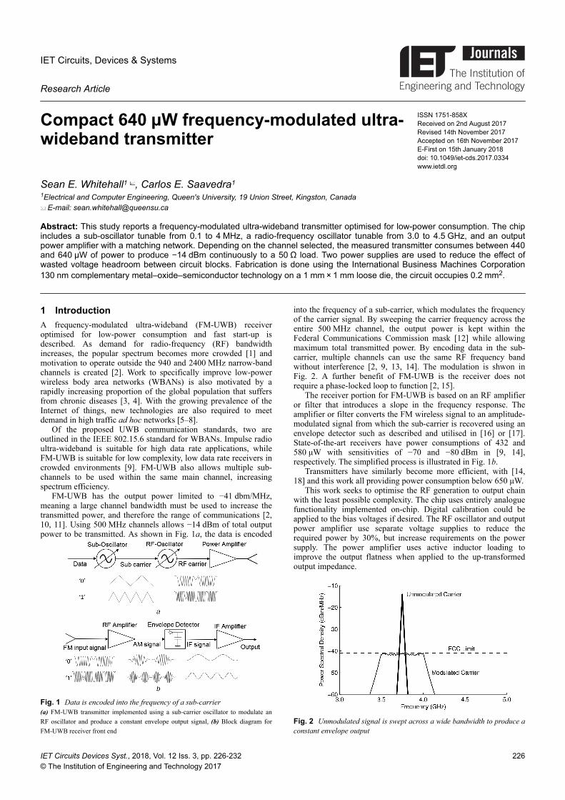
IET Circuits, Devices & Systems Research Article Compact 640 μW frequency-modulated ultra- wideband transmitter ISSN 1751-858X Received on 2nd August 2017 Revised 14th November 2017 Accepted on 16th November 2017 E-First on 15th January 2018 doi: 10.1049/iet-cds.2017.0334 www.ietdl.org Sean E. Whitehall 1 , Carlos E. Saavedra 1 1 Electrical and Computer Engineering, Queen's University, 19 Union Street, Kingston, Canada E-mail: [email protected] Abstract: This study reports a frequency-modulated ultra-wideband transmitter optimised for low-power consumption. The chip includes a sub-oscillator tunable from 0.1 to 4 MHz, a radio-frequency oscillator tunable from 3.0 to 4.5 GHz, and an output power amplifier with a matching network. Depending on the channel selected, the measured transmitter consumes between 440 and 640 μW of power to produce −14 dBm continuously to a 50 Ω load. Two power supplies are used to reduce the effect of wasted voltage headroom between circuit blocks. Fabrication is done using the International Business Machines Corporation 130 nm complementary metal–oxide–semiconductor technology on a 1 mm × 1 mm loose die, the circuit occupies 0.2 mm 2 . 1 Introduction A frequency-modulated ultra-wideband (FM-UWB) receiver optimised for low-power consumption and fast start-up is described. As demand for radio-frequency (RF) bandwidth increases, the popular spectrum becomes more crowded [1] and motivation to operate outside the 940 and 2400 MHz narrow-band channels is created [2]. Work to specifically improve low-power wireless body area networks (WBANs) is also motivated by a rapidly increasing proportion of the global population that suffers from chronic diseases [3, 4]. With the growing prevalence of the Internet of things, new technologies are also required to meet demand in high traffic ad hoc networks [5–8]. Of the proposed UWB communication standards, two are outlined in the IEEE 802.15.6 standard for WBANs. Impulse radio ultra-wideband is suitable for high data rate applications, while FM-UWB is suitable for low complexity, low data rate receivers in crowded environments [9]. FM-UWB also allows multiple sub- channels to be used within the same main channel, increasing spectrum efficiency. FM-UWB has the output power limited to −41 dbm/MHz, meaning a large channel bandwidth must be used to increase the transmitted power, and therefore the range of communications [2, 10, 11]. Using 500 MHz channels allows −14 dBm of total output power to be transmitted. As shown in Fig. 1a, the data is encoded into the frequency of a sub-carrier, which modulates the frequency of the carrier signal. By sweeping the carrier frequency across the entire 500 MHz channel, the output power is kept within the Federal Communications Commission mask [12] while allowing maximum total transmitted power. By encoding data in the sub- carrier, multiple channels can use the same RF frequency band without interference [2, 9, 13, 14]. The modulation is shwon in Fig. 2. A further benefit of FM-UWB is the receiver does not require a phase-locked loop to function [2, 15]. The receiver portion for FM-UWB is based on an RF amplifier or filter that introduces a slope in the frequency response. The amplifier or filter converts the FM wireless signal to an amplitude- modulated signal from which the sub-carrier is recovered using an envelope detector such as described and utilised in [16] or [17]. State-of-the-art receivers have power consumptions of 432 and 580 μW with sensitivities of −70 and −80 dBm in [9, 14], respectively. The simplified process is illustrated in Fig. 1b. Transmitters have similarly become more efficient, with [14, 18] and this work all providing power consumption below 650 μW. This work seeks to optimise the RF generation to output chain with the least possible complexity. The chip uses entirely analogue functionality implemented on-chip. Digital calibration could be applied to the bias voltages if desired. The RF oscillator and output power amplifier use separate voltage supplies to reduce the required power by 30%, but increase requirements on the power supply. The power amplifier uses active inductor loading to improve the output flatness when applied to the up-transformed output impedance. Fig. 1 Data is encoded into the frequency of a sub-carrier (a) FM-UWB transmitter implemented using a sub-carrier oscillator to modulate an RF oscillator and produce a constant envelope output signal, (b) Block diagram for FM-UWB receiver front end Fig. 2 Unmodulated signal is swept across a wide bandwidth to produce a constant envelope output IET Circuits Devices Syst., 2018, Vol. 12 Iss. 3, pp. 226-232 © The Institution of Engineering and Technology 2017 226
Transcript of wideband transmitter Sean E. Whitehall Compact 640...
IET Circuits, Devices & Systems
Research Article
Compact 640 μW frequency-modulated ultra-wideband transmitter
ISSN 1751-858XReceived on 2nd August 2017Revised 14th November 2017Accepted on 16th November 2017E-First on 15th January 2018doi: 10.1049/iet-cds.2017.0334www.ietdl.org
Sean E. Whitehall1 , Carlos E. Saavedra1
1Electrical and Computer Engineering, Queen's University, 19 Union Street, Kingston, Canada E-mail: [email protected]
Abstract: This study reports a frequency-modulated ultra-wideband transmitter optimised for low-power consumption. The chipincludes a sub-oscillator tunable from 0.1 to 4 MHz, a radio-frequency oscillator tunable from 3.0 to 4.5 GHz, and an outputpower amplifier with a matching network. Depending on the channel selected, the measured transmitter consumes between 440and 640 μW of power to produce −14 dBm continuously to a 50 Ω load. Two power supplies are used to reduce the effect ofwasted voltage headroom between circuit blocks. Fabrication is done using the International Business Machines Corporation130 nm complementary metal–oxide–semiconductor technology on a 1 mm × 1 mm loose die, the circuit occupies 0.2 mm2.
1 IntroductionA frequency-modulated ultra-wideband (FM-UWB) receiveroptimised for low-power consumption and fast start-up isdescribed. As demand for radio-frequency (RF) bandwidthincreases, the popular spectrum becomes more crowded [1] andmotivation to operate outside the 940 and 2400 MHz narrow-bandchannels is created [2]. Work to specifically improve low-powerwireless body area networks (WBANs) is also motivated by arapidly increasing proportion of the global population that suffersfrom chronic diseases [3, 4]. With the growing prevalence of theInternet of things, new technologies are also required to meetdemand in high traffic ad hoc networks [5–8].
Of the proposed UWB communication standards, two areoutlined in the IEEE 802.15.6 standard for WBANs. Impulse radioultra-wideband is suitable for high data rate applications, whileFM-UWB is suitable for low complexity, low data rate receivers incrowded environments [9]. FM-UWB also allows multiple sub-channels to be used within the same main channel, increasingspectrum efficiency.
FM-UWB has the output power limited to −41 dbm/MHz,meaning a large channel bandwidth must be used to increase thetransmitted power, and therefore the range of communications [2,10, 11]. Using 500 MHz channels allows −14 dBm of total outputpower to be transmitted. As shown in Fig. 1a, the data is encoded
into the frequency of a sub-carrier, which modulates the frequencyof the carrier signal. By sweeping the carrier frequency across theentire 500 MHz channel, the output power is kept within theFederal Communications Commission mask [12] while allowingmaximum total transmitted power. By encoding data in the sub-carrier, multiple channels can use the same RF frequency bandwithout interference [2, 9, 13, 14]. The modulation is shwon inFig. 2. A further benefit of FM-UWB is the receiver does notrequire a phase-locked loop to function [2, 15].
The receiver portion for FM-UWB is based on an RF amplifieror filter that introduces a slope in the frequency response. Theamplifier or filter converts the FM wireless signal to an amplitude-modulated signal from which the sub-carrier is recovered using anenvelope detector such as described and utilised in [16] or [17].State-of-the-art receivers have power consumptions of 432 and580 μW with sensitivities of −70 and −80 dBm in [9, 14],respectively. The simplified process is illustrated in Fig. 1b.
Transmitters have similarly become more efficient, with [14,18] and this work all providing power consumption below 650 μW.
This work seeks to optimise the RF generation to output chainwith the least possible complexity. The chip uses entirely analoguefunctionality implemented on-chip. Digital calibration could beapplied to the bias voltages if desired. The RF oscillator and outputpower amplifier use separate voltage supplies to reduce therequired power by 30%, but increase requirements on the powersupply. The power amplifier uses active inductor loading toimprove the output flatness when applied to the up-transformedoutput impedance.
Fig. 1 Data is encoded into the frequency of a sub-carrier(a) FM-UWB transmitter implemented using a sub-carrier oscillator to modulate anRF oscillator and produce a constant envelope output signal, (b) Block diagram forFM-UWB receiver front end
Fig. 2 Unmodulated signal is swept across a wide bandwidth to produce aconstant envelope output
IET Circuits Devices Syst., 2018, Vol. 12 Iss. 3, pp. 226-232© The Institution of Engineering and Technology 2017
226
Section 2 of this paper is the circuit design, which outlines inorder of the design of the sub-oscillator, RF oscillator, and outputpower amplifier. The circuit design is followed by themeasurement results in Section 3, which includes discussion andcomparison with state of the art. Section 4 is the conclusion, thenacknowledgements are made in Section 5.
2 Circuit design2.1 Low-frequency sub-oscillator
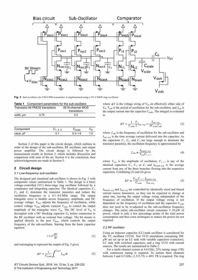
The designed and simulated sub-oscillator is shown in Fig. 3 withcomponent values summarised in Table 1. The design is a basicvoltage-controlled (VC) three-stage ring oscillator followed by acomparator and integrating capacitor. The identical capacitors C1,C2, and C3 dominate the transistor parasitics and reduce theoscillation frequency to a 0.1–4.0 MHz range. The outputtriangular wave is tunable across frequency, amplitude, and DCaverage voltage. Vbias adjusts the frequency of oscillation, whilecontrol voltage Vtune adjusts varactor Ctune to control the outputamplitude of the triangular wave Vtri. The DC level of Vtri isdecoupled with a DC blocking capacitor Cb before connection tothe RF oscillator with an external bias voltage. The bit stream isapplied directly to the port Vbias, which controls the outputfrequency of the sub-oscillator. Starting from the basic capacitorequation
i = C dVdt (1)
and rearranging to represent the output of Fig. 3 gives
ΔV = 1Cscale∫0
Tsub/2
Iout dt (2)
where ΔV is the voltage swing of Vtri on effectively either side ofCb, Tsub is the period of oscillation for the sub-oscillator, and Iout isthe output current into the capacitor Cscale. The integral is evaluatedto
ΔV = 1Cscale
T2 Iout, avg = Iout, avg
2Cscale f sub(3)
where f sub is the frequency of oscillation for the sub-oscillator andIout, avg is the time average current delivered into the capacitor. Asthe capacitors C1, C2, and C3 are large enough to dominate thetransistor parasitics, the oscillation frequency is approximated by
f sub ∝ Ibranch, avgVoscC1, 2, 3
(4)
where Vosc is the amplitude of oscillation, C1, 2, 3 is any of theidentical capacitors C1, C2, or C3 and Ibranch, avg is the averagecurrent from any of the three branches flowing into the respectivecapacitors. Combining (3) and (4) gives
ΔV ∝ VoscC1, 2, 3
Cscale
Ibranch, avgIout, avg
. (5)
Ibranch, avg and Iout, avg are controlled by identically sized and biasedcurrent source transistors, so they can be expected to change atsame rate, leaving the output voltage swing independent of thefrequency of oscillation. If the output voltage swing is notdependent on the frequency of oscillation and the capacitor Cscaledoes not need to be re-adjusted as the sub-oscillation frequencychanges. The entire sub-oscillator circuit consumes 5–10 μW ofpower, which is only a few percentage points of the total powerconsumption and thus extra techniques to reduce the power are notrequired.
2.2 RF oscillator
Using an inductor–capacitor (LC)-tank oscillator is considered forthe VC oscillator (VCO). Test VCO simulations consuming 200 μW are set up as an LC tank with variable capacitors (varactors),LC tank with switched capacitors, and a ring VCO with currentsources. The results are summarised in Table 2.
For a multi-channel system at 4.0 GHz, 25% tuning range (TR)with continuous tuning is required. To sustain three channelsbetween 3 and 4.5 GHz, (1.5/3.75) = 40% TR is required. The ring
Fig. 3 Sub-oscillator for FM-UWB transmitter is implemented using a VC CMOS ring oscillator
Table 1 Component parameters for the sub-oscillatorTransistor All PMOS transistors All N-channel MOS
transistorswidth, μm 0.75 0.3
Component C1, 2, 3 Cscale Cbvalue, pF 0.1 0.3–1.6 1.0
IET Circuits Devices Syst., 2018, Vol. 12 Iss. 3, pp. 226-232© The Institution of Engineering and Technology 2017
227
VCO is the only architecture that meets these requirements. Whilethe phase noise of the ring VCO is substantially worst, −70 versus−100 dBc/Hz at 1 MHz offset, FM-UWB systems can tolerate upto −60 dBc/Hz [2, 10, 14]. The ring VCO has the added advantageof requiring less than a tenth of the die area by eliminating the needfor an inductor.
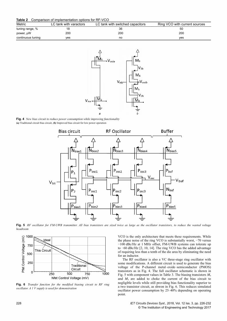
The RF oscillator is also a VC three-stage ring oscillator withsome modifications. A different circuit is used to generate the biasvoltage of the P-channel metal–oxide–semiconductor (PMOS)transistors as in Fig. 4. The full oscillator schematic is shown inFig. 5 with component values in Table 3. The biasing transistors M4and M5 are added to choke the current of the bias circuit tonegligible levels while still providing bias functionality superior toa two transistor circuit, as shwon in Fig. 6. This reduces simulatedoscillator power consumption by 25–40% depending on operatingpoint.
Table 2 Comparison of implementation options for RF-VCOMetric LC tank with varactors LC tank with switched capacitors Ring VCO with current sourcestuning range, % 18 36 50power, μW 200 200 200continuous tuning yes no yes
Fig. 4 New bias circuit to reduce power consumption while improving functionality(a) Traditional circuit bias circuit, (b) Improved bias circuit for low power operation
Fig. 5 RF oscillator for FM-UWB transmitter. All bias transistors are sized twice as large as the oscillator transistors, to reduce the wasted voltageheadroom
Fig. 6 Transfer function for the modified biasing circuit to RF ringoscillator. A 1 V supply is used for demonstration
228 IET Circuits Devices Syst., 2018, Vol. 12 Iss. 3, pp. 226-232© The Institution of Engineering and Technology 2017
To analyse the circuit in Fig. 4b in the sub-threshold regime,consider the case where the Nfet control voltage Vinb is a lowvalue. In this case, M3 can be considered ‘ON’ and the voltageVoutb is equal to VDD. The current through each transistor M4, M5,and M6 is approximated by the sub-threshold equation
IDD ≃ Id0eVfb/VT (6)
where VT = nkT /q with 1 < n < 2, k is Boltzmann's constant, T isthe temperature in Kelvin, q is the elementary charge, and Vfb is theforward-bias voltage (V1b − Voutb) for M4, (Voutb − V2b) for M5, and(Vinb − 0) for M6. The transistors M4 − 6 are sized so the voltage dropacross each is approximately the same
V1b − Voutb = VDD − Voutb = Voutb − V2b = Vinb . (7)
The important conclusion is Vinb = VDD − Voutb, giving a linearnegative relationship between the input and output. For the casewhen the Nfet control voltage Vinb is high, a similar analysis isused. The bottom transistor M6 is ‘ON’ while
VDD − Vinb = V1b − Voutb = Voutb − V2b = Voutb . (8)
or simply Voutb = VDD − Vinb as before. The final case comes whenthe Nfet control voltage Vin is in a middle range, able to turn onboth M3 and M6, whereas M4 and M5 remain in the sub-thresholdregion. For Vin2 = VDD/2, the top and bottom halves of the circuitare identical and result in Vout2 = Vin2 = VDD/2. The Pfets M4 andM5 apply negative feedback to keep the response linear until Vinreaches either of the two previous conditions, yieldingVout2 = VDD − Vin2 for all ranges of Vin. For the circuit to functionin the sub-threshold regime under higher voltages, M4 and M5 canbe each replaced with two transistors without changingfunctionality.
The frequency of oscillation is increased using forward bodybias (not shown in schematic) to reduce the threshold voltage of alltransistors.
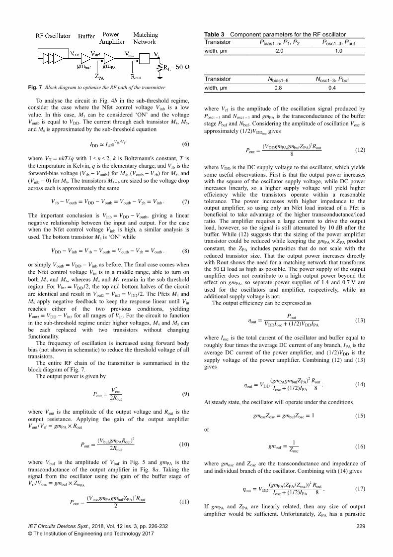
The entire RF chain of the transmitter is summarised in theblock diagram of Fig. 7.
The output power is given by
Pout = Vout2
2Rout(9)
where Vout is the amplitude of the output voltage and Rout is theoutput resistance. Applying the gain of the output amplifierVout/Vrf = gmPA × Rout
Pout = (VbufgmPARout)2
2Rout(10)
where Vbuf is the amplitude of Vbuf in Fig. 5 and gmPA is thetransconductance of the output amplifier in Fig. 8a. Taking thesignal from the oscillator using the gain of the buffer stage ofVrf /Vosc = gmbuf × ZinPA
Pout = (VoscgmPAgmbufZPA)2Rout2 (11)
where Vrf is the amplitude of the oscillation signal produced byPosc1 − 3 and Nosc1 − 3 and gmPA is the transconductance of the bufferstage Pbuf and Nbuf. Considering the amplitude of oscillation Vosc isapproximately (1/2)VDDosc gives
Pout = (VDDgmPAgmbufZPA)2Rout8 (12)
where VDD is the DC supply voltage to the oscillator, which yieldssome useful observations. First is that the output power increaseswith the square of the oscillator supply voltage, while DC powerincreases linearly, so a higher supply voltage will yield higherefficiency while the transistors operate within a reasonabletolerance. The power increases with higher impedance to theoutput amplifier, so using only an Nfet load instead of a Pfet isbeneficial to take advantage of the higher transconductance/loadratio. The amplifier requires a large current to drive the outputload, however, so the signal is still attenuated by 10 dB after thebuffer. While (12) suggests that the sizing of the power amplifiertransistor could be reduced while keeping the gmPA × ZPA productconstant, the ZPA includes parasitics that do not scale with thereduced transistor size. That the output power increases directlywith Rout shows the need for a matching network that transformsthe 50 Ω load as high as possible. The power supply of the outputamplifier does not contribute to a high output power beyond theeffect on gmPA, so separate power supplies of 1.4 and 0.7 V areused for the oscillators and amplifier, respectively, while anadditional supply voltage is not.
The output efficiency can be expressed as
ηout = PoutVDDIosc + (1/2)VDDIPA
(13)
where Iosc is the total current of the oscillator and buffer equal toroughly four times the average DC current of any branch, IPA is theaverage DC current of the power amplifier, and (1/2)VDD is thesupply voltage of the power amplifier. Combining (12) and (13)gives
ηout = VDD(gmPAgmbufZPA)2
Iosc + (1/2)IPA
Rout8 . (14)
At steady state, the oscillator will operate under the conditions
gmoscZosc = gmbufZosc = 1 (15)
or
gmbuf = 1Zosc
(16)
where gmosc and Zosc are the transconductance and impedance ofand individual branch of the oscillator. Combining with (14) gives
ηout = VDD(gmPA(ZPA/Zosc))2
Iosc + (1/2)IPA
Rout8 . (17)
If gmPA and ZPA are linearly related, then any size of outputamplifier would be sufficient. Unfortunately, ZPA has a parasitic
Table 3 Component parameters for the RF oscillatorTransistor Pbias1–5, P1, P2 Posc1–3, Pbufwidth, μm 2.0 1.0
Transistor Nbias1–5 Nosc1–3, Pbufwidth, μm 0.8 0.4
Fig. 7 Block diagram to optimise the RF path of the transmitter
IET Circuits Devices Syst., 2018, Vol. 12 Iss. 3, pp. 226-232© The Institution of Engineering and Technology 2017
229
component from the layout which increases the minimum sizing ofthe power amplifier. It can be shown that without layout parasiticsconsidered, extra stages do not contribute to the gain because everylinear increase in transconductance and capacitive loading withtransistor width simply cancel each other out. With layoutparasitics considered, any extra stages add to these parasitics andreduce the gain, motivating as few stages as possible in the RFchain.
The RF oscillator circuit is designed to consumer around 200 μA of power and the simulated phase noise is −70 dBc/Hz at 1 MHz offset when running at 4 GHz. This is well within the −60 dBc/Hz for proper operation recommended in [2, 10, 14, 19]. Thetotal power budget includes 250 μA for the power amplifier andcomes to <500 μA.
2.3 Power amplifier
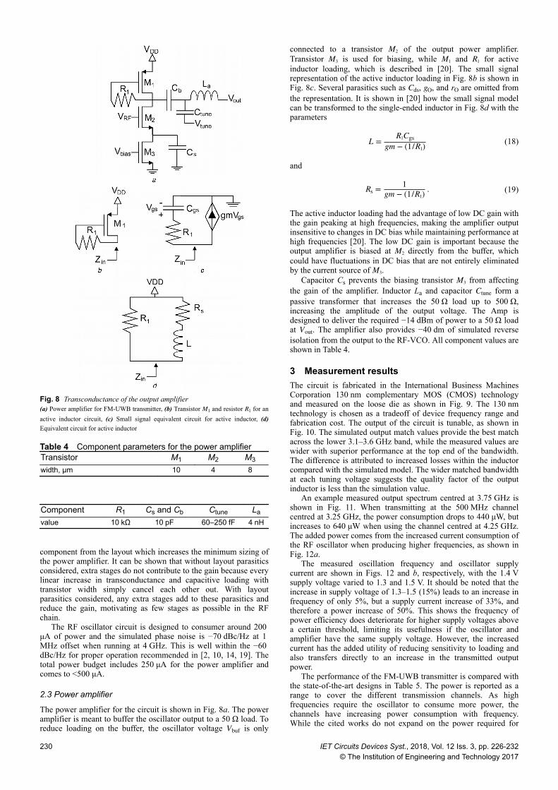
The power amplifier for the circuit is shown in Fig. 8a. The poweramplifier is meant to buffer the oscillator output to a 50 Ω load. Toreduce loading on the buffer, the oscillator voltage Vbuf is only
connected to a transistor M2 of the output power amplifier.Transistor M3 is used for biasing, while M1 and R1 for activeinductor loading, which is described in [20]. The small signalrepresentation of the active inductor loading in Fig. 8b is shown inFig. 8c. Several parasitics such as Cds, gO, and rO are omitted fromthe representation. It is shown in [20] how the small signal modelcan be transformed to the single-ended inductor in Fig. 8d with theparameters
L = R1Cgsgm − (1/R1) (18)
and
Rs = 1gm − (1/R1) . (19)
The active inductor loading had the advantage of low DC gain withthe gain peaking at high frequencies, making the amplifier outputinsensitive to changes in DC bias while maintaining performance athigh frequencies [20]. The low DC gain is important because theoutput amplifier is biased at M2 directly from the buffer, whichcould have fluctuations in DC bias that are not entirely eliminatedby the current source of M3.
Capacitor Cs prevents the biasing transistor M3 from affectingthe gain of the amplifier. Inductor La and capacitor Ctune form apassive transformer that increases the 50 Ω load up to 500 Ω,increasing the amplitude of the output voltage. The Amp isdesigned to deliver the required −14 dBm of power to a 50 Ω loadat Vout. The amplifier also provides −40 dm of simulated reverseisolation from the output to the RF-VCO. All component values areshown in Table 4.
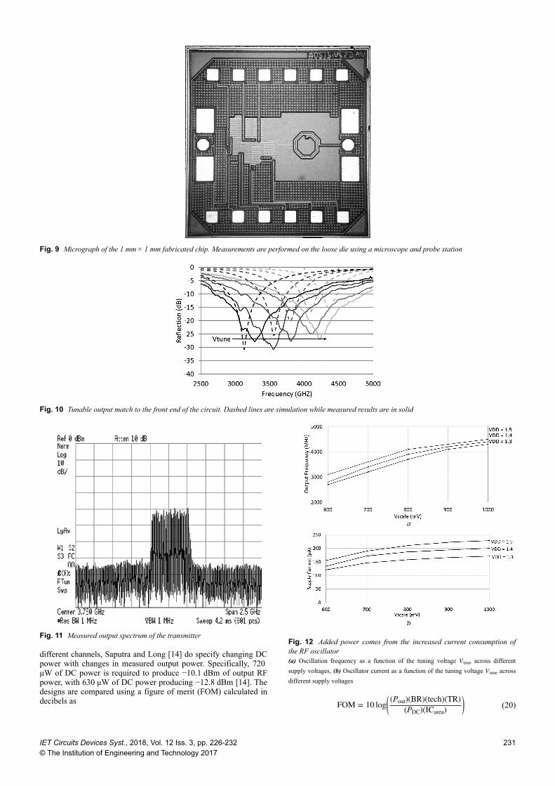
3 Measurement resultsThe circuit is fabricated in the International Business MachinesCorporation 130 nm complementary MOS (CMOS) technologyand measured on the loose die as shown in Fig. 9. The 130 nmtechnology is chosen as a tradeoff of device frequency range andfabrication cost. The output of the circuit is tunable, as shown inFig. 10. The simulated output match values provide the best matchacross the lower 3.1–3.6 GHz band, while the measured values arewider with superior performance at the top end of the bandwidth.The difference is attributed to increased losses within the inductorcompared with the simulated model. The wider matched bandwidthat each tuning voltage suggests the quality factor of the outputinductor is less than the simulation value.
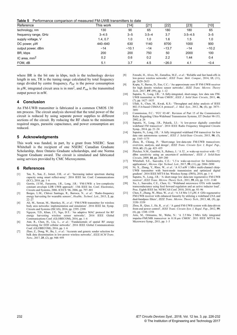
An example measured output spectrum centred at 3.75 GHz isshown in Fig. 11. When transmitting at the 500 MHz channelcentred at 3.25 GHz, the power consumption drops to 440 μW, butincreases to 640 μW when using the channel centred at 4.25 GHz.The added power comes from the increased current consumption ofthe RF oscillator when producing higher frequencies, as shown inFig. 12a.
The measured oscillation frequency and oscillator supplycurrent are shown in Figs. 12 and b, respectively, with the 1.4 Vsupply voltage varied to 1.3 and 1.5 V. It should be noted that theincrease in supply voltage of 1.3–1.5 (15%) leads to an increase infrequency of only 5%, but a supply current increase of 33%, andtherefore a power increase of 50%. This shows the frequency ofpower efficiency does deteriorate for higher supply voltages abovea certain threshold, limiting its usefulness if the oscillator andamplifier have the same supply voltage. However, the increasedcurrent has the added utility of reducing sensitivity to loading andalso transfers directly to an increase in the transmitted outputpower.
The performance of the FM-UWB transmitter is compared withthe state-of-the-art designs in Table 5. The power is reported as arange to cover the different transmission channels. As highfrequencies require the oscillator to consume more power, thechannels have increasing power consumption with frequency.While the cited works do not expand on the power required for
Fig. 8 Transconductance of the output amplifier(a) Power amplifier for FM-UWB transmitter, (b) Transistor M1 and resistor R1 for anactive inductor circuit, (c) Small signal equivalent circuit for active inductor, (d)Equivalent circuit for active inductor
Table 4 Component parameters for the power amplifierTransistor M1 M2 M3width, μm 10 4 8
Component R1 Cs and Cb Ctune Lavalue 10 kΩ 10 pF 60–250 fF 4 nH
230 IET Circuits Devices Syst., 2018, Vol. 12 Iss. 3, pp. 226-232© The Institution of Engineering and Technology 2017
different channels, Saputra and Long [14] do specify changing DCpower with changes in measured output power. Specifically, 720 μW of DC power is required to produce −10.1 dBm of output RFpower, with 630 μW of DC power producing −12.8 dBm [14]. Thedesigns are compared using a figure of merit (FOM) calculated indecibels as FOM = 10 log (Pout)(BR)(tech)(TR)
(PDC)(ICarea) (20)
Fig. 9 Micrograph of the 1 mm × 1 mm fabricated chip. Measurements are performed on the loose die using a microscope and probe station
Fig. 10 Tunable output match to the front end of the circuit. Dashed lines are simulation while measured results are in solid
Fig. 11 Measured output spectrum of the transmitter Fig. 12 Added power comes from the increased current consumption of
the RF oscillator(a) Oscillation frequency as a function of the tuning voltage Vtune across differentsupply voltages, (b) Oscillator current as a function of the tuning voltage Vtune acrossdifferent supply voltages
IET Circuits Devices Syst., 2018, Vol. 12 Iss. 3, pp. 226-232© The Institution of Engineering and Technology 2017
231
where BR is the bit rate in kbps, tech is the technology devicelength in nm, TR is the tuning range calculated by total frequencyrange divided by centre frequency, PDC is the power consumptionin μW, integrated circuit area is in mm2, and Pout is the transmittedoutput power in mW.
4 ConclusionAn FM-UWB transmitter is fabricated in a common CMOS 130 nm process. The circuit analysis showed that the total power of thecircuit is reduced by using separate power supplies to differentsections of the circuit. By reducing the RF chain to the minimumrequired stages, parasitic capacitance, and power consumption arereduced.
5 AcknowledgmentsThis work was funded, in part, by a grant from NSERC. SeanWhitehall is the recipient of one NSERC Canadian GraduateScholarship, three Ontario Graduate scholarships, and one NormaNugent Graduate award. The circuit is simulated and fabricatedusing services provided by CMC Microsystems.
6 References[1] Tan, X., Sun, Z., Jornet, J.M., et al.: ‘Increasing indoor spectrum sharing
capacity using smart reflect-array’. 2016 IEEE Int. Conf. Communications(ICC), 2016, pp. 1–6
[2] Gerrits, J.F.M., Farserotu, J.R., Long, J.R.: ‘FM-UWB: a low-complexityconstant envelope LDR UWB approach’. 13th IEEE Int. Conf. Electronics,Circuits and Systems, 2006. ICECS ‘06, 2006, pp. 797–801
[3] Borges, L.M., Chãvez Santiago, R., Barroca, N., et al.: ‘Radio-frequencyenergy harvesting for wearable sensors’, Healthc. Technol. Lett., 2015, 2, pp.22–27
[4] Ali, M., Sawan, M., Shawkey, H., et al.: ‘FM-UWB transmitter for wirelessbody area networks: implementation and simulation’. 2016 IEEE Int. Symp.Circuits and Systems (ISCAS), 2016, pp. 2395–2398
[5] Nguyen, T.D., Khan, J.Y., Ngo, D.T.: ‘An adaptive MAC protocol for RFenergy harvesting wireless sensor networks’. 2016 IEEE GlobalCommunications Conf. (GLOBECOM), 2016, pp. 1–6
[6] Atat, R., Chen, H., Liu, L., et al.: ‘Fundamentals of spatial RF energyharvesting for D2D cellular networks’. 2016 IEEE Global CommunicationsConf. (GLOBECOM), 2016, pp. 1–6
[7] Zhao, Z., Dong, W., Bu, J., et al.: ‘Accurate and generic sender selection forbulk data dissemination in low-power wireless networks’, IEEE/ACM Trans.Netw., 2017, 25, (2), pp. 948–959
[8] Fotouhi, H., Alves, M., Zamalloa, M.Z., et al.: ‘Reliable and fast hand-offs inlow-power wireless networks’, IEEE Trans. Mob. Comput., 2014, 13, (11),pp. 2620–2633
[9] Kopta, V., Barras, D., Enz, C.C.: ‘An approximate zero IF FM-UWB receiverfor high density wireless sensor networks’, IEEE Trans. Microw. TheoryTech., 2017, PP, (99), pp. 1–12
[10] Saputra, N., Long, J.R.: ‘A fully-integrated, short-range, low data rate FM-UWB transmitter in 90 nm CMOS’, IEEE J. Solid State Circuits, 2011, 46,(7), pp. 1627–1635
[11] Ullah, S., Chen, M., Kwak, K.S.: ‘Throughput and delay analysis of IEEE802.15.6-based CSMA/CA protocol’, J. Med. Syst., 2012, 36, (6), pp. 3875–3891
[12] Commission, F.C.: ‘FCC 02-48’. Revision of Part 15 of the Commission'sRules Regarding Ultra-Wideband Transmission Systems, ET Docket 98-153,2002, p. 26
[13] Saputra, N., Long, J.R., Pekarik, J.J.: ‘A low-power digitally controlledwideband FM transceiver’. 2014 IEEE Radio Frequency Integrated CircuitsSymp., 2014, pp. 21–24
[14] Saputra, N., Long, J.R.: ‘A fully integrated wideband FM transceiver for lowdata rate autonomous systems’, IEEE J. Solid-State Circuits, 2015, 50, (5),pp. 1165–1175
[15] Zhou, B., Chiang, P.: ‘Short-range low-data-rate FM-UWB transceivers:overview, analysis, and design’, IEEE Trans. Circuits Syst. I, Regul. Pap.,2016, 63, (3), pp. 423–435
[16] Pletcher, N.M., Gambini, S., Rabaey, J.: ‘A 52 _w wake-up receiver with −72 dBm sensitivity using an uncertain-if architecture’, IEEE J. Solid-StateCircuits, 2009, 44, pp. 269–280
[17] Whitehall, S.E., Saavedra, C.E.: ‘1.5 w wake-up-receiver for biotelemetryapplications’, Microw. Opt. Technol. Lett., 2017, 59, (11), pp. 2884–2890
[18] Ni, X., Zhang, Y., Rhee, W., et al.: ‘A 0.5 mW 1 Mb/s multi-channel chirp-UWB transmitter with burst-mode transmission and optimized digitalgradient’. 2016 IEEE MTT-S Int. Wireless Symp. (IWS), 2016, pp. 1–4
[19] Saputra, N., Long, J.R.: ‘A short-range low data-rate regenerative FM-UWBreceiver’, IEEE Trans. Microw. Theory Tech., 2011, 59, (4), pp. 1131–1140
[20] Xu, J., Saavedra, C.E., Chen, G.: ‘Wideband microwave OTA with tunabletransconductance using feed forward regulation and an active inductor load’.Proc. Eighth IEEE Int. NEWCAS Conf. 2010, 2010, pp. 93–96
[21] Chen, F., Zhang, W., Rhee, W., et al.: ‘A 3.8 Mw 3.5 μW; 4 GHz regenerativeFM-UWB receiver with enhanced linearity by utilizing a wideband LNA anddual-bandpass filters’, IEEE Trans. Microw. Theory Tech., 2013, 61, (9), pp.3350–3359
[22] Zhou, B., Qiao, J., He, R., et al.: ‘A gated FM-UWB system with data-drivenfront-end power control’, IEEE Trans. Circuits Syst. I, Regul. Pap., 2012, 59,(6), pp. 1348–1358
[23] Anis, M., Ortmanns, M., Wehn, N.: ‘A 2.5 Mw 2 Mb/s fully integratedimpulse-FMUMB transceiver in 0.18 μm CMOS’. 2011 IEEE MTT-S Int.Microwave Symp., 2011, pp. 1–3
Table 5 Performance comparison of measured FM-UWB transmitters to dateReference This work [14] [21] [22] [23] [10]technology, nm 130 90 65 180 180 65frequency range, GHz 3–4.5 3–5 3.5–4 3.7 3.5–4.5 3–5supply voltage, V 1.4, 0.7 1.0 1.0 1.6 1.5 1.0DC power, μW 440–640 630 1140 8700 1000 900output power, dBm −14 −10.1 −14 −13.7 −14 −10.2BR, kbps 200 200 750 50 2000 100
IC area, mm2 0.2 0.6 0.2 2.2 1.44 0.4
FOM, dB 5.1 3.7 4.5 −26.0 4.1 −0.4
232 IET Circuits Devices Syst., 2018, Vol. 12 Iss. 3, pp. 226-232© The Institution of Engineering and Technology 2017