Probe Pin Wideband Electrical Circuit Model - SWTest.org€¦ · Probe Pin Wideband Electrical...
31
Probe Pin Wideband Electrical Circuit Model Mohamed Eldessouki SV TCL – An SV Probe Company
Transcript of Probe Pin Wideband Electrical Circuit Model - SWTest.org€¦ · Probe Pin Wideband Electrical...
Probe Pin Wideband Electrical Circuit Model
Mohamed EldessoukiSV TCL – An SV Probe Company
OverviewMotivation and Objective
Introduction
Closed Form Circuit Model
Probe Pin Measurements and Simulation
Probe Pin Modeling and Verification
Summary and Conclusion
2Mohamed Eldessouki
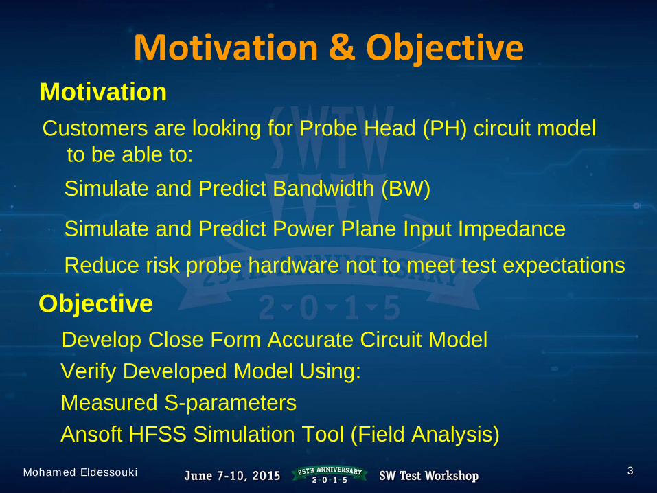
Motivation & Objective
3Mohamed Eldessouki
MotivationCustomers are looking for Probe Head (PH) circuit model
to be able to:
Objective
Simulate and Predict Bandwidth (BW)
Simulate and Predict Power Plane Input Impedance
Develop Close Form Accurate Circuit ModelVerify Developed Model Using:Measured S-parameters Ansoft HFSS Simulation Tool (Field Analysis)
Reduce risk probe hardware not to meet test expectations
Introduction
4Mohamed Eldessouki
Trio Probe & Spring Pin
Transmission Line (TL) Model
Proximity and Skin Effect
Circuit Model Comparison
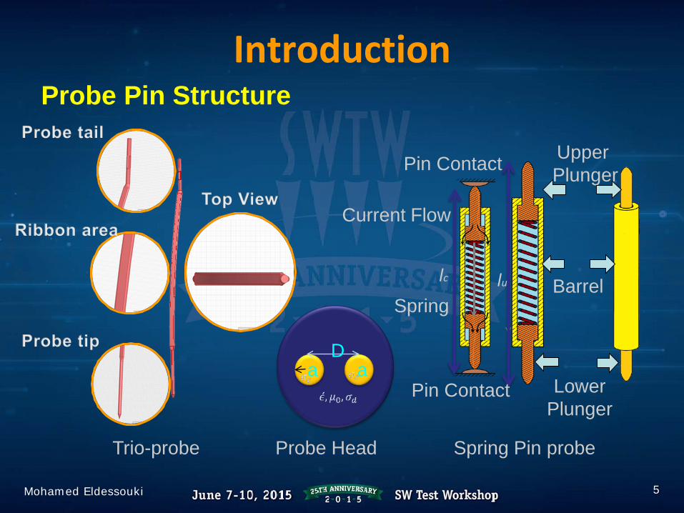
Introduction
5Mohamed Eldessouki
Probe Pin Structure
Upper Plunger
Barrel
Lower Plunger
Springlulc
Current Flow
Pin Contact
Pin Contacta a
D
Probe HeadTrio-probe Spring Pin probe
Introduction
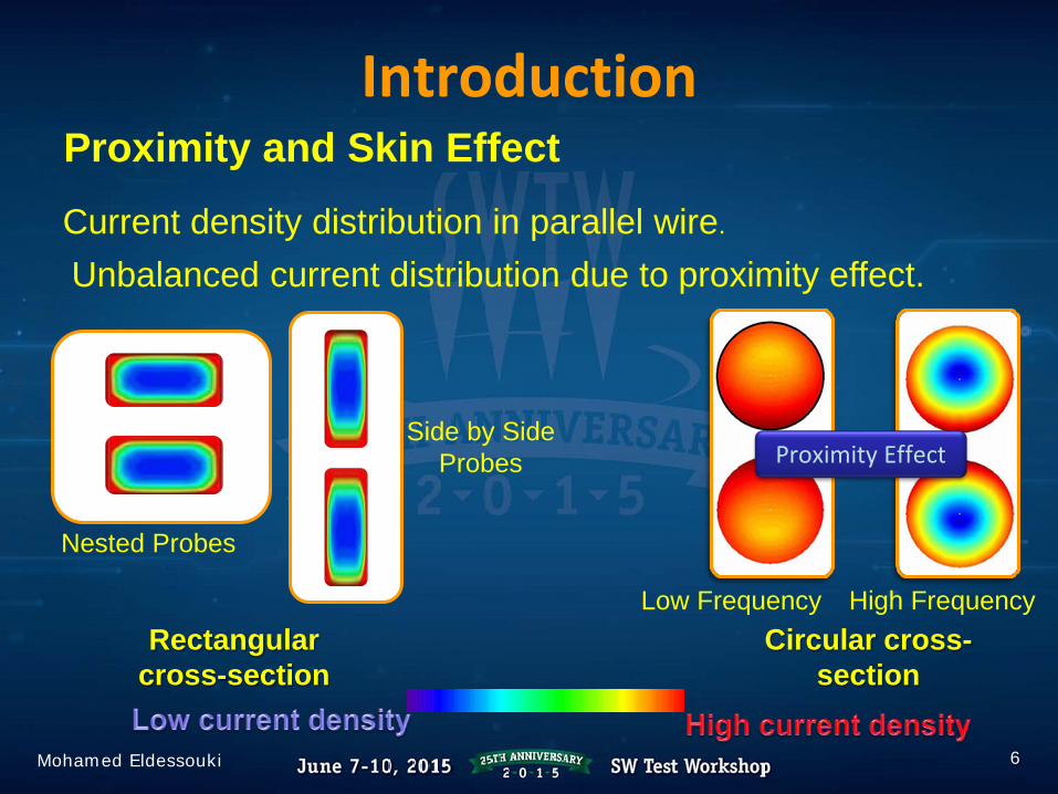
6Mohamed Eldessouki
Proximity and Skin EffectCurrent density distribution in parallel wire.
Low Frequency High Frequency
Unbalanced current distribution due to proximity effect.
Proximity Effect
Nested Probes
Side by Side Probes
Rectangular cross-section
Circular cross-section
Introduction
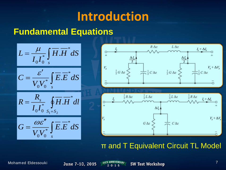
7Mohamed Eldessouki
Fundamental Equations
dSHHII
Ls
*
*00
.∫=µ
dSEEVV
Cs
*
*00
.∫′
=ε
∫+
=21
*
*00
.SS
s dlHHII
RR
dSEEVV
Gs
*
*00
.∫′′
=εω
π and T Equivalent Circuit TL Model
Introduction
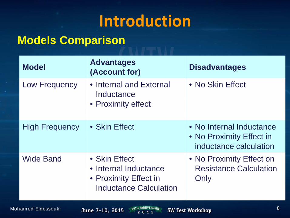
8Mohamed Eldessouki
Models Comparison
Model Advantages(Account for) Disadvantages
Low Frequency • Internal and External Inductance
• Proximity effect
• No Skin Effect
High Frequency • Skin Effect • No Internal Inductance• No Proximity Effect in
inductance calculationWide Band • Skin Effect
• Internal Inductance• Proximity Effect in
Inductance Calculation
• No Proximity Effect on Resistance Calculation Only
Closed Form Circuit Model
9Mohamed Eldessouki
Models Comparison for Cylindrical Probe
+= −
aDL2
cosh41 10
πµ
caR
σπ 22
=
= −
aDLext 2
cosh 10
πµ
( ) 12
22 −
=aD
aDa
RR s
π High Frequency
( ) ( )( ) ( )ζζ
ζζπ rjbeibe
jbeibera
RZ s
′−′+
=2int
extLjZZ ω+= int2Where
( ) ( ) ( ) ( )( )[ ] ( )[ ]( )222 ζζ
ζζζζπ rbeibe
rbejbeiibebera
RR s
′+′′−′
=
( ) ( ) ( ) ( )( )[ ] ( )[ ]( )
+
′+′′−′
= −
aD
rbeibeibejbeirbeber
aRL s
2cosh
210
22 πµ
ζζωζζζζ
π
)Re(ZR =)Im(ZL =
Low Frequency
Wide Band
Closed Form Circuit Model
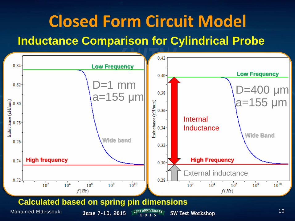
10Mohamed Eldessouki
Inductance Comparison for Cylindrical Probe
D=400 μma=155 μm
Internal Inductance
External inductance
Skin Effect
Wide Band
High Frequency
Low Frequency
Wide band
High frequency
Low Frequency
D=1 mma=155 μm
Calculated based on spring pin dimensions
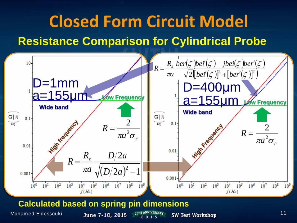
Closed Form Circuit Model
11Mohamed Eldessouki
Resistance Comparison for Cylindrical Probe
D=400μma=155μmWide band
( ) 12
22 −
=aD
aDa
RR s
π
Wide band
D=1mma=155μm
( ) ( ) ( ) ( )( )[ ] ( )[ ]( )222 ζζ
ζζζζπ rbeibe
rbejbeiibebera
RR s
′+′′−′
=
Low Frequency
caR
σπ 22
=ca
Rσπ 2
2=
Low Frequency
Calculated based on spring pin dimensions
Closed Form Circuit Model
12Mohamed Eldessouki
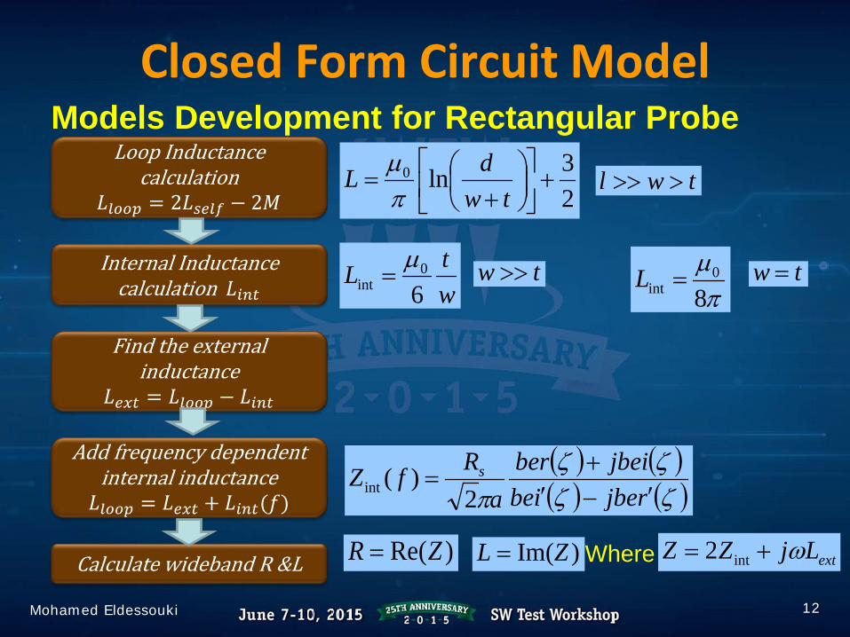
Models Development for Rectangular Probe
23ln0 +
+=
twdL
πµ
wtL
60
intµ
=
( ) ( )( ) ( )ζζ
ζζπ rjbeibe
jbeibera
RfZ s
′−′+
=2
)(int
extLjZZ ω+= int2Where)Re(ZR = )Im(ZL =
πµ8
0int =L
twl >>>
tw >> tw =
Loop Inductance calculation
𝐿𝐿𝑙𝑙𝑙𝑙𝑙𝑙𝑙𝑙 = 2𝐿𝐿𝑠𝑠𝑠𝑠𝑙𝑙𝑠𝑠 − 2𝑀𝑀
Internal Inductance calculation 𝐿𝐿𝑖𝑖𝑖𝑖𝑖𝑖
Find the external inductance
𝐿𝐿𝑠𝑠𝑒𝑒𝑖𝑖 = 𝐿𝐿𝑙𝑙𝑙𝑙𝑙𝑙𝑙𝑙 − 𝐿𝐿𝑖𝑖𝑖𝑖𝑖𝑖
Add frequency dependent internal inductance𝐿𝐿𝑙𝑙𝑙𝑙𝑙𝑙𝑙𝑙 = 𝐿𝐿𝑠𝑠𝑒𝑒𝑖𝑖 + 𝐿𝐿𝑖𝑖𝑖𝑖𝑖𝑖(𝑓𝑓)
Calculate wideband R &L
Closed Form Circuit Model
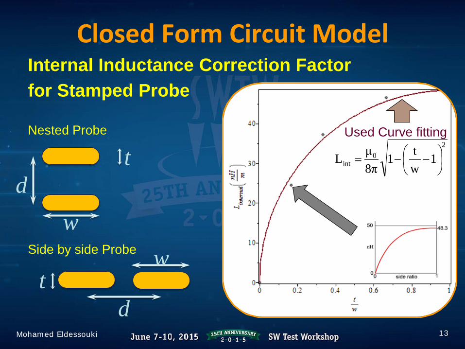
13Mohamed Eldessouki
Internal Inductance Correction Factorfor Stamped Probe
w
td
wt
d
Nested Probe
Side by side Probe
20
int 1wt1
8πμL
−−=
Used Curve fitting
Closed Form Circuit Model
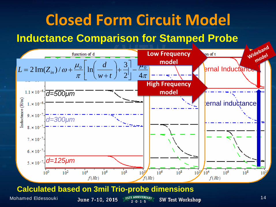
14Mohamed Eldessouki
Inductance Comparison for Stamped Probe
Calculated based on 3mil Trio-probe dimensions
Internal Inductance
External inductance
t=10μm
t=39μm
t=90μm
t=100μm
w=39μm
w=50μm
w=90μmw=100μm
d=125μm
d=300μm
d=500μm
w=1mm
πµ
πµω
423ln/)Im(2 00 −
+
++=
twdZL in
High Frequency model
Low Frequency model
Closed Form Circuit Model
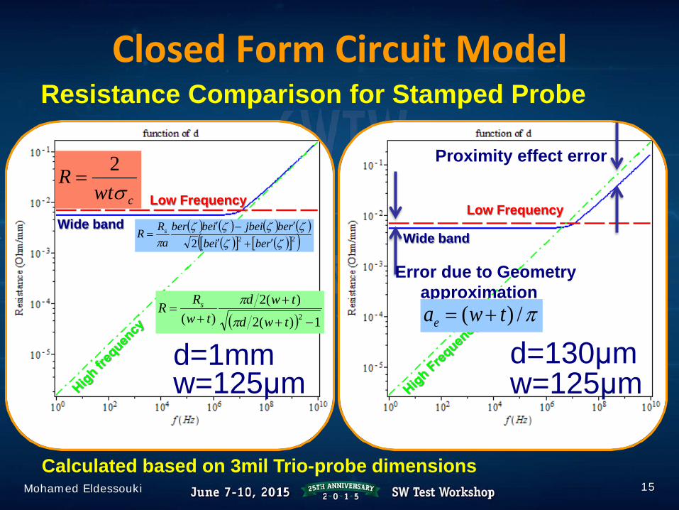
15Mohamed Eldessouki
Resistance Comparison for Stamped Probe
d=130μmw=125μm
Wide bandWide band
d=1mmw=125μm
Low FrequencyLow Frequency
Error due to Geometry approximation
Proximity effect error
( ) ( ) ( ) ( )( )[ ] ( )[ ]( )222 ζζ
ζζζζπ rbeibe
rbejbeiibebera
RR s
′+′′−′
=
cwtR
σ2
=
( ) 1)(2
)(2)( 2 −+
++
=twd
twdtw
RR s
π
ππ/)( twae +=
Calculated based on 3mil Trio-probe dimensions
Closed Form Circuit Model
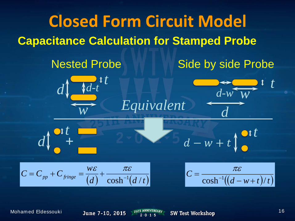
16Mohamed Eldessouki
Capacitance Calculation for Stamped Probe
w
td
Nested Probe Side by side Probe
d-t t
dd-w w
+
( ) ( )tddwCCC fringepp /cosh 1−+=+=
πεε( )( )ttwd
C/cosh 1 +−
= −
πε
dt
𝑑𝑑 − 𝑤𝑤 + 𝑡𝑡t
Equivalent

Closed Form Circuit Model
17Mohamed Eldessouki
Circuit Model Upper Plunger
Barrel
Lower Plunger
Z1
Z2
Z3
Port1
Port2
Probe tail
Stamped section
Probe tip
Measurements & Simulation
18Mohamed Eldessouki
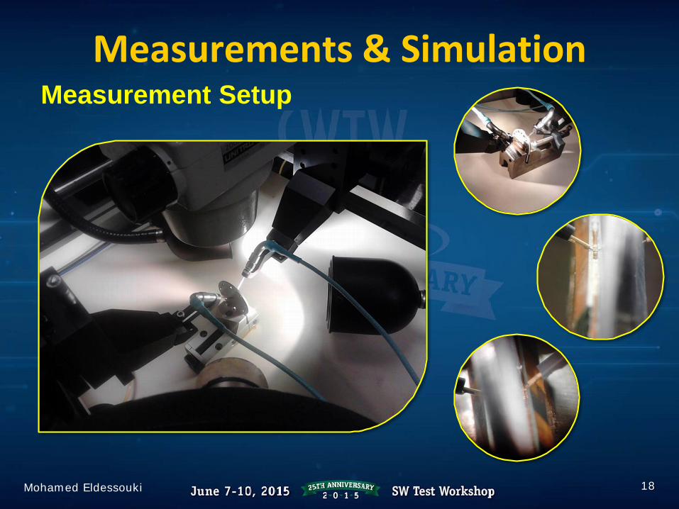
Measurement Setup
Measurements & Simulation
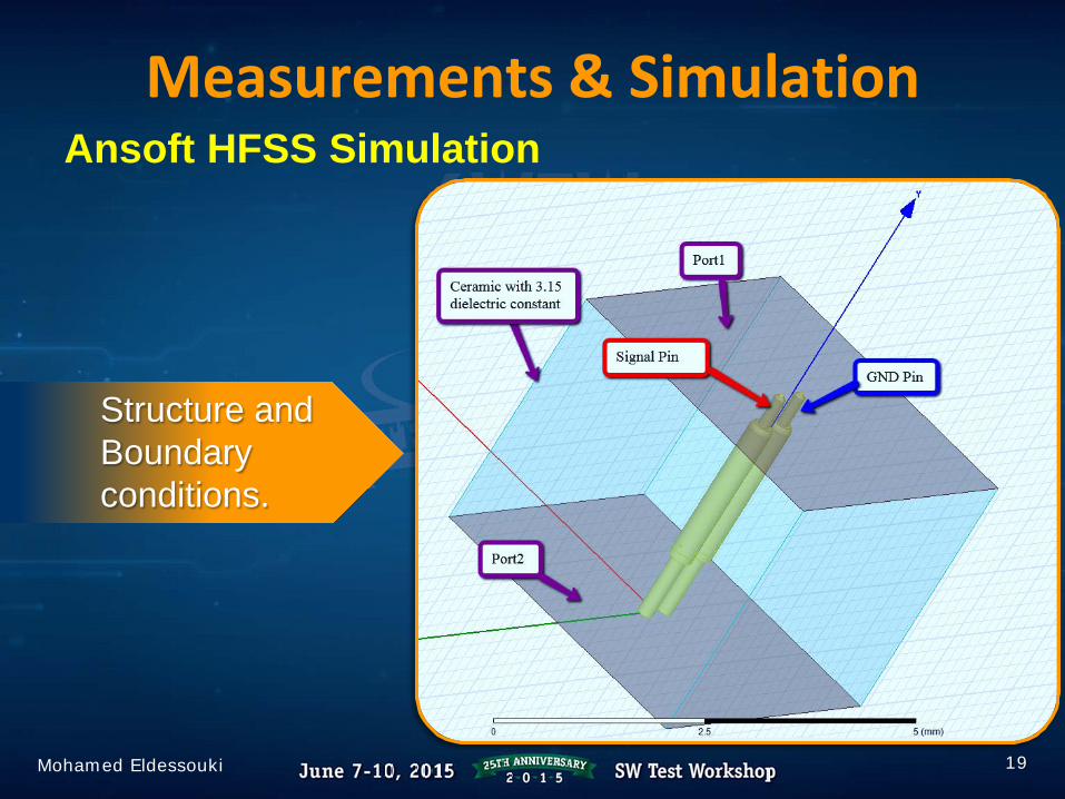
19Mohamed Eldessouki
Ansoft HFSS Simulation
Structure and Boundary conditions.
Measurements & Simulation
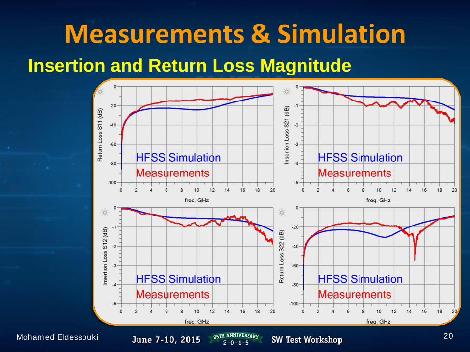
20Mohamed Eldessouki
Insertion and Return Loss Magnitude

Measurements & Simulation
21Mohamed Eldessouki
Insertion and Return Loss Magnitude
Measurements & Simulation
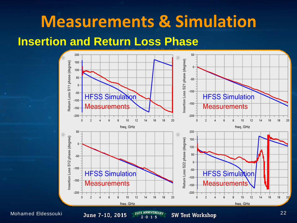
22Mohamed Eldessouki
Insertion and Return Loss Phase
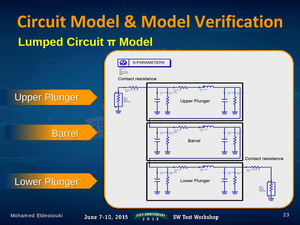
Circuit Model & Model Verification
23Mohamed Eldessouki
Lumped Circuit π Model
Barrel
Lower Plunger
Upper Plunger
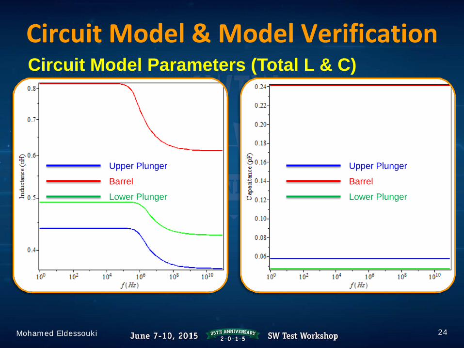
Circuit Model & Model Verification
24Mohamed Eldessouki
Circuit Model Parameters (Total L & C)
Upper Plunger
BarrelLower Plunger
Upper Plunger
BarrelLower Plunger
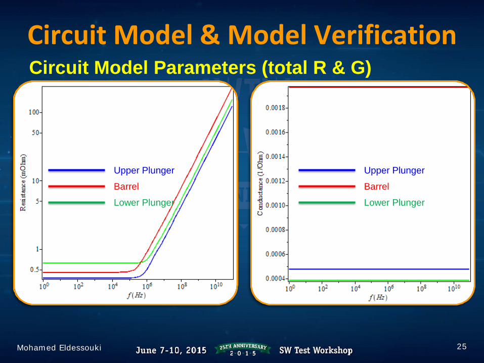
Circuit Model & Model Verification
25Mohamed Eldessouki
Circuit Model Parameters (total R & G)
Upper Plunger
BarrelLower Plunger
Upper Plunger
BarrelLower Plunger
Circuit Model & Model Verification
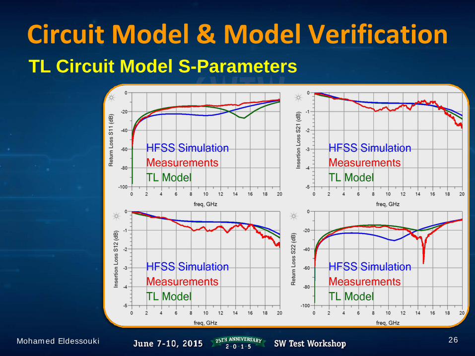
26Mohamed Eldessouki
TL Circuit Model S-Parameters
Circuit Model & Model Verification
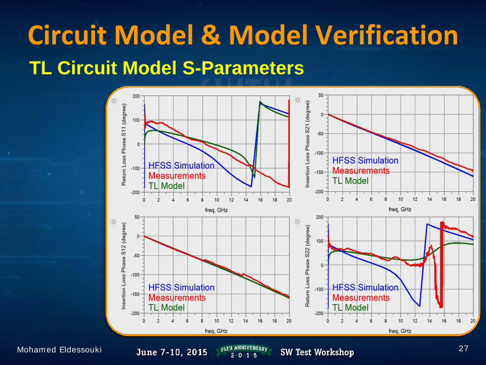
27Mohamed Eldessouki
TL Circuit Model S-Parameters
Circuit Model & Model Verification
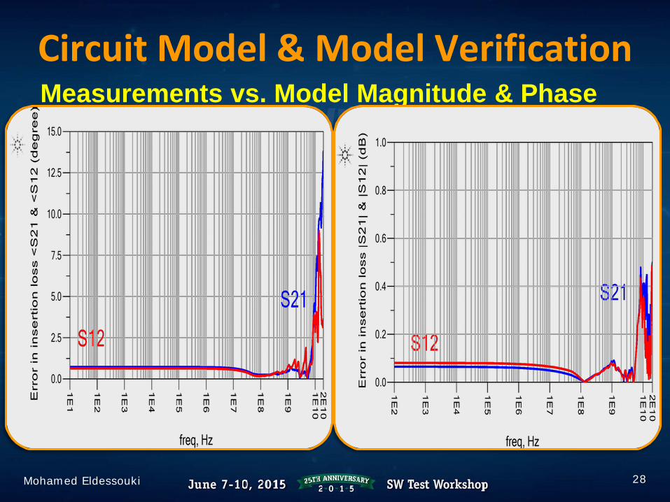
28Mohamed Eldessouki
Measurements vs. Model Magnitude & Phase Error
SUMMARY
29Mohamed Eldessouki
Lumped and TL circuit models had been developed using close form Wideband solution.
Models had been analyzed for 400um probe spacing.
Models were verified against Spring pin measurements and field analysis simulation results.
Results show a good match with maximum magnitude error of 0.5dB and phase error of 12 degree at high frequency
Two models were developed. One for circular cross section and one for rectangular cross section
CONCLUSION
30Mohamed Eldessouki
Using a closed form model, minimize simulation time and cost.
Model can be integrated with other probe card components to obtain a full performance prior to manufacturing to minimize risks and design optimization time delays.
TL model provides better results compared with lumped circuit model, where distribution effect takes place.
Closed form model can be used for quick product feasibility

References
31Mohamed Eldessouki
• Utkarsh R. Patel, Bjrn Gustavsen, and Piero Triverioyz, “An Equivalent Surface Current Approach for the Computation of the Series Impedance of Power Cables with Inclusion of Skin and Proximity Effects”, IEEE Transactions On Power Delivery, 15 August 2013
• M. M. Al-Asadi, A. P. Duffy, A. J. Willis, K. Hodge, and T. M. Benson, “A Simple Formula For Calculating The Frequency-dependent Resistance Of A Round Wire”, Microwave And Optical Technology Letters, Vol. 19, No. 2, October 5 1998
• Pagnetti, A., Xemard, A., Paladian, F., and Nucci, “Evaluation of the impact of proximity effect in the calculation of the internal impedance of cylindrical conductors”, URSI 2011, Aug. 2011.
• C.L. Holloway and E.F. Kuester, "DC Internal Inductance for a Conductor of Rectangular Cross Section", IEEE Transactions on Electromagnetic Compatibility, Vol. 51, No. 2, pp. 338-344, May 2009.
• Z. Piatek, and B. Baron, “Exact closed form formula for self inductance of conductor of rectangular cross section”, Progress In Electromagnetics Research M, Vol. 26, 225-236, 2012
• C. R. Paul, Analysis of Multiconductor Transmission Lines, 2nd ed., Wiley, 2007.
• van der Meijs, N. P.; Fokkema, J. T., “VLSI Circuit Reconstruction From Mask Topology Integration”, VLSI Journal,1984, 2, 85-119.