TPS7A65xx-Q1 300-mA 40-V Low-Dropout Regulator With · PDF file6.2 TSHUTDOWN point 165 ºC...
16
ESR of C ( ) OUT Ω 0.01 0.1 1 10 100 300 0.01 0.1 1 10 V = 14V C = 10 F, 47 F T = 27°C V = 5V, 3.3V IN OUT A OUT μ μ Stable Operation Over Entire Region I (mA) OUT VIN VOUT GND TPS7A65xx CIN COUT VOUT VIN TPS7A6533-Q1 TPS7A6550-Q1 www.ti.com SLVSA98 – MAY 2010 300-mA 40-V LOW-DROPOUT REGULATOR WITH 25-μA QUIESCENT CURRENT Check for Samples: TPS7A6550-Q1 1FEATURES DESCRIPTION • Low Dropout Voltage – 300mV at I OUT = 150mA The TPS7A65xx is a series of low dropout linear voltage regulators designed for low power • 4-V to 40-V Wide Input Voltage Range consumption and quiescent current less than 25 μA in With up to 45-V Transients light load applications. These devices feature an • 300-mA Maximum Output Current integrated over-current protection and are designed • 25-μA (Typ) Ultra Low Quiescent Current at to achieve stable operation even with low-ESR ceramic output capacitors. Low voltage tracking Light Loads feature allows for a smaller input capacitor and can • 3.3-V and 5-V Fixed Output Voltage with ±2% possibly eliminate the need of using a boost Tolerance converter during cold crank conditions. Because of • Low-ESR Ceramic Output Stability Capacitor these features, these devices are well suited in power supplies for various automotive applications. • Integrated Fault Protection – Short-Circuit/Over-Current Protection TYPICAL REGULATOR STABILITY – Thermal Shutdown • Low Input Voltage Tracking • Thermally Enhanced Power Package – 5-pin TO-263 (KTT /D2PAK) – 5-pin TO-252 (KVU /DPAK) APPLICATIONS • Qualified for Automotive Applications • Infotainment Systems with Sleep Mode • Body Control Modules • Always ON Battery Applications – Gateway Applications – Remote Keyless Entry Systems – Immobilizers Figure 1. ESR vs Load Current for TPS7A65xx TYPICAL APPLICATION SCHEMATIC Figure 2. Application Schematic 1 Please be aware that an important notice concerning availability, standard warranty, and use in critical applications of Texas Instruments semiconductor products and disclaimers thereto appears at the end of this data sheet. PRODUCTION DATA information is current as of publication date. Copyright © 2010, Texas Instruments Incorporated Products conform to specifications per the terms of the Texas Instruments standard warranty. Production processing does not necessarily include testing of all parameters. www.BDTIC.com/TI
Transcript of TPS7A65xx-Q1 300-mA 40-V Low-Dropout Regulator With · PDF file6.2 TSHUTDOWN point 165 ºC...
ES
R o
f C
()
OU
TΩ
0.01 0.1 1 10 100 3000.01
0.1
1
10V = 14V
C = 10 F, 47 F
T = 27°C
V = 5V, 3.3V
IN
OUT
A
OUT
µ µ
Stable Operation
Over Entire Region
I (mA)OUT
VIN VOUT
GND
TPS7A65xx
CIN COUT
VOUTVIN
TPS7A6533-Q1TPS7A6550-Q1
www.ti.com SLVSA98 –MAY 2010
300-mA 40-V LOW-DROPOUT REGULATOR WITH 25-µA QUIESCENT CURRENTCheck for Samples: TPS7A6550-Q1
1FEATURESDESCRIPTION• Low Dropout Voltage
– 300mV at IOUT = 150mA The TPS7A65xx is a series of low dropout linearvoltage regulators designed for low power• 4-V to 40-V Wide Input Voltage Rangeconsumption and quiescent current less than 25 µA inWith up to 45-V Transientslight load applications. These devices feature an
• 300-mA Maximum Output Current integrated over-current protection and are designed• 25-µA (Typ) Ultra Low Quiescent Current at to achieve stable operation even with low-ESR
ceramic output capacitors. Low voltage trackingLight Loadsfeature allows for a smaller input capacitor and can• 3.3-V and 5-V Fixed Output Voltage with ±2%possibly eliminate the need of using a boostTolerance converter during cold crank conditions. Because of
• Low-ESR Ceramic Output Stability Capacitor these features, these devices are well suited in powersupplies for various automotive applications.• Integrated Fault Protection
– Short-Circuit/Over-Current ProtectionTYPICAL REGULATOR STABILITY
– Thermal Shutdown• Low Input Voltage Tracking• Thermally Enhanced Power Package
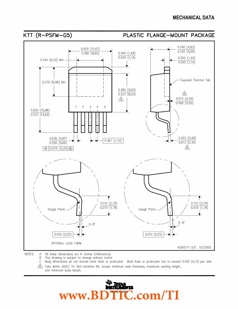
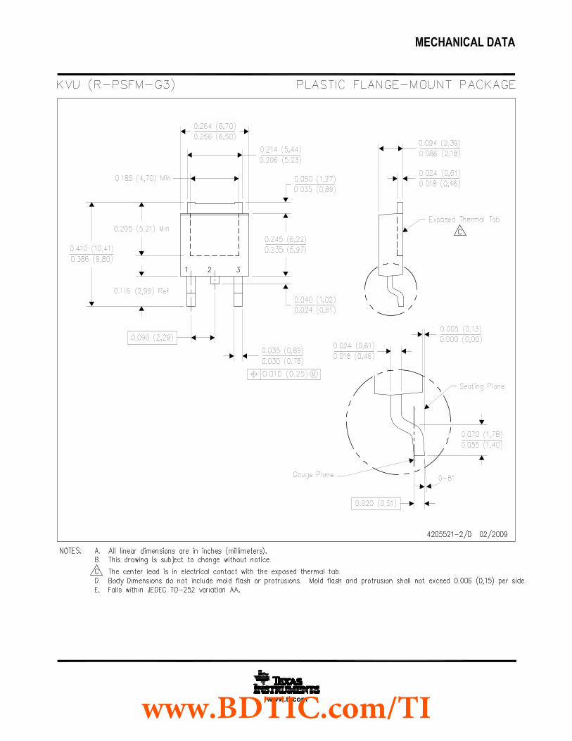
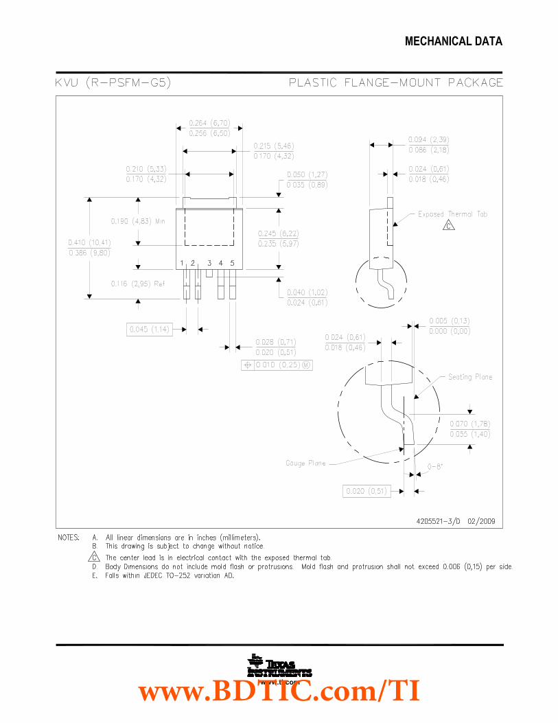
– 5-pin TO-263 (KTT /D2PAK)– 5-pin TO-252 (KVU /DPAK)
APPLICATIONS• Qualified for Automotive Applications• Infotainment Systems with Sleep Mode• Body Control Modules• Always ON Battery Applications
– Gateway Applications– Remote Keyless Entry Systems– Immobilizers
Figure 1. ESR vs Load Current for TPS7A65xx
TYPICAL APPLICATION SCHEMATIC
Figure 2. Application Schematic
1
Please be aware that an important notice concerning availability, standard warranty, and use in critical applications of TexasInstruments semiconductor products and disclaimers thereto appears at the end of this data sheet.
PRODUCTION DATA information is current as of publication date. Copyright © 2010, Texas Instruments IncorporatedProducts conform to specifications per the terms of the TexasInstruments standard warranty. Production processing does notnecessarily include testing of all parameters.www.BDTIC.com/TI
TPS7A6533-Q1TPS7A6550-Q1SLVSA98 –MAY 2010 www.ti.com
ORDERING INFORMATION (1)
OUTPUT VOLTAGE PACKAGE TOP-SIDE MARKING ORDERABLE PART NUMBER (2)
Tube of 70 7A6550Q1 TPS7A6550QKVUQ13 pin KVU
5 V Reel of 2500 Product Preview TPS7A6550QKVURQ1
3 pin KTT Reel of 500 Product Preview TPS7A6550QKTTRQ1
3 pin KTT Reel of 500 Product Preview TPS7A6533QKTTRQ13.3 V
3 pin KVU Reel of 2500 Product Preview TPS7A6533QKVURQ1
(1) For the most current package and ordering information, see the Package Option Addendum at the end of this document, or see the TIweb site at www.ti.com.
(2) Package drawings, thermal data, and symbolization are available at www.ti.com/packaging.
ABSOLUTE MAXIMUM RATINGS (1)
over operating free-air temperature range (unless otherwise noted)
NO. DESCRIPTION VALUE UNIT
1.1 VIN Unregulated input (2) (3) 45 V
1.2 VOUT Regulated output 7 V
Thermal impedance junction to exposed pad KTT (D2PAK) package 10.4 °C/W1.3 qJP
Thermal impedance junction to exposed pad KVU (DPAK) package 12.7 °C/W
Thermal impedance junction to ambient KTT (D2PAK) package (4) 30.2 °C/W1.4 qJA
Thermal impedance junction to ambient KVU (DPAK) package (4) 29.3 °C/W
Thermal impedance junction to ambient KTT (D2PAK) package (5) 34.4 °C/W1.5 qJA
Thermal impedance junction to ambient KVU (DPAK) package (5) 38.6 °C/W
1.6 ESD Electrostatic discharge (6) 2 kV
1.7 TOP Operating ambient temperature 125 °C
1.8 TS Storage temperature range -65 to +150 °C
(1) Stresses beyond those listed under absolute maximum ratings may cause permanent damage to the device. These are stress ratingsonly, and functional operation of the device at these or any other conditions beyond those indicated under recommended operatingconditions is not implied. Exposure to absolute-maximum-rated conditions for extended periods may affect device reliability. All voltagevalues are with respect to GND.
(2) Absolute negative voltage on these pins not to go below –0.3V.(3) Absolute maximum voltage for duration less than 480ms.(4) The thermal data is based on JEDEC standard high K profile – JESD 51-5. The copper pad is soldered to the thermal land pattern. Also
correct attachment procedure needs to be incorporated.(5) The thermal data is based on JEDEC standard low K profile – JESD 51-3. The copper pad is soldered to the thermal land pattern. Also
correct attachment procedure needs to be incorporated.(6) The human body model is a 100pF capacitor discharged through a 1.5kΩ resistor into each pin.
DISSIPATION RATINGSDERATING FACTORTA < 25°C POWER TA = 85°C POWERNO. JEDEC STANDARD PACKAGE ABOVE TA = 25°CRATING (W) RATING (W)(°C/W)
2.1 3 pin KTT 3.63 34.4 1.89JEDEC Standard PCB -low K, JESD 51-32.2 3 pin KVU 3.24 38.6 1.68
2.3 3 pin KTT 4.14 30.2 2.15JEDEC Standard PCB -high K, JESD 51-52.4 3 pin KVU 4.27 29.3 2.22
RECOMMENDED OPERATING CONDITIONSNO. DESCRIPTION MIN MAX UNIT
3.1 VIN Unregulated input voltage 4 40 V
3.2 TJ Operating junction temperature range -40 150 °C
2 Submit Documentation Feedback Copyright © 2010, Texas Instruments Incorporated
Product Folder Link(s) :TPS7A6550-Q1www.BDTIC.com/TI
TPS7A6533-Q1TPS7A6550-Q1
www.ti.com SLVSA98 –MAY 2010
ELECTRICAL CHARACTERISTICSVIN = 14V, TJ = -40ºC to 150ºC (unless otherwise noted)
NO. PARAMETER TEST CONDITIONS MIN TYP MAX UNIT
4. Input Voltage (VIN pin)
Fixed 5V output, IOUT = 1mA 5.3 404.1 VIN Input voltage V
Fixed 3.3V output, IOUT = 1mA (Preview Only) 3.6 40
4.2 IQUIESCENT Quiescent current VIN = 8.2V to 18V, IOUT = 0.01mA to 0.75mA 25 40 µA
Under voltage lock out4.3 VIN-UVLO Ramp VIN down until output is turned OFF 3.16 Vvoltage
4.4 VIN(POWERUP) Power up voltage Ramp VIN up until output is turned ON 3.45 V
5. Regulated Output Voltage (VOUT pin)
Fixed VOUT value (3.3V or 5V as applicable),5.1 VOUT Regulated output voltage -2 2 %IOUT = 10mA
VIN = 6V to 28V, IOUT = 10mA, VOUT = 5V 15 mV5.2 ∆VLINE-REG Line regulation VIN = 6V to 28V, IOUT = 10mA, VOUT = 3.3V 20 mV(Preview Only)
IOUT = 10mA to 300mA, VIN= 14V, VOUT = 5V 25 mV5.3 ∆VLOAD-REG Load regulation IOUT = 10mA to 300mA,VIN = 14V, VOUT = 3.3V 35 mV(Preview Only)
IOUT = 250mA 500 mVDropout voltage5.4 VDROPOUT(1)
(VIN – VOUT) IOUT = 150mA 300 mV
5.5 RSW(2) Switch resistance VIN to VOUT resistance 2 Ω
5.6 IOUT Output current VOUT in regulation 0 300 mA
5.7 ICL Output current limit VOUT = 0V (VOUT pin is shorted to ground) 350 1000 mA
VIN-RIPPLE = 0.5 Vpp, IOUT = 300mA,frequency = 100 Hz, VOUT = 5V and 60VOUT = 3.3V (Preview Only)Power supply ripple5.8 PSRR (2) dBrejection VIN-RIPPLE = 0.5 Vpp, IOUT = 300mA,frequency = 150 kHz, VOUT = 5V and 30VOUT = 3.3V (Preview Only)
6. Operating Temperature Range
Operating junction6.1 TJ -40 150 ºCtemperature
Thermal shutdown trip6.2 TSHUTDOWN 165 ºCpoint
Thermal shutdown6.3 THYST 10 ºChysteresis
(1) This test is done with VOUT in regulation and VIN – VOUT parameter is measured when VOUT (3.3 V or 5.0 V) drops by 100 mV atspecified loads.
(2) Specified by design – not tested
Copyright © 2010, Texas Instruments Incorporated Submit Documentation Feedback 3
Product Folder Link(s) :TPS7A6550-Q1www.BDTIC.com/TI
GND
VOUTVIN
1 2 3
GND VOUTVIN
1 2 3
Q1
Oscillator
UVLOComp. with
InternalReference
LogicControl
Band Gap
Over Current Detection
VRef1
RegulatorControl
VIN
VOUT
CIN
COUT
VIN
VOUT
GND
VRef1
ChargePump
ErrorAmp
Temperature Sensor/Thermal Shutdown
TPS7A6533-Q1TPS7A6550-Q1SLVSA98 –MAY 2010 www.ti.com
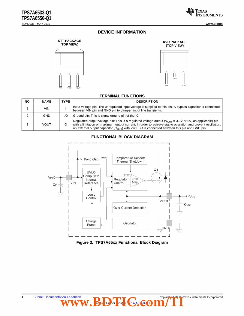
DEVICE INFORMATION
KTT PACKAGE KVU PACKAGE(TOP VIEW) (TOP VIEW)
TERMINAL FUNCTIONSNO. NAME TYPE DESCRIPTION
Input voltage pin: The unregulated input voltage is supplied to this pin. A bypass capacitor is connected1 VIN I between VIN pin and GND pin to dampen input line transients.
2 GND I/O Ground pin: This is signal ground pin of the IC.
Regulated output voltage pin: This is a regulated voltage output (VOUT = 3.3V or 5V, as applicable) pin3 VOUT O with a limitation on maximum output current. In order to achieve stable operation and prevent oscillation,
an external output capacitor (COUT) with low ESR is connected between this pin and GND pin.
FUNCTIONAL BLOCK DIAGRAM
Figure 3. TPS7A65xx Functional Block Diagram
4 Submit Documentation Feedback Copyright © 2010, Texas Instruments Incorporated
Product Folder Link(s) :TPS7A6550-Q1www.BDTIC.com/TI
I (mA)OUT
ES
R o
f C
(Ω)
OU
T
0.01 0.1 1 10 100 3000.01
0.1
1
10
30
0.03
0.06
V = 14V
C = 1µF
T = 27°C
V = 5V
IN
OUT
A
OUT
Stable Operation
UnstableOperation
I (mA)OUT
ES
R o
f C
(Ω)
OU
T
0.01 0.1 1 10 100 3000.01
0.1
1
10
30
0.03
0.06
V = 14V
C = 1µF
T = 27°C
V = 3.3V
IN
OUT
A
OUT
Stable Operation
Unstable
Operation
15
20
25
30
35
40
45
50
55
-50 0 50 100 150
TA (°C)
VIN =14V
VOUT=5V, 3.3V
IOUT = 1mA
IOUT = 250mA
I(µ
A)
QU
IES
CE
NT
0
10
20
30
40
50
60
70
80
0.001 0.01 0.1 1 10 100 1000
IOUT (mA)
VIN = 14VTA= 25°CVOUT = 5V, 3.3V
I(µ
A)
QU
IES
CE
NT
0
100
200
300
400
500
600
700
4 14 24 34V IN (V)
VOUT = 5V, 3.3V
TA= 25°C
IOUT = 100mA
No Load
I(µ
A)
QU
IES
CE
NT
40
0
0.05
0.1
0.15
0.2
0.25
0.3
0.35
0.4
0 50 100 150 200 250 300
IOUT (mA)
VD
RO
PO
UT
(V)
TA = 25°C
VOUT = 5V
TA = 125°C
TA = -40°C
TPS7A6533-Q1TPS7A6550-Q1
www.ti.com SLVSA98 –MAY 2010
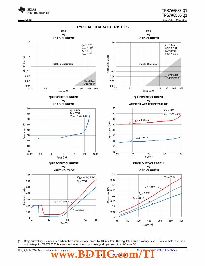
TYPICAL CHARACTERISTICSESR ESRvs vs
LOAD CURRENT LOAD CURRENT
QUIESCENT CURRENT QUIESCENT CURRENTvs vs
LOAD CURRENT AMBIENT AIR TEMPERATURE
QUIESCENT CURRENT DROP OUT VOLTAGE (1)
vs vsINPUT VOLTAGE LOAD CURRENT
(1) Drop out voltage is measured when the output voltage drops by 100mV from the regulated output voltage level. (For example, the dropout voltage for TPS7A6550 is measured when the output voltage drops down to 4.9V from 5V.)
Copyright © 2010, Texas Instruments Incorporated Submit Documentation Feedback 5
Product Folder Link(s) :TPS7A6550-Q1www.BDTIC.com/TI
4.9
4.92
4.94
4.96
4.98
5
5.02
5.04
5.06
5.08
5.1
-50 0 50 100 150
TA (°C)
VO
UT
(V)
VIN = 14V
IOUT = 1mA
0
5
6
2 3 4 5 6 7
V IN (V)
1
2
3
4
VO
UT
(V)
IOUT = 100mA
TA = 25°C
0
0.02
0.04
0.06
0.08
0.1
0.12
0 10 20 30 40 50
V (V)IN
ILOAD = 100mA
VOUT = 5V, 3.3V
TA= 25°C
TA = -40°C
TA= 125°C
I(A
)O
UT
450
500
550
600
650
700
750
-50 0 50 100 150
TA (°C)
I CL
(mA
)
V = 14V
V = 5V, 3.3VIN
OUT
8
8.5
9
9.5
10
10.5
11
11.5
12
-50 0 50 100 150
TA (°C)
Lo
ad
Re
gu
lati
on
(mV
)
VIN = 14VVOUT = 5V, 3.3VIOUT step from10mA to 300mA
0
0.5
1
1.5
2
2.5
3
-50 0 50 100 150
TA (°C)
IOUT = 10mAVOUT = 5V, 3.3VVIN step from8V to 28V
Lin
e R
eg
ula
tio
n (
mV
)
TPS7A6533-Q1TPS7A6550-Q1SLVSA98 –MAY 2010 www.ti.com
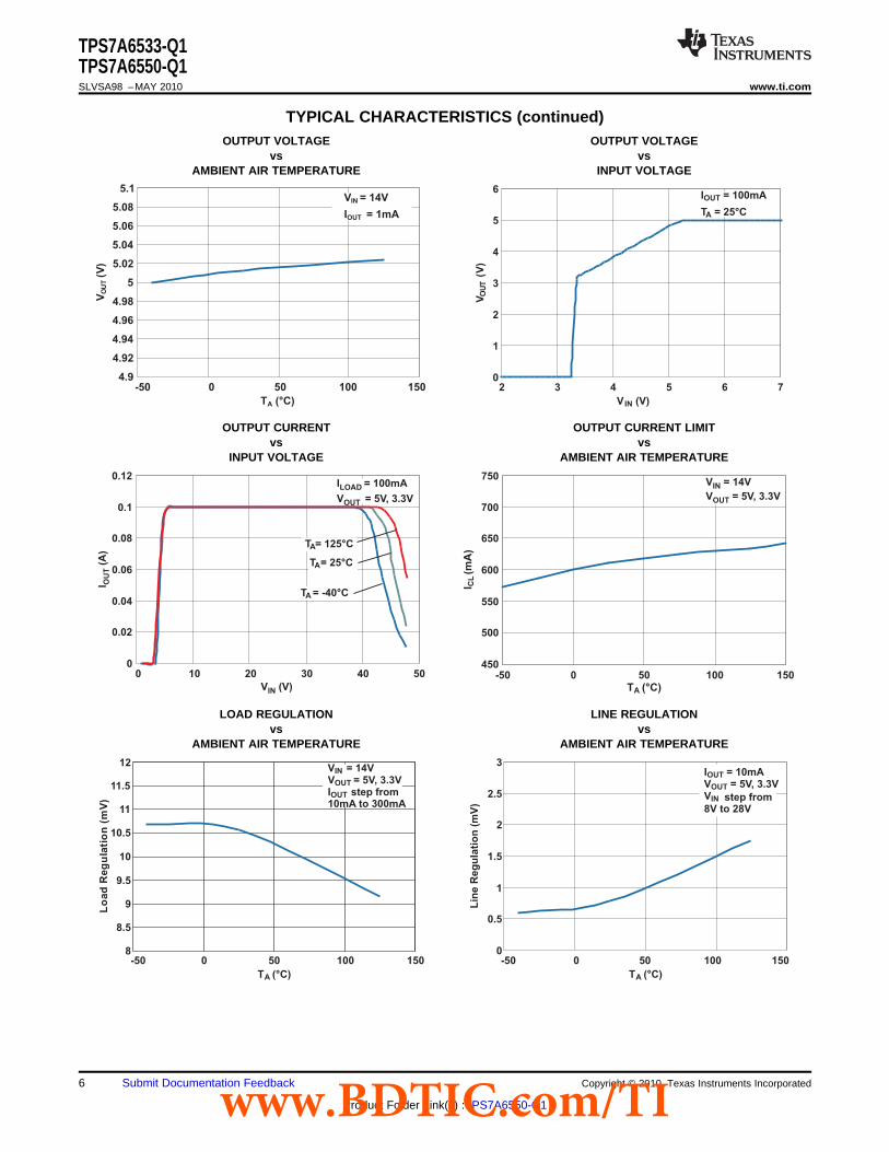
TYPICAL CHARACTERISTICS (continued)OUTPUT VOLTAGE OUTPUT VOLTAGE
vs vsAMBIENT AIR TEMPERATURE INPUT VOLTAGE
OUTPUT CURRENT OUTPUT CURRENT LIMITvs vs
INPUT VOLTAGE AMBIENT AIR TEMPERATURE
LOAD REGULATION LINE REGULATIONvs vs
AMBIENT AIR TEMPERATURE AMBIENT AIR TEMPERATURE
6 Submit Documentation Feedback Copyright © 2010, Texas Instruments Incorporated
Product Folder Link(s) :TPS7A6550-Q1www.BDTIC.com/TI
0
20
40
60
80
100
120
10 100 1k 10k 100k 1M
Frequency (Hz)
PS
RR
(dB
)
VIN = 14VIOUT = 250mATA = 25°CCOUT = 10µFVOUT = 5V, 3.3V
0
20
40
60
80
100
120
Frequency (Hz)
PS
RR
(dB
)
VIN = 14VIOUT = 1mATA = 25°CCOUT = 10µFVOUT = 5V, 3.3V
10 100 1k 10k 100k 1M
TPS7A6533-Q1TPS7A6550-Q1
www.ti.com SLVSA98 –MAY 2010
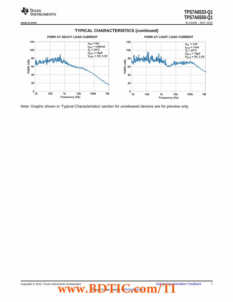
TYPICAL CHARACTERISTICS (continued)PSRR AT HEAVY LOAD CURRENT PSRR AT LIGHT LOAD CURRENT
Note: Graphs shown in 'Typical Characteristics' section for unreleased devices are for preview only.
Copyright © 2010, Texas Instruments Incorporated Submit Documentation Feedback 7
Product Folder Link(s) :TPS7A6550-Q1www.BDTIC.com/TI
ON
OFFCh
arg
e P
um
p S
tate
7.8 7.9
Hysteresis
V (V)IN
ON
OFFCh
arg
e P
um
p S
tate
9.2 9.6
Hysteresis
V (V)IN
VIN(POWERUP)
VIN
VOUT
5V or 3.3V
0
0
TPS7A6533-Q1TPS7A6550-Q1SLVSA98 –MAY 2010 www.ti.com
DETAILED DESCRIPTION
TPS7A65xx is a series of monolithic low dropoutlinear voltage regulators designed for low powerconsumption and quiescent current less than 25µA inlight load applications. Because of an integrated faultprotection, these devices are well suited in powersupplies for various automotive applications.
These devices are available in two fixed outputvoltage versions as follows:• 5V Output version (TPS7A6550)• 3.3V Output version (TPS7A6533)
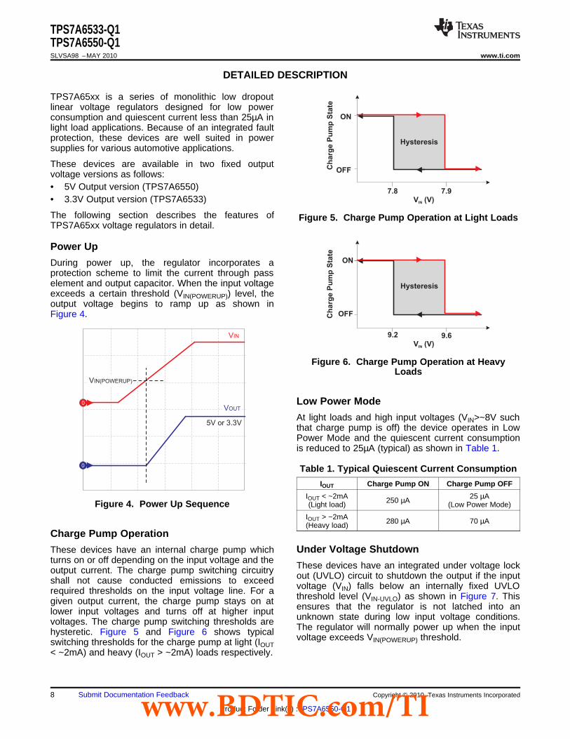
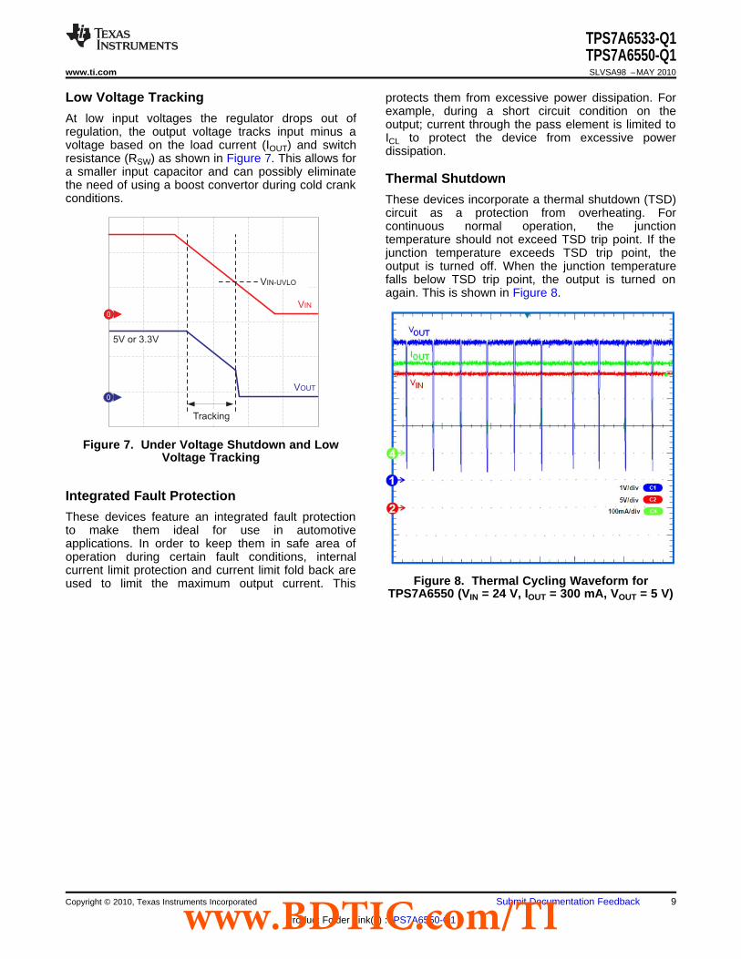
The following section describes the features of Figure 5. Charge Pump Operation at Light LoadsTPS7A65xx voltage regulators in detail.
Power Up
During power up, the regulator incorporates aprotection scheme to limit the current through passelement and output capacitor. When the input voltageexceeds a certain threshold (VIN(POWERUP)) level, theoutput voltage begins to ramp up as shown inFigure 4.
Figure 6. Charge Pump Operation at HeavyLoads
Low Power Mode
At light loads and high input voltages (VIN>~8V suchthat charge pump is off) the device operates in LowPower Mode and the quiescent current consumptionis reduced to 25µA (typical) as shown in Table 1.
Table 1. Typical Quiescent Current Consumption
IOUT Charge Pump ON Charge Pump OFF
IOUT < ~2mA 25 µA250 µAFigure 4. Power Up Sequence (Light load) (Low Power Mode)
IOUT > ~2mA 280 µA 70 µA(Heavy load)Charge Pump Operation
Under Voltage ShutdownThese devices have an internal charge pump whichturns on or off depending on the input voltage and the
These devices have an integrated under voltage lockoutput current. The charge pump switching circuitryout (UVLO) circuit to shutdown the output if the inputshall not cause conducted emissions to exceedvoltage (VIN) falls below an internally fixed UVLOrequired thresholds on the input voltage line. For athreshold level (VIN-UVLO) as shown in Figure 7. Thisgiven output current, the charge pump stays on atensures that the regulator is not latched into anlower input voltages and turns off at higher inputunknown state during low input voltage conditions.voltages. The charge pump switching thresholds areThe regulator will normally power up when the inputhysteretic. Figure 5 and Figure 6 shows typicalvoltage exceeds VIN(POWERUP) threshold.switching thresholds for the charge pump at light (IOUT
< ~2mA) and heavy (IOUT > ~2mA) loads respectively.
8 Submit Documentation Feedback Copyright © 2010, Texas Instruments Incorporated
Product Folder Link(s) :TPS7A6550-Q1www.BDTIC.com/TI
VIN
VOUT
VIN-UVLO
5V or 3.3V
Tracking
0
0
TPS7A6533-Q1TPS7A6550-Q1
www.ti.com SLVSA98 –MAY 2010
Low Voltage Tracking protects them from excessive power dissipation. Forexample, during a short circuit condition on the
At low input voltages the regulator drops out of output; current through the pass element is limited toregulation, the output voltage tracks input minus a ICL to protect the device from excessive powervoltage based on the load current (IOUT) and switch dissipation.resistance (RSW) as shown in Figure 7. This allows fora smaller input capacitor and can possibly eliminate Thermal Shutdownthe need of using a boost convertor during cold crankconditions. These devices incorporate a thermal shutdown (TSD)
circuit as a protection from overheating. Forcontinuous normal operation, the junctiontemperature should not exceed TSD trip point. If thejunction temperature exceeds TSD trip point, theoutput is turned off. When the junction temperaturefalls below TSD trip point, the output is turned onagain. This is shown in Figure 8.
Figure 7. Under Voltage Shutdown and LowVoltage Tracking
Integrated Fault Protection
These devices feature an integrated fault protectionto make them ideal for use in automotiveapplications. In order to keep them in safe area ofoperation during certain fault conditions, internalcurrent limit protection and current limit fold back are
Figure 8. Thermal Cycling Waveform forused to limit the maximum output current. ThisTPS7A6550 (VIN = 24 V, IOUT = 300 mA, VOUT = 5 V)
Copyright © 2010, Texas Instruments Incorporated Submit Documentation Feedback 9
Product Folder Link(s) :TPS7A6550-Q1www.BDTIC.com/TI
1µFto
10µF
0.1µF 0.1µF
VIN VOUT
GND
TPS7A65xx
VOUTVIN
10µFto
22µF
0
0.5
1
1.5
2
2.5
3
3.5
4
0 25 50 75 100 125
Ambient Air Temperature (°C)
JESD 51-5 (KTT)
JESD 51-3 (KVU)
JESD 51-5 (KVU)
JESD 51-3 (KTT)
Po
wer
Dis
sip
ate
d (
W)
150
TPS7A6533-Q1TPS7A6550-Q1SLVSA98 –MAY 2010 www.ti.com
APPLICATION INFORMATION
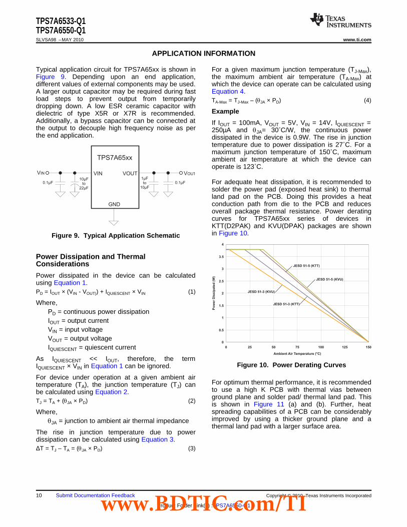
Typical application circuit for TPS7A65xx is shown in For a given maximum junction temperature (TJ-Max),Figure 9. Depending upon an end application, the maximum ambient air temperature (TA-Max) atdifferent values of external components may be used. which the device can operate can be calculated usingA larger output capacitor may be required during fast Equation 4.load steps to prevent output from temporarily TA-Max = TJ-Max – (qJA × PD) (4)dropping down. A low ESR ceramic capacitor with
Exampledielectric of type X5R or X7R is recommended.Additionally, a bypass capacitor can be connected at If IOUT = 100mA, VOUT = 5V, VIN = 14V, IQUIESCENT =the output to decouple high frequency noise as per 250µA and qJA= 30˚C/W, the continuous powerthe end application. dissipated in the device is 0.9W. The rise in junction
temperature due to power dissipation is 27˚C. For amaximum junction temperature of 150˚C, maximumambient air temperature at which the device canoperate is 123˚C.
For adequate heat dissipation, it is recommended tosolder the power pad (exposed heat sink) to thermalland pad on the PCB. Doing this provides a heatconduction path from die to the PCB and reducesoverall package thermal resistance. Power deratingcurves for TPS7A65xx series of devices inKTT(D2PAK) and KVU(DPAK) packages are shownin Figure 10.Figure 9. Typical Application Schematic
Power Dissipation and ThermalConsiderations
Power dissipated in the device can be calculatedusing Equation 1.PD = IOUT × (VIN - VOUT)) + IQUIESCENT × VIN (1)
Where,PD = continuous power dissipationIOUT = output currentVIN = input voltageVOUT = output voltageIQUIESCENT = quiescent current
As IQUIESCENT << IOUT, therefore, the termFigure 10. Power Derating CurvesIQUIESCENT × VIN in Equation 1 can be ignored.
For device under operation at a given ambient airFor optimum thermal performance, it is recommendedtemperature (TA), the junction temperature (TJ) canto use a high K PCB with thermal vias betweenbe calculated using Equation 2.ground plane and solder pad/ thermal land pad. This
TJ = TA + (qJA × PD) (2) is shown in Figure 11 (a) and (b). Further, heatspreading capabilities of a PCB can be considerablyWhere,improved by using a thicker ground plane and aqJA = junction to ambient air thermal impedancethermal land pad with a larger surface area.
The rise in junction temperature due to powerdissipation can be calculated using Equation 3.ΔT = TJ – TA = (qJA × PD) (3)
10 Submit Documentation Feedback Copyright © 2010, Texas Instruments Incorporated
Product Folder Link(s) :TPS7A6550-Q1www.BDTIC.com/TI
PCB
Thermal Land Pad
Exposed Tab
Thermal Via
(a) Before soldering
(b) After soldering
Ground Plane
30
35
40
45
50
55
0 200 400 600 800 1000
Thermal Pad Area (sq. mm)
qJ
A(°
C/W
)
KTT (D2PAK) (JESD 51-3)
KVU (DPAK) (JESD 51-3)
TPS7A6533-Q1TPS7A6550-Q1
www.ti.com SLVSA98 –MAY 2010
Keeping other factors constant, surface area of thethermal land pad contributes to heat dissipation onlyto a certain extent. Figure 12 shows variation of qJAwith surface area of the thermal land pad (soldered tothe exposed pad) for KTT and KVU packages.
Figure 11. Using Multilayer PCB and ThermalVias For Adequate Heat Dissipation
Figure 12. qJA vs Thermal Pad Area
Copyright © 2010, Texas Instruments Incorporated Submit Documentation Feedback 11
Product Folder Link(s) :TPS7A6550-Q1www.BDTIC.com/TI
PACKAGE OPTION ADDENDUM
www.ti.com 12-Jul-2010
Addendum-Page 1
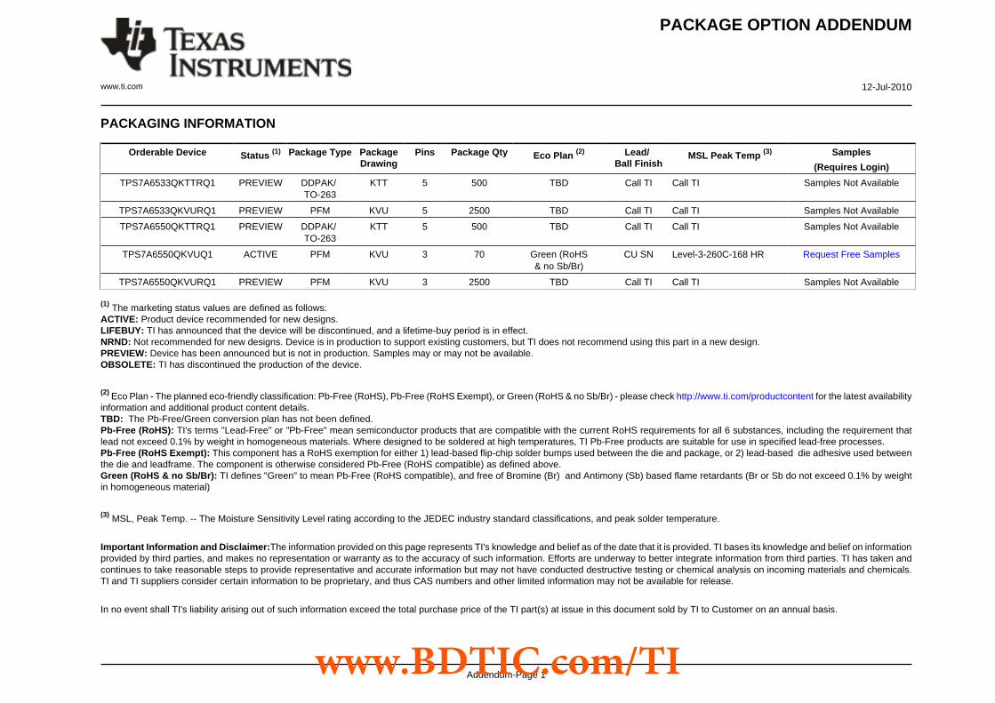
PACKAGING INFORMATION
Orderable Device Status (1) Package Type PackageDrawing
Pins Package Qty Eco Plan (2) Lead/Ball Finish
MSL Peak Temp (3) Samples
(Requires Login)
TPS7A6533QKTTRQ1 PREVIEW DDPAK/TO-263
KTT 5 500 TBD Call TI Call TI Samples Not Available
TPS7A6533QKVURQ1 PREVIEW PFM KVU 5 2500 TBD Call TI Call TI Samples Not Available
TPS7A6550QKTTRQ1 PREVIEW DDPAK/TO-263
KTT 5 500 TBD Call TI Call TI Samples Not Available
TPS7A6550QKVUQ1 ACTIVE PFM KVU 3 70 Green (RoHS& no Sb/Br)
CU SN Level-3-260C-168 HR Request Free Samples
TPS7A6550QKVURQ1 PREVIEW PFM KVU 3 2500 TBD Call TI Call TI Samples Not Available (1) The marketing status values are defined as follows:ACTIVE: Product device recommended for new designs.LIFEBUY: TI has announced that the device will be discontinued, and a lifetime-buy period is in effect.NRND: Not recommended for new designs. Device is in production to support existing customers, but TI does not recommend using this part in a new design.PREVIEW: Device has been announced but is not in production. Samples may or may not be available.OBSOLETE: TI has discontinued the production of the device.
(2) Eco Plan - The planned eco-friendly classification: Pb-Free (RoHS), Pb-Free (RoHS Exempt), or Green (RoHS & no Sb/Br) - please check http://www.ti.com/productcontent for the latest availabilityinformation and additional product content details.TBD: The Pb-Free/Green conversion plan has not been defined.Pb-Free (RoHS): TI's terms "Lead-Free" or "Pb-Free" mean semiconductor products that are compatible with the current RoHS requirements for all 6 substances, including the requirement thatlead not exceed 0.1% by weight in homogeneous materials. Where designed to be soldered at high temperatures, TI Pb-Free products are suitable for use in specified lead-free processes.Pb-Free (RoHS Exempt): This component has a RoHS exemption for either 1) lead-based flip-chip solder bumps used between the die and package, or 2) lead-based die adhesive used betweenthe die and leadframe. The component is otherwise considered Pb-Free (RoHS compatible) as defined above.Green (RoHS & no Sb/Br): TI defines "Green" to mean Pb-Free (RoHS compatible), and free of Bromine (Br) and Antimony (Sb) based flame retardants (Br or Sb do not exceed 0.1% by weightin homogeneous material)
(3) MSL, Peak Temp. -- The Moisture Sensitivity Level rating according to the JEDEC industry standard classifications, and peak solder temperature.
Important Information and Disclaimer:The information provided on this page represents TI's knowledge and belief as of the date that it is provided. TI bases its knowledge and belief on informationprovided by third parties, and makes no representation or warranty as to the accuracy of such information. Efforts are underway to better integrate information from third parties. TI has taken andcontinues to take reasonable steps to provide representative and accurate information but may not have conducted destructive testing or chemical analysis on incoming materials and chemicals.TI and TI suppliers consider certain information to be proprietary, and thus CAS numbers and other limited information may not be available for release.
In no event shall TI's liability arising out of such information exceed the total purchase price of the TI part(s) at issue in this document sold by TI to Customer on an annual basis.
www.BDTIC.com/TI
www.BDTIC.com/TI
www.BDTIC.com/TI
www.BDTIC.com/TI
IMPORTANT NOTICE
Texas Instruments Incorporated and its subsidiaries (TI) reserve the right to make corrections, modifications, enhancements, improvements,and other changes to its products and services at any time and to discontinue any product or service without notice. Customers shouldobtain the latest relevant information before placing orders and should verify that such information is current and complete. All products aresold subject to TI’s terms and conditions of sale supplied at the time of order acknowledgment.
TI warrants performance of its hardware products to the specifications applicable at the time of sale in accordance with TI’s standardwarranty. Testing and other quality control techniques are used to the extent TI deems necessary to support this warranty. Except wheremandated by government requirements, testing of all parameters of each product is not necessarily performed.
TI assumes no liability for applications assistance or customer product design. Customers are responsible for their products andapplications using TI components. To minimize the risks associated with customer products and applications, customers should provideadequate design and operating safeguards.
TI does not warrant or represent that any license, either express or implied, is granted under any TI patent right, copyright, mask work right,or other TI intellectual property right relating to any combination, machine, or process in which TI products or services are used. Informationpublished by TI regarding third-party products or services does not constitute a license from TI to use such products or services or awarranty or endorsement thereof. Use of such information may require a license from a third party under the patents or other intellectualproperty of the third party, or a license from TI under the patents or other intellectual property of TI.
Reproduction of TI information in TI data books or data sheets is permissible only if reproduction is without alteration and is accompaniedby all associated warranties, conditions, limitations, and notices. Reproduction of this information with alteration is an unfair and deceptivebusiness practice. TI is not responsible or liable for such altered documentation. Information of third parties may be subject to additionalrestrictions.
Resale of TI products or services with statements different from or beyond the parameters stated by TI for that product or service voids allexpress and any implied warranties for the associated TI product or service and is an unfair and deceptive business practice. TI is notresponsible or liable for any such statements.
TI products are not authorized for use in safety-critical applications (such as life support) where a failure of the TI product would reasonablybe expected to cause severe personal injury or death, unless officers of the parties have executed an agreement specifically governingsuch use. Buyers represent that they have all necessary expertise in the safety and regulatory ramifications of their applications, andacknowledge and agree that they are solely responsible for all legal, regulatory and safety-related requirements concerning their productsand any use of TI products in such safety-critical applications, notwithstanding any applications-related information or support that may beprovided by TI. Further, Buyers must fully indemnify TI and its representatives against any damages arising out of the use of TI products insuch safety-critical applications.
TI products are neither designed nor intended for use in military/aerospace applications or environments unless the TI products arespecifically designated by TI as military-grade or "enhanced plastic." Only products designated by TI as military-grade meet militaryspecifications. Buyers acknowledge and agree that any such use of TI products which TI has not designated as military-grade is solely atthe Buyer's risk, and that they are solely responsible for compliance with all legal and regulatory requirements in connection with such use.
TI products are neither designed nor intended for use in automotive applications or environments unless the specific TI products aredesignated by TI as compliant with ISO/TS 16949 requirements. Buyers acknowledge and agree that, if they use any non-designatedproducts in automotive applications, TI will not be responsible for any failure to meet such requirements.
Following are URLs where you can obtain information on other Texas Instruments products and application solutions:
Products Applications
Amplifiers amplifier.ti.com Audio www.ti.com/audio
Data Converters dataconverter.ti.com Automotive www.ti.com/automotive
DLP® Products www.dlp.com Communications and www.ti.com/communicationsTelecom
DSP dsp.ti.com Computers and www.ti.com/computersPeripherals
Clocks and Timers www.ti.com/clocks Consumer Electronics www.ti.com/consumer-apps
Interface interface.ti.com Energy www.ti.com/energy
Logic logic.ti.com Industrial www.ti.com/industrial
Power Mgmt power.ti.com Medical www.ti.com/medical
Microcontrollers microcontroller.ti.com Security www.ti.com/security
RFID www.ti-rfid.com Space, Avionics & www.ti.com/space-avionics-defenseDefense
RF/IF and ZigBee® Solutions www.ti.com/lprf Video and Imaging www.ti.com/video
Wireless www.ti.com/wireless-apps
Mailing Address: Texas Instruments, Post Office Box 655303, Dallas, Texas 75265Copyright © 2010, Texas Instruments Incorporated
www.BDTIC.com/TI