TPS254900-Q1 Datasheet - Texas Instruments · in out dp_in dm_in ilim_lo ilim_hi gnd ctl1 ctl2 cs...
42
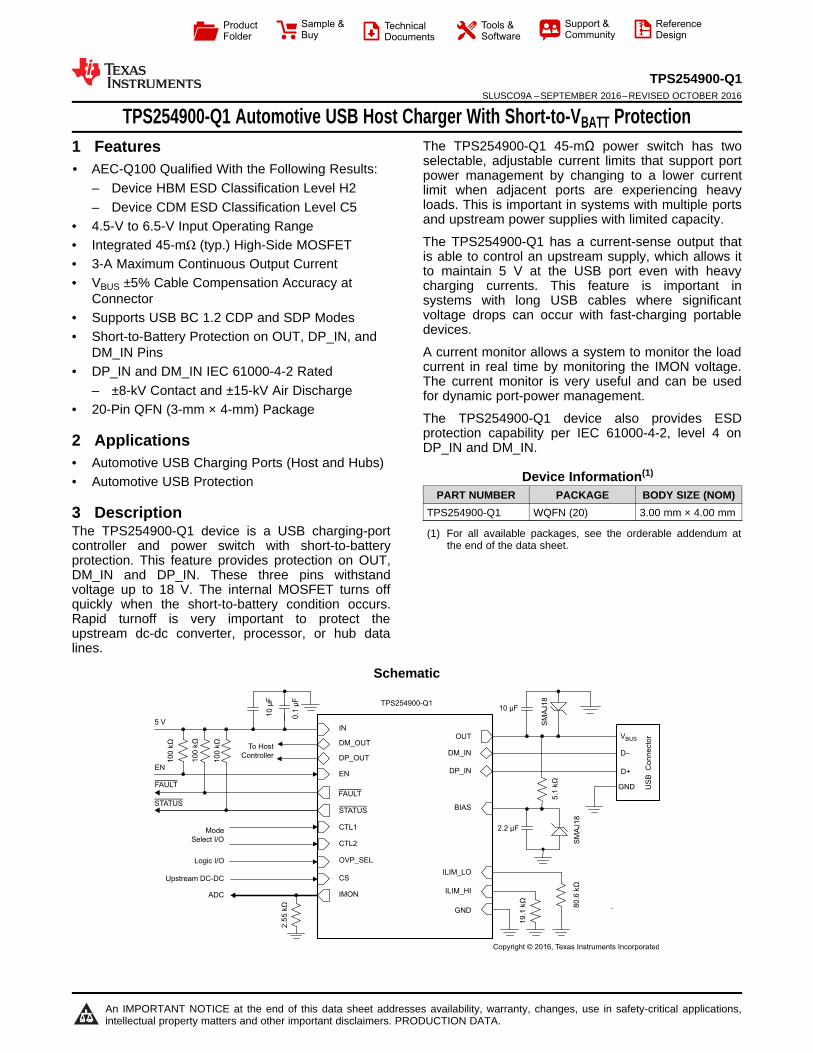
IN OUT DP_IN DM_IN ILIM_LO ILIM_HI GND CTL1 CTL2 CS EN TPS254900-Q1 5V EN FAULT FAULT STATUS STATUS 0.1 μF USB Connector Mode Select I/O V BUS D+ D– GND ADC Upstream DC-DC DP_OUT DM_OUT IMON OVP_SEL Logic I/O 10 F μ BIAS 2.2 μF 5.1 k Ω SMAJ18 100 k Ω 100 k Ω 100 k Ω 2.55 k Ω 19.1 k Ω 80.6 k Ω 10 F μ SMAJ18 To Host Controller Copyright © 2016, Texas Instruments Incorporated Product Folder Sample & Buy Technical Documents Tools & Software Support & Community Reference Design An IMPORTANT NOTICE at the end of this data sheet addresses availability, warranty, changes, use in safety-critical applications, intellectual property matters and other important disclaimers. PRODUCTION DATA. TPS254900-Q1 SLUSCO9A – SEPTEMBER 2016 – REVISED OCTOBER 2016 TPS254900-Q1 Automotive USB Host Charger With Short-to-V BATT Protection 1 1 Features 1• AEC-Q100 Qualified With the Following Results: – Device HBM ESD Classification Level H2 – Device CDM ESD Classification Level C5 • 4.5-V to 6.5-V Input Operating Range • Integrated 45-mΩ (typ.) High-Side MOSFET • 3-A Maximum Continuous Output Current • V BUS ±5% Cable Compensation Accuracy at Connector • Supports USB BC 1.2 CDP and SDP Modes • Short-to-Battery Protection on OUT, DP_IN, and DM_IN Pins • DP_IN and DM_IN IEC 61000-4-2 Rated – ±8-kV Contact and ±15-kV Air Discharge • 20-Pin QFN (3-mm × 4-mm) Package 2 Applications • Automotive USB Charging Ports (Host and Hubs) • Automotive USB Protection 3 Description The TPS254900-Q1 device is a USB charging-port controller and power switch with short-to-battery protection. This feature provides protection on OUT, DM_IN and DP_IN. These three pins withstand voltage up to 18 V. The internal MOSFET turns off quickly when the short-to-battery condition occurs. Rapid turnoff is very important to protect the upstream dc-dc converter, processor, or hub data lines. The TPS254900-Q1 45-mΩ power switch has two selectable, adjustable current limits that support port power management by changing to a lower current limit when adjacent ports are experiencing heavy loads. This is important in systems with multiple ports and upstream power supplies with limited capacity. The TPS254900-Q1 has a current-sense output that is able to control an upstream supply, which allows it to maintain 5 V at the USB port even with heavy charging currents. This feature is important in systems with long USB cables where significant voltage drops can occur with fast-charging portable devices. A current monitor allows a system to monitor the load current in real time by monitoring the IMON voltage. The current monitor is very useful and can be used for dynamic port-power management. The TPS254900-Q1 device also provides ESD protection capability per IEC 61000-4-2, level 4 on DP_IN and DM_IN. Device Information (1) PART NUMBER PACKAGE BODY SIZE (NOM) TPS254900-Q1 WQFN (20) 3.00 mm × 4.00 mm (1) For all available packages, see the orderable addendum at the end of the data sheet. Schematic
Transcript of TPS254900-Q1 Datasheet - Texas Instruments · in out dp_in dm_in ilim_lo ilim_hi gnd ctl1 ctl2 cs...
INOUT
DP_IN
DM_IN
ILIM_LO
ILIM_HI
GND
CTL1
CTL2
CS
EN
TPS254900-Q1
5 V
EN
FAULT
FAULT
STATUSSTATUS
0.1
µF
US
BC
on
ne
cto
r
Mode
Select I/O
VBUS
D+
D–
GND
ADC
Upstream DC-DC
DP_OUT
DM_OUT
IMON
OVP_SELLogic I/O
10
Fµ
BIAS
2.2 µF
5.1
kΩ
SM
AJ1
8
100
kΩ
10
0kΩ
10
0kΩ
2.5
5kΩ
19
.1kΩ
80.6
kΩ
10 Fµ
SM
AJ1
8
To Host
Controller
Copyright © 2016, Texas Instruments Incorporated
Product
Folder
Sample &Buy
Technical
Documents
Tools &
Software
Support &Community
ReferenceDesign
An IMPORTANT NOTICE at the end of this data sheet addresses availability, warranty, changes, use in safety-critical applications,intellectual property matters and other important disclaimers. PRODUCTION DATA.
TPS254900-Q1SLUSCO9A –SEPTEMBER 2016–REVISED OCTOBER 2016
TPS254900-Q1 Automotive USB Host Charger With Short-to-VBATT Protection
1
1 Features1• AEC-Q100 Qualified With the Following Results:
– Device HBM ESD Classification Level H2– Device CDM ESD Classification Level C5
• 4.5-V to 6.5-V Input Operating Range• Integrated 45-mΩ (typ.) High-Side MOSFET• 3-A Maximum Continuous Output Current• VBUS ±5% Cable Compensation Accuracy at
Connector• Supports USB BC 1.2 CDP and SDP Modes• Short-to-Battery Protection on OUT, DP_IN, and
DM_IN Pins• DP_IN and DM_IN IEC 61000-4-2 Rated
– ±8-kV Contact and ±15-kV Air Discharge• 20-Pin QFN (3-mm × 4-mm) Package
2 Applications• Automotive USB Charging Ports (Host and Hubs)• Automotive USB Protection
3 DescriptionThe TPS254900-Q1 device is a USB charging-portcontroller and power switch with short-to-batteryprotection. This feature provides protection on OUT,DM_IN and DP_IN. These three pins withstandvoltage up to 18 V. The internal MOSFET turns offquickly when the short-to-battery condition occurs.Rapid turnoff is very important to protect theupstream dc-dc converter, processor, or hub datalines.
The TPS254900-Q1 45-mΩ power switch has twoselectable, adjustable current limits that support portpower management by changing to a lower currentlimit when adjacent ports are experiencing heavyloads. This is important in systems with multiple portsand upstream power supplies with limited capacity.
The TPS254900-Q1 has a current-sense output thatis able to control an upstream supply, which allows itto maintain 5 V at the USB port even with heavycharging currents. This feature is important insystems with long USB cables where significantvoltage drops can occur with fast-charging portabledevices.
A current monitor allows a system to monitor the loadcurrent in real time by monitoring the IMON voltage.The current monitor is very useful and can be usedfor dynamic port-power management.
The TPS254900-Q1 device also provides ESDprotection capability per IEC 61000-4-2, level 4 onDP_IN and DM_IN.
Device Information(1)
PART NUMBER PACKAGE BODY SIZE (NOM)TPS254900-Q1 WQFN (20) 3.00 mm × 4.00 mm
(1) For all available packages, see the orderable addendum atthe end of the data sheet.
Schematic
2
TPS254900-Q1SLUSCO9A –SEPTEMBER 2016–REVISED OCTOBER 2016 www.ti.com
Product Folder Links: TPS254900-Q1
Submit Documentation Feedback Copyright © 2016, Texas Instruments Incorporated
Table of Contents1 Features .................................................................. 12 Applications ........................................................... 13 Description ............................................................. 14 Revision History..................................................... 25 Pin Configuration and Functions ......................... 36 Specifications......................................................... 4
6.1 Absolute Maximum Ratings ...................................... 46.2 ESD Ratings.............................................................. 46.3 Recommended Operating Conditions....................... 46.4 Thermal Information .................................................. 56.5 Electrical Characteristics........................................... 56.6 Switching Characteristics .......................................... 86.7 Typical Characteristics .............................................. 8
7 Parameter Measurement Information ................ 158 Detailed Description ............................................ 16
8.1 Overview ................................................................. 168.2 Functional Block Diagram ....................................... 178.3 Feature Description................................................. 17
8.4 Device Functional Modes........................................ 239 Application and Implementation ........................ 26
9.1 Application Information............................................ 269.2 Typical Application ................................................. 26
10 Power Supply Recommendations ..................... 3011 Layout................................................................... 30
11.1 Layout Guidelines ................................................. 3011.2 Layout Example .................................................... 32
12 Device and Documentation Support ................. 3312.1 Device Support...................................................... 3312.2 Documentation Support ........................................ 3312.3 Receiving Notification of Documentation Updates 3312.4 Community Resources.......................................... 3312.5 Trademarks ........................................................... 3312.6 Electrostatic Discharge Caution............................ 3312.7 Glossary ................................................................ 33
13 Mechanical, Packaging, and OrderableInformation ........................................................... 33
4 Revision History
Changes from Original (September 2016) to Revision A Page
• Changed data sheet from PRODUCT PREVIEW to PRODUCTION DATA .......................................................................... 1
Thermal
Pad
1IMON
2IN
3IN
4DM_OUT
5DP_OUT
6CS
7E
N
8C
TL1
9C
TL2
10O
VP
_SE
L
11 GND
12 BIAS
13 DP_IN
14 DM_IN
15 OUT
16 OUT
17S
TA
TU
S
18F
AU
LT
19IL
IM_L
O
20IL
IM_H
INot to scale
3
TPS254900-Q1www.ti.com SLUSCO9A –SEPTEMBER 2016–REVISED OCTOBER 2016
Product Folder Links: TPS254900-Q1
Submit Documentation FeedbackCopyright © 2016, Texas Instruments Incorporated
(1) I = Input, O = Output, I/O = Input and output, PWR = Power
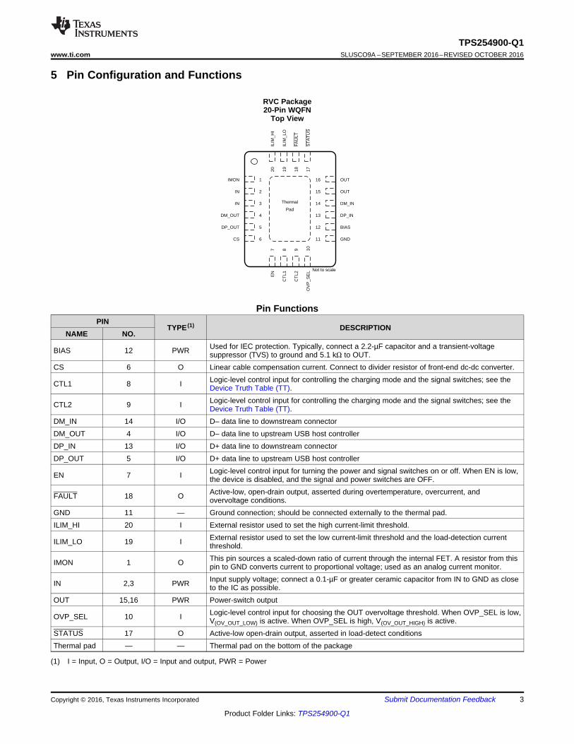
5 Pin Configuration and Functions
RVC Package20-Pin WQFN
Top View
Pin FunctionsPIN
TYPE (1) DESCRIPTIONNAME NO.
BIAS 12 PWR Used for IEC protection. Typically, connect a 2.2-µF capacitor and a transient-voltagesuppressor (TVS) to ground and 5.1 kΩ to OUT.
CS 6 O Linear cable compensation current. Connect to divider resistor of front-end dc-dc converter.
CTL1 8 I Logic-level control input for controlling the charging mode and the signal switches; see theDevice Truth Table (TT).
CTL2 9 I Logic-level control input for controlling the charging mode and the signal switches; see theDevice Truth Table (TT).
DM_IN 14 I/O D– data line to downstream connectorDM_OUT 4 I/O D– data line to upstream USB host controllerDP_IN 13 I/O D+ data line to downstream connectorDP_OUT 5 I/O D+ data line to upstream USB host controller
EN 7 I Logic-level control input for turning the power and signal switches on or off. When EN is low,the device is disabled, and the signal and power switches are OFF.
FAULT 18 O Active-low, open-drain output, asserted during overtemperature, overcurrent, andovervoltage conditions.
GND 11 — Ground connection; should be connected externally to the thermal pad.ILIM_HI 20 I External resistor used to set the high current-limit threshold.
ILIM_LO 19 I External resistor used to set the low current-limit threshold and the load-detection currentthreshold.
IMON 1 O This pin sources a scaled-down ratio of current through the internal FET. A resistor from thispin to GND converts current to proportional voltage; used as an analog current monitor.
IN 2,3 PWR Input supply voltage; connect a 0.1-µF or greater ceramic capacitor from IN to GND as closeto the IC as possible.
OUT 15,16 PWR Power-switch output
OVP_SEL 10 I Logic-level control input for choosing the OUT overvoltage threshold. When OVP_SEL is low,V(OV_OUT_LOW) is active. When OVP_SEL is high, V(OV_OUT_HIGH) is active.
STATUS 17 O Active-low open-drain output, asserted in load-detect conditionsThermal pad — — Thermal pad on the bottom of the package
4
TPS254900-Q1SLUSCO9A –SEPTEMBER 2016–REVISED OCTOBER 2016 www.ti.com
Product Folder Links: TPS254900-Q1
Submit Documentation Feedback Copyright © 2016, Texas Instruments Incorporated
(1) Stresses beyond those listed under Absolute Maximum Ratings may cause permanent damage to the device. These are stress ratingsonly, which do not imply functional operation of the device at these or any other conditions beyond those indicated under RecommendedOperating Conditions. Exposure to absolute-maximum-rated conditions for extended periods may affect device reliability.
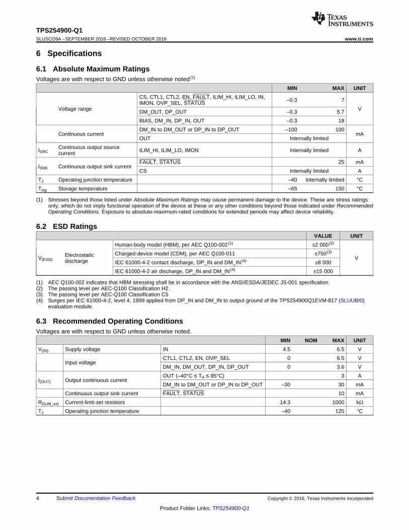
6 Specifications
6.1 Absolute Maximum RatingsVoltages are with respect to GND unless otherwise noted (1)
MIN MAX UNIT
Voltage range
CS, CTL1, CTL2, EN, FAULT, ILIM_HI, ILIM_LO, IN,IMON, OVP_SEL, STATUS –0.3 7
VDM_OUT, DP_OUT –0.3 5.7BIAS, DM_IN, DP_IN, OUT –0.3 18
Continuous currentDM_IN to DM_OUT or DP_IN to DP_OUT –100 100
mAOUT Internally limited
ISRCContinuous output sourcecurrent ILIM_HI, ILIM_LO, IMON Internally limited A
ISNK Continuous output sink currentFAULT, STATUS 25 mACS Internally limited A
TJ Operating junction temperature –40 Internally limited °CTstg Storage temperature –65 150 °C
(1) AEC Q100-002 indicates that HBM stressing shall be in accordance with the ANSI/ESDA/JEDEC JS-001 specification.(2) The passing level per AEC-Q100 Classification H2.(3) The passing level per AEC-Q100 Classification C5(4) Surges per IEC 61000-4-2, level 4, 1999 applied from DP_IN and DM_IN to output ground of the TPS254900Q1EVM-817 (SLUUBI0)
evaluation module.
6.2 ESD RatingsVALUE UNIT
V(ESD)Electrostaticdischarge
Human-body model (HBM), per AEC Q100-002 (1) ±2 000 (2)
VCharged-device model (CDM), per AEC Q100-011 ±750 (3)
IEC 61000-4-2 contact discharge, DP_IN and DM_IN (4) ±8 000IEC 61000-4-2 air discharge, DP_IN and DM_IN (4) ±15 000
6.3 Recommended Operating ConditionsVoltages are with respect to GND unless otherwise noted.
MIN NOM MAX UNITV(IN) Supply voltage IN 4.5 6.5 V
Input voltageCTL1, CTL2, EN, OVP_SEL 0 6.5 VDM_IN, DM_OUT, DP_IN, DP_OUT 0 3.6 V
I(OUT) Output continuous currentOUT (–40°C ≤ TA ≤ 85°C) 3 ADM_IN to DM_OUT or DP_IN to DP_OUT –30 30 mA
Continuous output sink current FAULT, STATUS 10 mAR(ILIM_xx) Current-limit-set resistors 14.3 1000 kΩTJ Operating junction temperature –40 125 °C
5
TPS254900-Q1www.ti.com SLUSCO9A –SEPTEMBER 2016–REVISED OCTOBER 2016
Product Folder Links: TPS254900-Q1
Submit Documentation FeedbackCopyright © 2016, Texas Instruments Incorporated
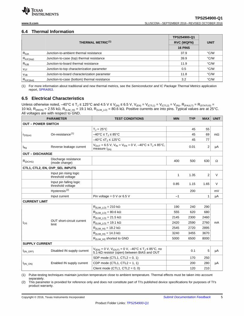
(1) For more information about traditional and new thermal metrics, see the Semiconductor and IC Package Thermal Metrics applicationreport, SPRA953.
6.4 Thermal Information
THERMAL METRIC (1)TPS254900-Q1
UNITRVC (WQFN)16 PINS
RθJA Junction-to-ambient thermal resistance 37.9 °C/WRθJC(top) Junction-to-case (top) thermal resistance 39.9 °C/WRθJB Junction-to-board thermal resistance 11.9 °C/WψJT Junction-to-top characterization parameter 0.5 °C/WψJB Junction-to-board characterization parameter 11.8 °C/WRθJC(bot) Junction-to-case (bottom) thermal resistance 3.2 °C/W
(1) Pulse-testing techniques maintain junction temperature close to ambient temperature. Thermal effects must be taken into accountseparately.
(2) This parameter is provided for reference only and does not constitute part of TI's published device specifications for purposes of TI'sproduct warranty.
6.5 Electrical CharacteristicsUnless otherwise noted, –40°C ≤ TJ ≤ 125°C and 4.5 V ≤ V(IN) ≤ 6.5 V, V(EN) = V(CTL1) = V(CTL2) = V(IN), R(FAULT) = R(STATUS) =10 kΩ, R(IMON) = 2.55 kΩ, R(ILIM_HI) = 19.1 kΩ, R(ILIM_LO) = 80.6 kΩ. Positive currents are into pins. Typical values are at 25°C.All voltages are with respect to GND.
PARAMETER TEST CONDITIONS MIN TYP MAX UNITOUT – POWER SWITCH
rDS(on) On-resistance (1)
TJ = 25°C 45 55mΩ–40°C ≤ TJ ≤ 85°C 45 69
–40°C ≤TJ ≤ 125°C 45 77
Ilkg Reverse leakage current VOUT = 6.5 V, VIN = VEN = 0 V, –40°C ≤ TJ ≤ 85°C,measure I(IN)
0.01 2 µA
OUT – DISCHARGE
R(DCHG)Discharge resistance(mode change) 400 500 630 Ω
CTL1, CTL2, EN, OVP_SEL INPUTSInput pin rising logicthreshold voltage 1 1.35 2 V
Input pin falling logicthreshold voltage 0.85 1.15 1.65 V
Hysteresis (2) 200 mVInput current Pin voltage = 0 V or 6.5 V –1 1 µA
CURRENT LIMIT
IOSOUT short-circuit currentlimit
R(ILIM_LO) = 210 kΩ 190 240 290
mA
R(ILIM_LO) = 80.6 kΩ 555 620 680R(ILIM_LO) = 21.5 kΩ 2145 2300 2460R(ILIM_LO) = 19.1 kΩ 2420 2590 2760R(ILIM_HI) = 18.2 kΩ 2545 2720 2895R(ILIM_HI) = 14.3 kΩ 3240 3455 3670R(ILIM_HI) shorted to GND 5000 6500 8000
SUPPLY CURRENT
I(IN_OFF) Disabled IN supply current V(EN) = 0 V, V(OUT) = 0 V, –40°C ≤ TJ ≤ 85°C, no5.1-kΩ resistor (open) between BIAS and OUT 0.1 5 µA
I(IN_ON) Enabled IN supply currentSDP mode (CTL1, CTL2 = 0, 1) 170 250
µACDP mode (CTL1, CTL2 = 1, 1) 200 280Client mode (CTL1, CTL2 = 0, 0) 120 210
6
TPS254900-Q1SLUSCO9A –SEPTEMBER 2016–REVISED OCTOBER 2016 www.ti.com
Product Folder Links: TPS254900-Q1
Submit Documentation Feedback Copyright © 2016, Texas Instruments Incorporated
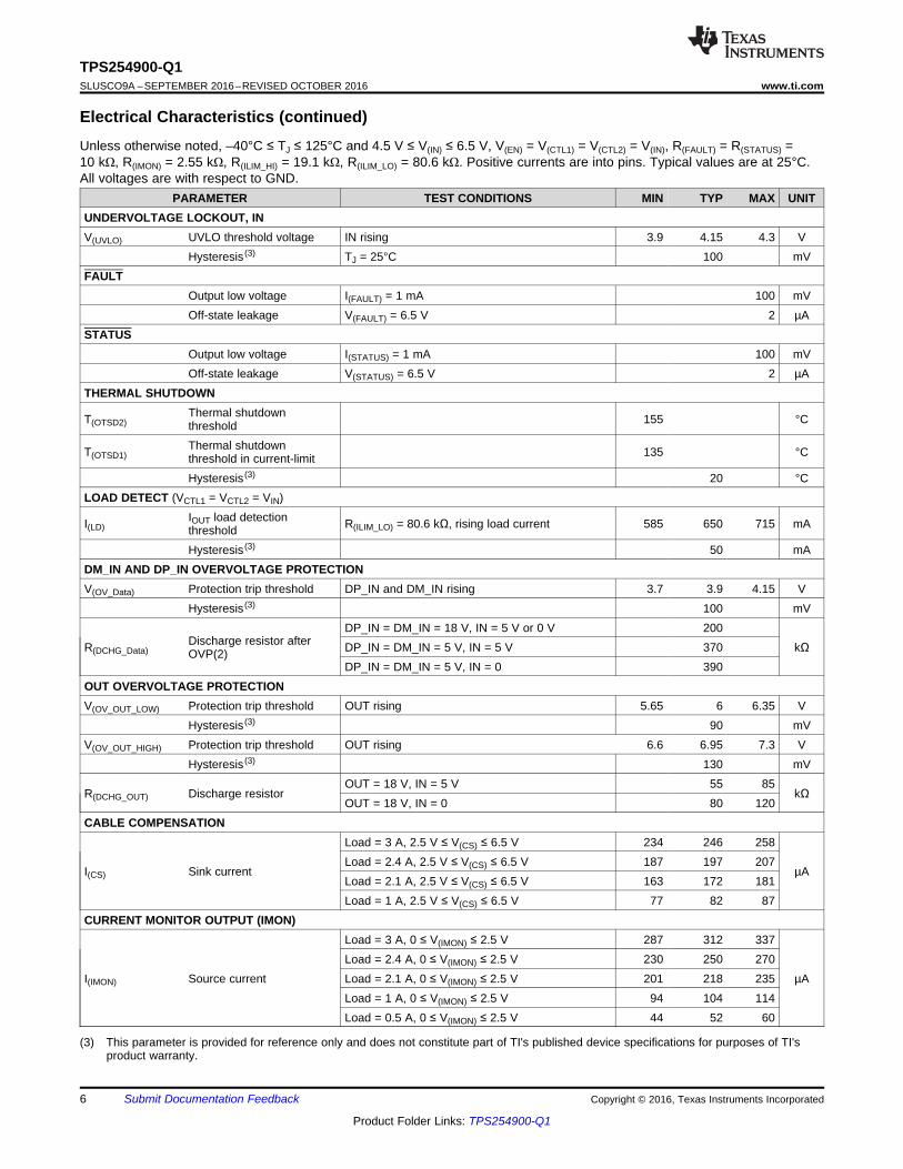
Electrical Characteristics (continued)Unless otherwise noted, –40°C ≤ TJ ≤ 125°C and 4.5 V ≤ V(IN) ≤ 6.5 V, V(EN) = V(CTL1) = V(CTL2) = V(IN), R(FAULT) = R(STATUS) =10 kΩ, R(IMON) = 2.55 kΩ, R(ILIM_HI) = 19.1 kΩ, R(ILIM_LO) = 80.6 kΩ. Positive currents are into pins. Typical values are at 25°C.All voltages are with respect to GND.
PARAMETER TEST CONDITIONS MIN TYP MAX UNIT
(3) This parameter is provided for reference only and does not constitute part of TI's published device specifications for purposes of TI'sproduct warranty.
UNDERVOLTAGE LOCKOUT, INV(UVLO) UVLO threshold voltage IN rising 3.9 4.15 4.3 V
Hysteresis (3) TJ = 25°C 100 mVFAULT
Output low voltage I(FAULT) = 1 mA 100 mVOff-state leakage V(FAULT) = 6.5 V 2 µA
STATUSOutput low voltage I(STATUS) = 1 mA 100 mVOff-state leakage V(STATUS) = 6.5 V 2 µA
THERMAL SHUTDOWN
T(OTSD2)Thermal shutdownthreshold 155 °C
T(OTSD1)Thermal shutdownthreshold in current-limit 135 °C
Hysteresis (3) 20 °CLOAD DETECT (VCTL1 = VCTL2 = VIN)
I(LD)IOUT load detectionthreshold R(ILIM_LO) = 80.6 kΩ, rising load current 585 650 715 mA
Hysteresis (3) 50 mADM_IN AND DP_IN OVERVOLTAGE PROTECTIONV(OV_Data) Protection trip threshold DP_IN and DM_IN rising 3.7 3.9 4.15 V
Hysteresis (3) 100 mV
R(DCHG_Data)Discharge resistor afterOVP(2)
DP_IN = DM_IN = 18 V, IN = 5 V or 0 V 200kΩDP_IN = DM_IN = 5 V, IN = 5 V 370
DP_IN = DM_IN = 5 V, IN = 0 390OUT OVERVOLTAGE PROTECTIONV(OV_OUT_LOW) Protection trip threshold OUT rising 5.65 6 6.35 V
Hysteresis (3) 90 mVV(OV_OUT_HIGH) Protection trip threshold OUT rising 6.6 6.95 7.3 V
Hysteresis (3) 130 mV
R(DCHG_OUT) Discharge resistorOUT = 18 V, IN = 5 V 55 85
kΩOUT = 18 V, IN = 0 80 120
CABLE COMPENSATION
I(CS) Sink current
Load = 3 A, 2.5 V ≤ V(CS) ≤ 6.5 V 234 246 258
µALoad = 2.4 A, 2.5 V ≤ V(CS) ≤ 6.5 V 187 197 207Load = 2.1 A, 2.5 V ≤ V(CS) ≤ 6.5 V 163 172 181Load = 1 A, 2.5 V ≤ V(CS) ≤ 6.5 V 77 82 87
CURRENT MONITOR OUTPUT (IMON)
I(IMON) Source current
Load = 3 A, 0 ≤ V(IMON) ≤ 2.5 V 287 312 337
µALoad = 2.4 A, 0 ≤ V(IMON) ≤ 2.5 V 230 250 270Load = 2.1 A, 0 ≤ V(IMON) ≤ 2.5 V 201 218 235Load = 1 A, 0 ≤ V(IMON) ≤ 2.5 V 94 104 114Load = 0.5 A, 0 ≤ V(IMON) ≤ 2.5 V 44 52 60
7
TPS254900-Q1www.ti.com SLUSCO9A –SEPTEMBER 2016–REVISED OCTOBER 2016
Product Folder Links: TPS254900-Q1
Submit Documentation FeedbackCopyright © 2016, Texas Instruments Incorporated
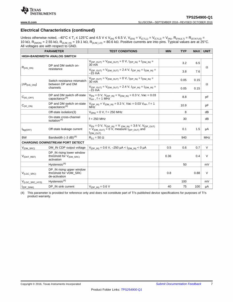
Electrical Characteristics (continued)Unless otherwise noted, –40°C ≤ TJ ≤ 125°C and 4.5 V ≤ V(IN) ≤ 6.5 V, V(EN) = V(CTL1) = V(CTL2) = V(IN), R(FAULT) = R(STATUS) =10 kΩ, R(IMON) = 2.55 kΩ, R(ILIM_HI) = 19.1 kΩ, R(ILIM_LO) = 80.6 kΩ. Positive currents are into pins. Typical values are at 25°C.All voltages are with respect to GND.
PARAMETER TEST CONDITIONS MIN TYP MAX UNIT
(4) This parameter is provided for reference only and does not constitute part of TI's published device specifications for purposes of TI'sproduct warranty.
HIGH-BANDWIDTH ANALOG SWITCH
R(HS_ON)DP and DM switch on-resistance
V(DP_OUT) = V(DM_OUT) = 0 V, I(DP_IN) = I(DM_IN) =30 mA 3.2 6.5
ΩV(DP_OUT) = V(DM_OUT) = 2.4 V, I(DP_IN) = I(DM_IN) =–15 mA 3.8 7.6
|ΔR(HS_ON)|Switch resistance mismatchbetween DP and DMchannels
V(DP_OUT) = V(DM_OUT) = 0 V, I(DP_IN) = I(DM_IN) =30 mA 0.05 0.15
ΩV(DP_OUT) = V(DM_OUT) = 2.4 V, I(DP_IN) = I(DM_IN) =–15 mA 0.05 0.15
C(IO_OFF)DP and DM switch off-statecapacitance (4)
VEN = 0 V, V(DP_IN) = V(DM_IN) = 0.3 V, Vac = 0.03VPP , f = 1 MHz 8.8 pF
C(IO_ON)DP and DM switch on-statecapacitance (4)
V(DP_IN) = V(DM_IN) = 0.3 V, Vac = 0.03 VPP, f = 1MHz 10.9 pF
Off-state isolation(3) V(EN) = 0 V, f = 250 MHz 8 dBOn-state cross-channelisolation (4) f = 250 MHz 30 dB
Ilkg(OFF) Off-state leakage currentVEN = 0 V, V(DP_IN) = V (DM_IN) = 3.6 V, V(DP_OUT)= V(DM_OUT) = 0 V, measure I(DP_OUT) andI(DM_OUT)
0.1 1.5 µA
BW Bandwidth (–3 dB) (4) R(L) = 50 Ω 940 MHzCHARGING DOWNSTREAM PORT DETECTV(DM_SRC) DM_IN CDP output voltage V(DP_IN) = 0.6 V, –250 µA < I(DM_IN) < 0 µA 0.5 0.6 0.7 V
V(DAT_REF)
DP_IN rising lower windowthreshold for V(DM_SRC)activation
0.36 0.4 V
Hysteresis (4) 50 mV
V(LGC_SRC)
DP_IN rising upper windowthreshold for VDM_SRCde-activation
0.8 0.88 V
V(LGC_SRC_HYS) Hysteresis (4) 100 mVI(DP_SINK) DP_IN sink current V(DP_IN) = 0.6 V 40 75 100 µA
Junction Temperature (qC)
Pow
er S
witc
h O
n R
esis
tanc
e (m:
)
-40 -25 -10 5 20 35 50 65 80 95 110 12530
35
40
45
50
55
60
65
70
D001Junction Temperature (qC)
OU
T R
ever
se L
eaka
ge C
urre
nt (P
A)
-40 -25 -10 5 20 35 50 65 80 95 110 12539.6
39.8
40
40.2
40.4
40.6
40.8
41
D002
8
TPS254900-Q1SLUSCO9A –SEPTEMBER 2016–REVISED OCTOBER 2016 www.ti.com
Product Folder Links: TPS254900-Q1
Submit Documentation Feedback Copyright © 2016, Texas Instruments Incorporated
(1) These parameters are provided for reference only and do not constitute part of TI's published device specifications for purposes of TI'sproduct warranty.
6.6 Switching CharacteristicsUnless otherwise noted –40°C ≤ TJ ≤ 125°C and 4.5 V ≤ V(IN) ≤ 6.5 V, V(EN) = V(IN), V(CTL1) = V(CTL2) = V(IN). R(FAULT) = R(STATUS)= 10 kΩ, R(IMON) = 2.55 KΩ, R(ILIM_HI) = 19.1 kΩ, R(ILIM_LO) = 80.6 kΩ. Positive currents are into pins. Typical values are at25°C. All voltages are with respect to GND.
PARAMETER TEST CONDITIONS MIN TYP MAX UNITtr OUT voltage rise time V(IN) = 5 V, C(L) = 1 µF, R(L) = 100 Ω 1.05 1.75 3.1 mstf OUT voltage fall time 0.27 0.47 0.82 mston OUT voltage turnon time V(IN) = 5 V, C(L) = 1 µF, R(L) = 100 Ω 7.5 11 mstoff OUT voltage turnoff time 2.7 5 mst(DCHG_S) Discharge hold time (mode
change)Time V(OUT) < 0.7 V 1.1 2 2.9 s
t(IOS) OUT short-circuit responsetime (1)
V(IN) = 5 V, R(SHORT) = 50 mΩ 2 µs
t(OC_OUT_FAULT) OUT FAULT deglitch time Bidirectional deglitch applicable to current-limitcondition only (no deglitch assertion for OTSD)
5.5 8.5 11.5 ms
tpd Analog switch propagationdelay (1)
V(IN) = 5 V 0.14 ns
t(SK) Analog switch skewbetween oppositetransitions of the same port(tPHL – tPLH) (1)
V(IN) = 5 V 0.02 ns
t(LD_SET) Load-detect set time V(IN) = 5 V 120 210 280 mst(LD_RESET) Load-detect reset time V(IN) = 5 V 1.8 3 4.2 st(OV_Data) DP_IN and DM_IN
overvoltage protectionresponse time
5 µs
t(OV_OUT) OUT overvoltage protectionresponse time
0.3 µs
t(OV_D_FAULT) DP_IN and DM_IN FAULT-asserted degltich time
11 16 23 ms
OUT FAULT-asserteddegltich time
11 16 23 ms
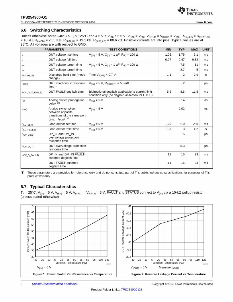
6.7 Typical CharacteristicsTA = 25°C, V(IN) = 5 V, V(EN) = 5 V, V(CTL1) = V(CTL2) = 5 V, FAULT and STATUS connect to V(IN) via a 10-kΩ pullup resistor(unless stated otherwise)
V(IN) = 5 V
Figure 1. Power Switch On-Resistance vs Temperature
V(OUT) = 5 V Measure I(OUT)
Figure 2. Reverse Leakage Current vs Temperature
Junction Temperature (qC)
IIN_O
FF
(P
A)
-40 -25 -10 5 20 35 50 65 80 95 110 125-2
0
2
4
6
D007
VIN = 4.5 VVIN = 5 VVIN = 6.5 V
Junction Temperature (qC)
IIN_O
N (P
A)
-40 -25 -10 5 20 35 50 65 80 95 110 125160
180
200
220
240
D008
VIN = 4.5 VVIN = 5 VVIN = 6.5 V
Junction Temperature (qC)
OU
T S
hort
Circ
uit L
imit
(mA
)
-40 -25 -10 5 20 35 50 65 80 95 110 1252000
2200
2400
2600
2800
3000
3200
3400
3600
D005
RILIM_HI = 21.5 KRILIM_HI = 19.1 K
RILIM_HI = 18.2 KRILIM_HI = 14.3 K
Junction Temperature (qC)
OU
T S
hort
Circ
uit L
imit
(mA
)
-40 -25 -10 5 20 35 50 65 80 95 110 1250
100
200
300
400
500
600
700
D006
RILIM_LO = 210 k:RILIM_LO = 80.6 k:
Junction Temperature (qC)
OU
T D
isch
arge
Res
ista
nce
(:)
-40 -25 -10 5 20 35 50 65 80 95 110 125480
490
500
510
520
530
540
550
560
570
D003
VIN = 4.5 VVIN = 5.0 VVIN = 6.5 V
Junction Temperature (qC)
OU
T D
isch
arge
Res
ista
nce
(:)
-40 -25 -10 5 20 35 50 65 80 95 110 12540
50
60
70
80
90
100
D004
VIN = 5 VVIN = 0 V
9
TPS254900-Q1www.ti.com SLUSCO9A –SEPTEMBER 2016–REVISED OCTOBER 2016
Product Folder Links: TPS254900-Q1
Submit Documentation FeedbackCopyright © 2016, Texas Instruments Incorporated
Typical Characteristics (continued)TA = 25°C, V(IN) = 5 V, V(EN) = 5 V, V(CTL1) = V(CTL2) = 5 V, FAULT and STATUS connect to V(IN) via a 10-kΩ pullup resistor(unless stated otherwise)
A
Figure 3. OUT Discharge Resistance (Mode Change) vsTemperature
A
Figure 4. OUT Discharge Resistance (OVP) vs Temperature
V(IN) = 5 V
Figure 5. OUT Short-Circuit Current Limit vs Temperature I
V(IN) = 5 V
Figure 6. OUT Short-Circuit Current Limit vs Temperature II
CTL1 = 1 CTL2 = 1
Figure 7. Disabled IN Supply Current vs Temperature
CTL1 = 1 CTL2 = 1
Figure 8. Enabled IN Supply Current – CDP (11) vsTemperature
Junction Temperature (qC)
I CS (P
A)
2.5 3 3.5 4 4.5 5 5.5 6 6.50
50
100
150
200
250
300
D017
IOUT = 1 AIOUT = 2.1 A
IOUT = 2.4 AIOUT = 3 A
Junction Temperature (qC)
I CS (P
A)
-40 -25 -10 5 20 35 50 65 80 95 110 125200
220
240
260
280
300
320
340
D018
IOUT = 2.1 A IOT = 2.4 A IOUT = 3 A
Junction Temperature (qC)
I CS (P
A)
-40 -25 -10 5 20 35 50 65 80 95 110 125 1400
50
100
150
200
250
300
D016
IOUT = 1 AIOUT = 2.1 A
IOUT = 2.4 AIOUT = 3 A
Junction Temperature (qC)
DP
_IN
Ove
r-vo
ltage
Pro
tect
ion
Thr
esho
ld (
V)
-40 -25 -10 5 20 35 50 65 80 95 110 1256.6
6.7
6.8
6.9
7
7.1
7.2
7.3
D014
Junction Temperature (qC)
Cur
rent
(P
A)
-40 -25 -10 5 20 35 50 65 80 95 110 125600
610
620
630
640
650
660
D011
LLD IOUT Rising Load Detect ThresholdIOS IOUT Short Circuit Current Limit
Junction Temperature (qC)
DP
_IN
Ove
r-vo
ltage
P
rote
ctio
n T
hres
hold
(V
)
-40 -25 -10 5 20 35 50 65 80 95 110 1253.6
3.7
3.8
3.9
4
4.1
4.2
D012
10
TPS254900-Q1SLUSCO9A –SEPTEMBER 2016–REVISED OCTOBER 2016 www.ti.com
Product Folder Links: TPS254900-Q1
Submit Documentation Feedback Copyright © 2016, Texas Instruments Incorporated
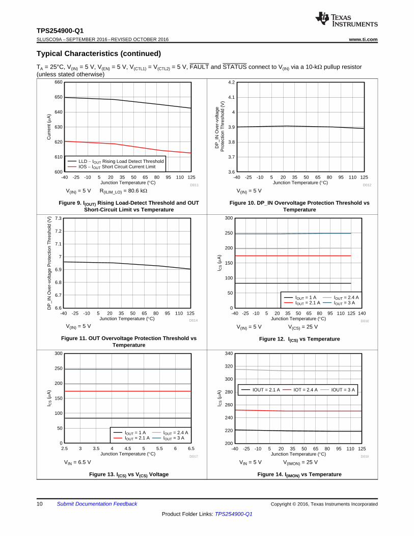
Typical Characteristics (continued)TA = 25°C, V(IN) = 5 V, V(EN) = 5 V, V(CTL1) = V(CTL2) = 5 V, FAULT and STATUS connect to V(IN) via a 10-kΩ pullup resistor(unless stated otherwise)
V(IN) = 5 V R(ILIM_LO) = 80.6 kΩ
Figure 9. I(OUT) Rising Load-Detect Threshold and OUTShort-Circuit Limit vs Temperature
V(IN) = 5 V
Figure 10. DP_IN Overvoltage Protection Threshold vsTemperature
V(IN) = 5 V
Figure 11. OUT Overvoltage Protection Threshold vsTemperature
V(IN) = 5 V V(CS) = 25 V
Figure 12. I(CS) vs Temperature
VIN = 6.5 V
Figure 13. I(CS) vs V(CS) Voltage
VIN = 5 V V(IMON) = 25 V
Figure 14. I(IMON) vs Temperature
VEN
5 V/div
VOUT
2 V/div
IOUT
0.5 A/div
VCS Voltage (V)
I CS (P
A)
0 0.5 1 1.5 2 2.5180
200
220
240
260
280
300
320
D020
IOUT = 2.1 AIOUT = 2.4 A
IOUT = 3 A
11
TPS254900-Q1www.ti.com SLUSCO9A –SEPTEMBER 2016–REVISED OCTOBER 2016
Product Folder Links: TPS254900-Q1
Submit Documentation FeedbackCopyright © 2016, Texas Instruments Incorporated
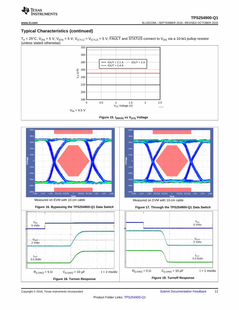
Typical Characteristics (continued)TA = 25°C, V(IN) = 5 V, V(EN) = 5 V, V(CTL1) = V(CTL2) = 5 V, FAULT and STATUS connect to V(IN) via a 10-kΩ pullup resistor(unless stated otherwise)
VIN = 4.5 V
Figure 15. I(IMON) vs V(CS) Voltage
Measured on EVM with 10-cm cable
Figure 16. Bypassing the TPS254900-Q1 Data Switch
Measured on EVM with 10-cm cable
Figure 17. Through the TPS254900-Q1 Data Switch
R(LOAD) = 5 Ω C(LOAD) = 10 µF t = 2 ms/div
Figure 18. Turnon Response
R(LOAD) = 5 Ω C(LOAD) = 10 µF t = 1 ms/div
Figure 19. Turnoff Response
12
TPS254900-Q1SLUSCO9A –SEPTEMBER 2016–REVISED OCTOBER 2016 www.ti.com
Product Folder Links: TPS254900-Q1
Submit Documentation Feedback Copyright © 2016, Texas Instruments Incorporated
Typical Characteristics (continued)TA = 25°C, V(IN) = 5 V, V(EN) = 5 V, V(CTL1) = V(CTL2) = 5 V, FAULT and STATUS connect to V(IN) via a 10-kΩ pullup resistor(unless stated otherwise)
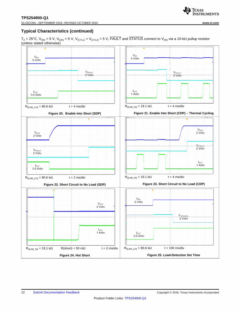
R(ILIM_LO) = 80.6 kΩ t = 4 ms/div
Figure 20. Enable Into Short (SDP)
R(ILIM_HI) = 19.1 kΩ t = 4 ms/div
Figure 21. Enable Into Short (CDP) – Thermal Cycling
R(ILIM_LO) = 80.6 kΩ t = 2 ms/div
Figure 22. Short Circuit to No Load (SDP)
R(ILIM_HI) = 19.1 kΩ t = 4 ms/div
Figure 23. Short Circuit to No Load (CDP)
R(ILIM_HI) = 19.1 kΩ R(short) = 50 mΩ t = 2 ms/div
Figure 24. Hot Short
R(ILIM_LO) = 80.6 kΩ t = 100 ms/div
Figure 25. Load-Detection Set Time
13
TPS254900-Q1www.ti.com SLUSCO9A –SEPTEMBER 2016–REVISED OCTOBER 2016
Product Folder Links: TPS254900-Q1
Submit Documentation FeedbackCopyright © 2016, Texas Instruments Incorporated
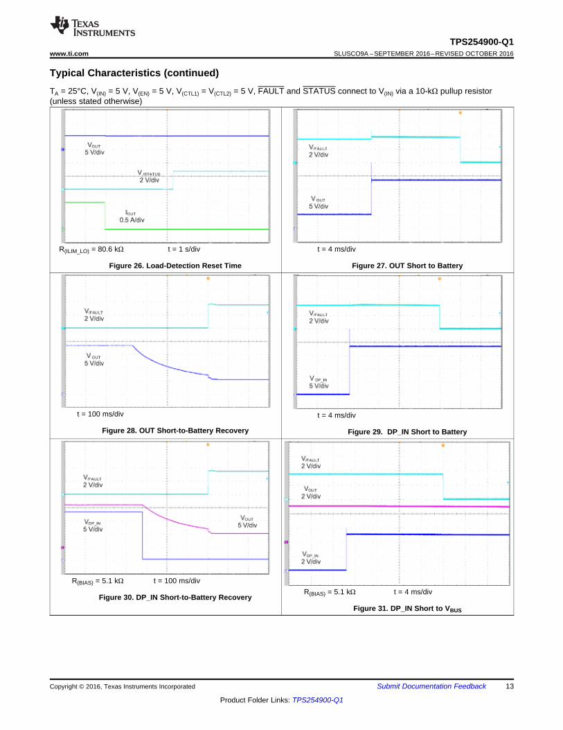
Typical Characteristics (continued)TA = 25°C, V(IN) = 5 V, V(EN) = 5 V, V(CTL1) = V(CTL2) = 5 V, FAULT and STATUS connect to V(IN) via a 10-kΩ pullup resistor(unless stated otherwise)
R(ILIM_LO) = 80.6 kΩ t = 1 s/div
Figure 26. Load-Detection Reset Time
t = 4 ms/div
Figure 27. OUT Short to Battery
t = 100 ms/div
Figure 28. OUT Short-to-Battery Recovery
t = 4 ms/div
Figure 29. DP_IN Short to Battery
R(BIAS) = 5.1 kΩ t = 100 ms/div
Figure 30. DP_IN Short-to-Battery RecoveryR(BIAS) = 5.1 kΩ t = 4 ms/div
Figure 31. DP_IN Short to VBUS
14
TPS254900-Q1SLUSCO9A –SEPTEMBER 2016–REVISED OCTOBER 2016 www.ti.com
Product Folder Links: TPS254900-Q1
Submit Documentation Feedback Copyright © 2016, Texas Instruments Incorporated
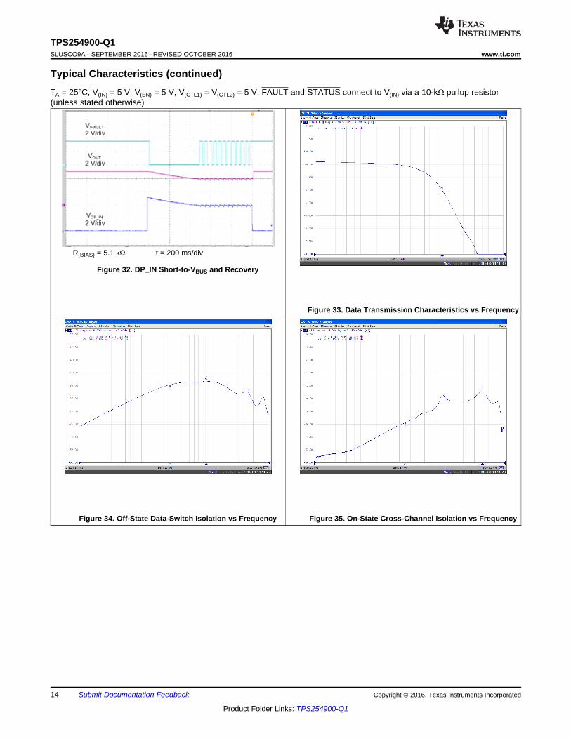
Typical Characteristics (continued)TA = 25°C, V(IN) = 5 V, V(EN) = 5 V, V(CTL1) = V(CTL2) = 5 V, FAULT and STATUS connect to V(IN) via a 10-kΩ pullup resistor(unless stated otherwise)
R(BIAS) = 5.1 kΩ t = 200 ms/div
Figure 32. DP_IN Short-to-VBUS and Recovery
Figure 33. Data Transmission Characteristics vs Frequency
Figure 34. Off-State Data-Switch Isolation vs Frequency Figure 35. On-State Cross-Channel Isolation vs Frequency
DC
Po
wer
Supply
LM
R1
40
30
TP
S254900-Q
1
PWR817A
27 mF
35 V
10 cm AWG18
Manually Hot-short 0.5 m AWG22
18 V
GND
5 VOUT
DP_IN
DM_IN
GND
0.5 m AWG28
0.5 m AWG28
I CA
BLE
Vo
ltag
eTe
st
Po
int
Copyright © 2016, Texas Instruments Incorporated
15
TPS254900-Q1www.ti.com SLUSCO9A –SEPTEMBER 2016–REVISED OCTOBER 2016
Product Folder Links: TPS254900-Q1
Submit Documentation FeedbackCopyright © 2016, Texas Instruments Incorporated
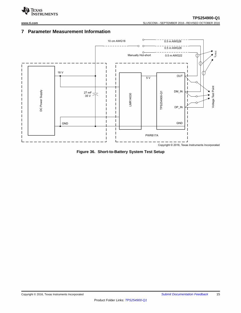
7 Parameter Measurement Information
Figure 36. Short-to-Battery System Test Setup
16
TPS254900-Q1SLUSCO9A –SEPTEMBER 2016–REVISED OCTOBER 2016 www.ti.com
Product Folder Links: TPS254900-Q1
Submit Documentation Feedback Copyright © 2016, Texas Instruments Incorporated
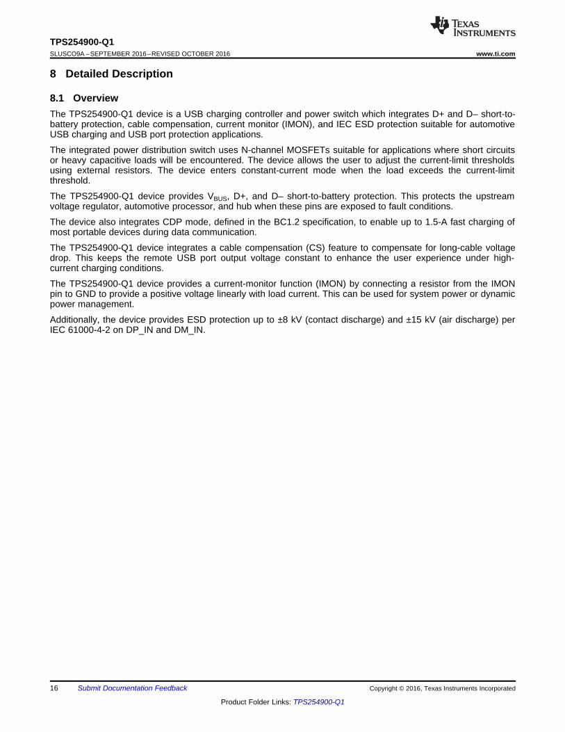
8 Detailed Description
8.1 OverviewThe TPS254900-Q1 device is a USB charging controller and power switch which integrates D+ and D– short-to-battery protection, cable compensation, current monitor (IMON), and IEC ESD protection suitable for automotiveUSB charging and USB port protection applications.
The integrated power distribution switch uses N-channel MOSFETs suitable for applications where short circuitsor heavy capacitive loads will be encountered. The device allows the user to adjust the current-limit thresholdsusing external resistors. The device enters constant-current mode when the load exceeds the current-limitthreshold.
The TPS254900-Q1 device provides VBUS, D+, and D– short-to-battery protection. This protects the upstreamvoltage regulator, automotive processor, and hub when these pins are exposed to fault conditions.
The device also integrates CDP mode, defined in the BC1.2 specification, to enable up to 1.5-A fast charging ofmost portable devices during data communication.
The TPS254900-Q1 device integrates a cable compensation (CS) feature to compensate for long-cable voltagedrop. This keeps the remote USB port output voltage constant to enhance the user experience under high-current charging conditions.
The TPS254900-Q1 device provides a current-monitor function (IMON) by connecting a resistor from the IMONpin to GND to provide a positive voltage linearly with load current. This can be used for system power or dynamicpower management.
Additionally, the device provides ESD protection up to ±8 kV (contact discharge) and ±15 kV (air discharge) perIEC 61000-4-2 on DP_IN and DM_IN.
IEC ESD
Protection
Disable + UVLO +
Discharge + OVP
Driver
CS
CurrentLimit
ChargePump
UVLO
Thermal
Sense
8-msDeglitch
OTSD
FAULT
CurrentSense
IN
EN
ILIM_HI
CS
DP_IN
DM_IN
OUT
GND
ILIM_LO
OC
STATUSLogic
Control
OVP2/3 (Short to BAT)
CDP
Detection
Discharge
DM_OUT
DP_OUT
CTL1
CTL2
OVP1
(Short to BAT)
IMON
´82 µA/A
´104 µA/A
OVP_SEL
BIAS
Copyright © 2016, Texas Instruments Incorporated
17
TPS254900-Q1www.ti.com SLUSCO9A –SEPTEMBER 2016–REVISED OCTOBER 2016
Product Folder Links: TPS254900-Q1
Submit Documentation FeedbackCopyright © 2016, Texas Instruments Incorporated
8.2 Functional Block Diagram
8.3 Feature Description
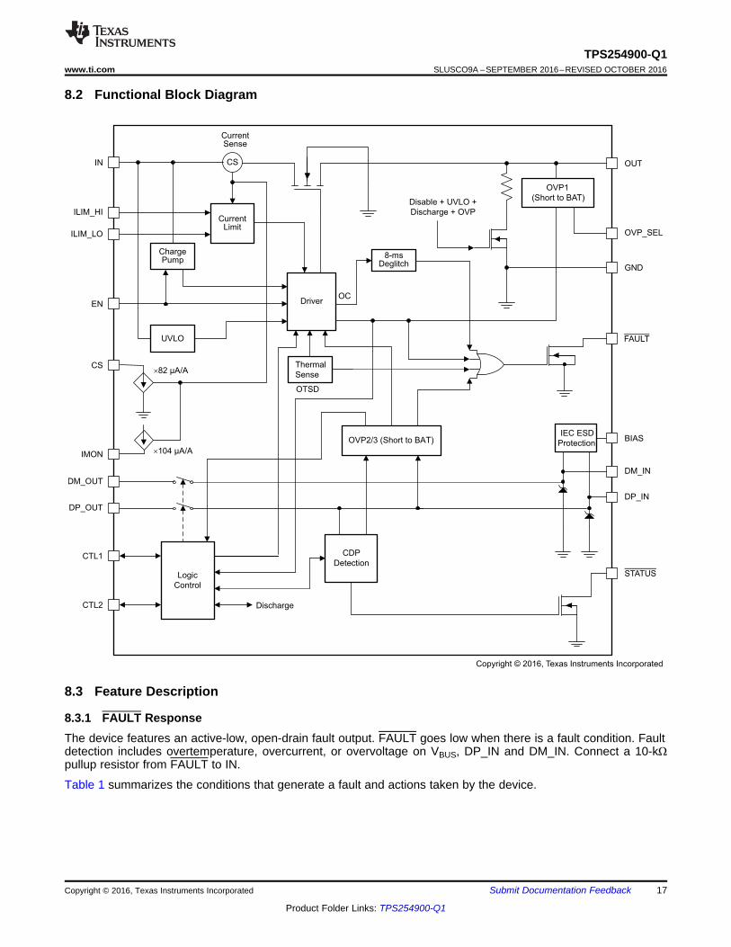
8.3.1 FAULT ResponseThe device features an active-low, open-drain fault output. FAULT goes low when there is a fault condition. Faultdetection includes overtemperature, overcurrent, or overvoltage on VBUS, DP_IN and DM_IN. Connect a 10-kΩpullup resistor from FAULT to IN.
Table 1 summarizes the conditions that generate a fault and actions taken by the device.
00.5
V(OUT) With Compensation
V(DROP)
5.x VBUS With Compensation
VBUS Without Compensation
V(O
UT
)(V
)
1 1.5 2 2.5 3I(OUT) (A)
18
TPS254900-Q1SLUSCO9A –SEPTEMBER 2016–REVISED OCTOBER 2016 www.ti.com
Product Folder Links: TPS254900-Q1
Submit Documentation Feedback Copyright © 2016, Texas Instruments Incorporated
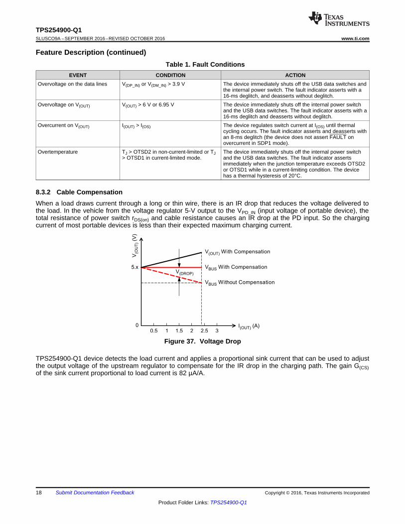
Feature Description (continued)Table 1. Fault Conditions
EVENT CONDITION ACTIONOvervoltage on the data lines V(DP_IN) or V(DM_IN) > 3.9 V The device immediately shuts off the USB data switches and
the internal power switch. The fault indicator asserts with a16-ms deglitch, and deasserts without deglitch.
Overvoltage on V(OUT) V(OUT) > 6 V or 6.95 V The device immediately shuts off the internal power switchand the USB data switches. The fault indicator asserts with a16-ms deglitch and deasserts without deglitch.
Overcurrent on V(OUT) I(OUT) > I(OS) The device regulates switch current at I(OS) until thermalcycling occurs. The fault indicator asserts and deasserts withan 8-ms deglitch (the device does not assert FAULT onovercurrent in SDP1 mode).
Overtemperature TJ > OTSD2 in non-current-limited or TJ> OTSD1 in current-limited mode.
The device immediately shuts off the internal power switchand the USB data switches. The fault indicator assertsimmediately when the junction temperature exceeds OTSD2or OTSD1 while in a current-limiting condition. The devicehas a thermal hysteresis of 20°C.
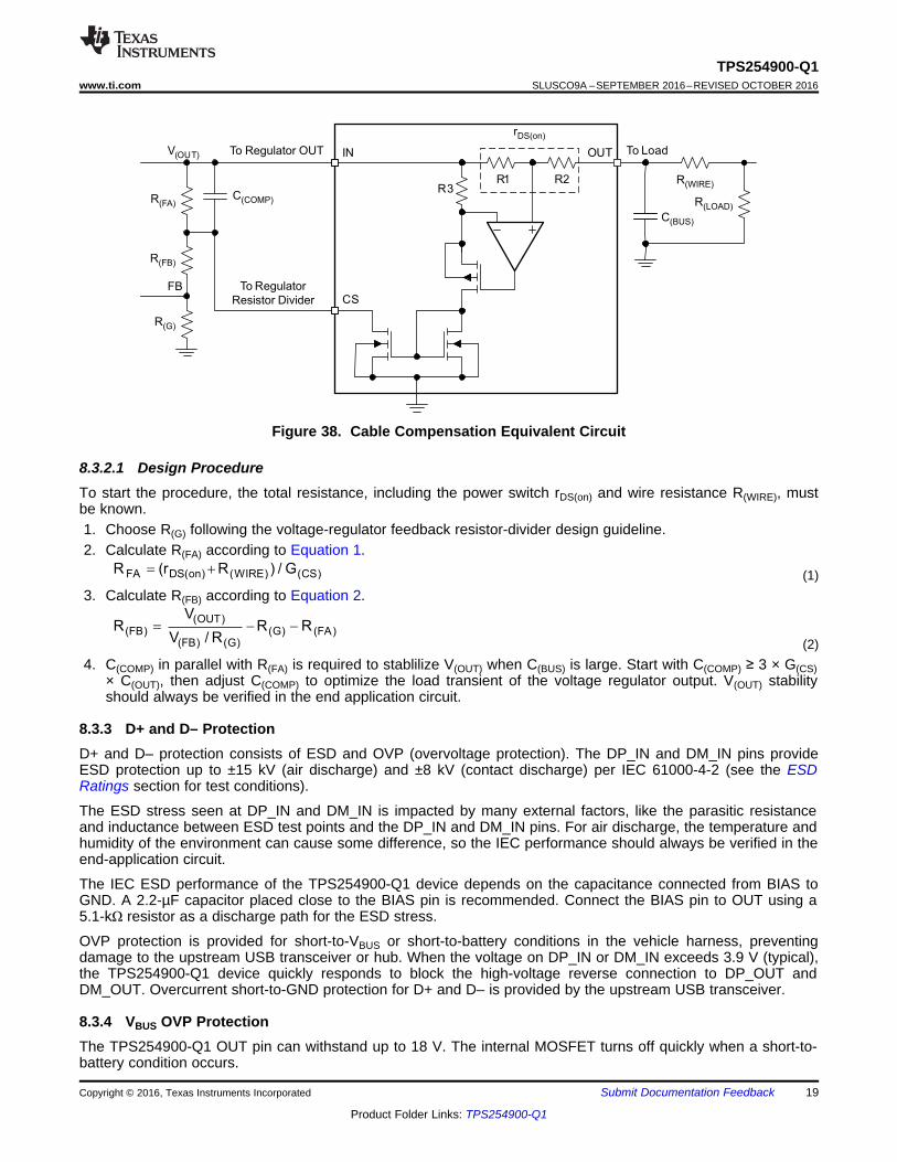
8.3.2 Cable CompensationWhen a load draws current through a long or thin wire, there is an IR drop that reduces the voltage delivered tothe load. In the vehicle from the voltage regulator 5-V output to the VPD_IN (input voltage of portable device), thetotal resistance of power switch rDS(on) and cable resistance causes an IR drop at the PD input. So the chargingcurrent of most portable devices is less than their expected maximum charging current.
Figure 37. Voltage Drop
TPS254900-Q1 device detects the load current and applies a proportional sink current that can be used to adjustthe output voltage of the upstream regulator to compensate for the IR drop in the charging path. The gain G(CS)of the sink current proportional to load current is 82 µA/A.
(OUT)(FB) (G) (FA)
(FB) (G)
VR R R
V / R= - -
FA DS(on) (WIRE) (CS)R (r R ) / G= +
IN OUT
CS
R1R3
To Regulator OUT To Load
To Regulator
Resistor Divider
V(OUT)
R(FA)
R(G)
R(FB)
FB
C(BUS)
R(WIRE)
R(LOAD)C(COMP)
rDS(on)
R2
19
TPS254900-Q1www.ti.com SLUSCO9A –SEPTEMBER 2016–REVISED OCTOBER 2016
Product Folder Links: TPS254900-Q1
Submit Documentation FeedbackCopyright © 2016, Texas Instruments Incorporated
Figure 38. Cable Compensation Equivalent Circuit
8.3.2.1 Design ProcedureTo start the procedure, the total resistance, including the power switch rDS(on) and wire resistance R(WIRE), mustbe known.1. Choose R(G) following the voltage-regulator feedback resistor-divider design guideline.2. Calculate R(FA) according to Equation 1.
(1)3. Calculate R(FB) according to Equation 2.
(2)4. C(COMP) in parallel with R(FA) is required to stablilize V(OUT) when C(BUS) is large. Start with C(COMP) ≥ 3 × G(CS)
× C(OUT), then adjust C(COMP) to optimize the load transient of the voltage regulator output. V(OUT) stabilityshould always be verified in the end application circuit.
8.3.3 D+ and D– ProtectionD+ and D– protection consists of ESD and OVP (overvoltage protection). The DP_IN and DM_IN pins provideESD protection up to ±15 kV (air discharge) and ±8 kV (contact discharge) per IEC 61000-4-2 (see the ESDRatings section for test conditions).
The ESD stress seen at DP_IN and DM_IN is impacted by many external factors, like the parasitic resistanceand inductance between ESD test points and the DP_IN and DM_IN pins. For air discharge, the temperature andhumidity of the environment can cause some difference, so the IEC performance should always be verified in theend-application circuit.
The IEC ESD performance of the TPS254900-Q1 device depends on the capacitance connected from BIAS toGND. A 2.2-µF capacitor placed close to the BIAS pin is recommended. Connect the BIAS pin to OUT using a5.1-kΩ resistor as a discharge path for the ESD stress.
OVP protection is provided for short-to-VBUS or short-to-battery conditions in the vehicle harness, preventingdamage to the upstream USB transceiver or hub. When the voltage on DP_IN or DM_IN exceeds 3.9 V (typical),the TPS254900-Q1 device quickly responds to block the high-voltage reverse connection to DP_OUT andDM_OUT. Overcurrent short-to-GND protection for D+ and D– is provided by the upstream USB transceiver.
8.3.4 VBUS OVP ProtectionThe TPS254900-Q1 OUT pin can withstand up to 18 V. The internal MOSFET turns off quickly when a short-to-battery condition occurs.
20
TPS254900-Q1SLUSCO9A –SEPTEMBER 2016–REVISED OCTOBER 2016 www.ti.com
Product Folder Links: TPS254900-Q1
Submit Documentation Feedback Copyright © 2016, Texas Instruments Incorporated
The TPS254900-Q1 device has two OVP thresholds; one is 6 V (typical) and the other is 6.95 V (typical). Set theOVP threshold using the external OVP_SEL pin.
8.3.5 Output and D+ or D– DischargeTo allow a charging port to renegotiate current with a portable device, the TPS254900-Q1 device uses the OUTdischarge function. During mode change, the TPS254900-Q1 device turns off the power switch while dischargingOUT with a 500-Ω resistance, then turning back on the power switches to reassert the OUT voltage.
When an OVP condition occurs on DP_IN or DM_IN, the TPS254900-Q1 device enables an internal 200-kΩdischarge resistance from DP_IN to ground and from DM_IN to ground. The analog switches are also turned off.The TPS254900-Q1 device automatically disables the discharge paths and turns on the analog switches oncethe OVP condition is removed.
When an OVP condition occurs on OUT, the TPS254900-Q1 device turns on an internal discharge path (seeTable 2 for the discharge resistance). The TPS254900-Q1 device automatically turns off the discharge path andturns on the power switch once the OVP condition is removed.
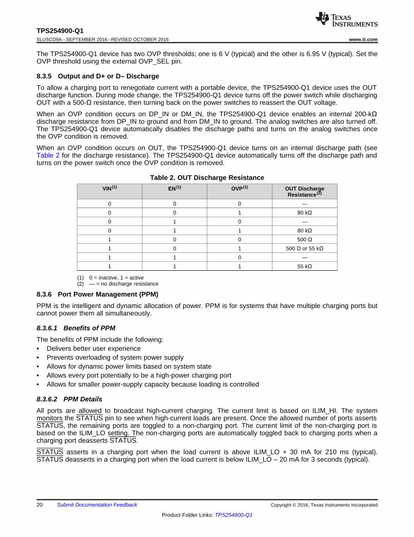
(1) 0 = inactive, 1 = active(2) — = no discharge resistance
Table 2. OUT Discharge ResistanceVIN (1) EN (1) OVP (1) OUT Discharge
Resistance (2)
0 0 0 —0 0 1 80 kΩ0 1 0 —0 1 1 80 kΩ1 0 0 500 Ω1 0 1 500 Ω or 55 kΩ1 1 0 —1 1 1 55 kΩ
8.3.6 Port Power Management (PPM)PPM is the intelligent and dynamic allocation of power. PPM is for systems that have multiple charging ports butcannot power them all simultaneously.
8.3.6.1 Benefits of PPMThe benefits of PPM include the following:• Delivers better user experience• Prevents overloading of system power supply• Allows for dynamic power limits based on system state• Allows every port potentially to be a high-power charging port• Allows for smaller power-supply capacity because loading is controlled
8.3.6.2 PPM DetailsAll ports are allowed to broadcast high-current charging. The current limit is based on ILIM_HI. The systemmonitors the STATUS pin to see when high-current loads are present. Once the allowed number of ports assertsSTATUS, the remaining ports are toggled to a non-charging port. The current limit of the non-charging port isbased on the ILIM_LO setting. The non-charging ports are automatically toggled back to charging ports when acharging port deasserts STATUS.
STATUS asserts in a charging port when the load current is above ILIM_LO + 30 mA for 210 ms (typical).STATUS deasserts in a charging port when the load current is below ILIM_LO – 20 mA for 3 seconds (typical).
IN OUT
DP_IN
DM_IN
ILIM_LO
ILIM_HI
GND
CTL1
CTL2
EN
TPS254900-Q1 Port 1
IN OUT
DP_IN
DM_IN
ILIM_LO
ILIM_HI
GND
CTL1
CTL2
EN
TPS254900-Q1 Port 2
100 kW
100 kW
EN1
FAULT1
EN2
USB Charging
Port 1
USB Charging
Port 2
RIL
IM_
HI
RIL
IM_
LO
5 V
FAULT
FAULT
FAULT2
STATUS
STATUS
RIL
IM_
HI
RIL
IM_
LO
Copyright © 2016, Texas Instruments Incorporated
21
TPS254900-Q1www.ti.com SLUSCO9A –SEPTEMBER 2016–REVISED OCTOBER 2016
Product Folder Links: TPS254900-Q1
Submit Documentation FeedbackCopyright © 2016, Texas Instruments Incorporated
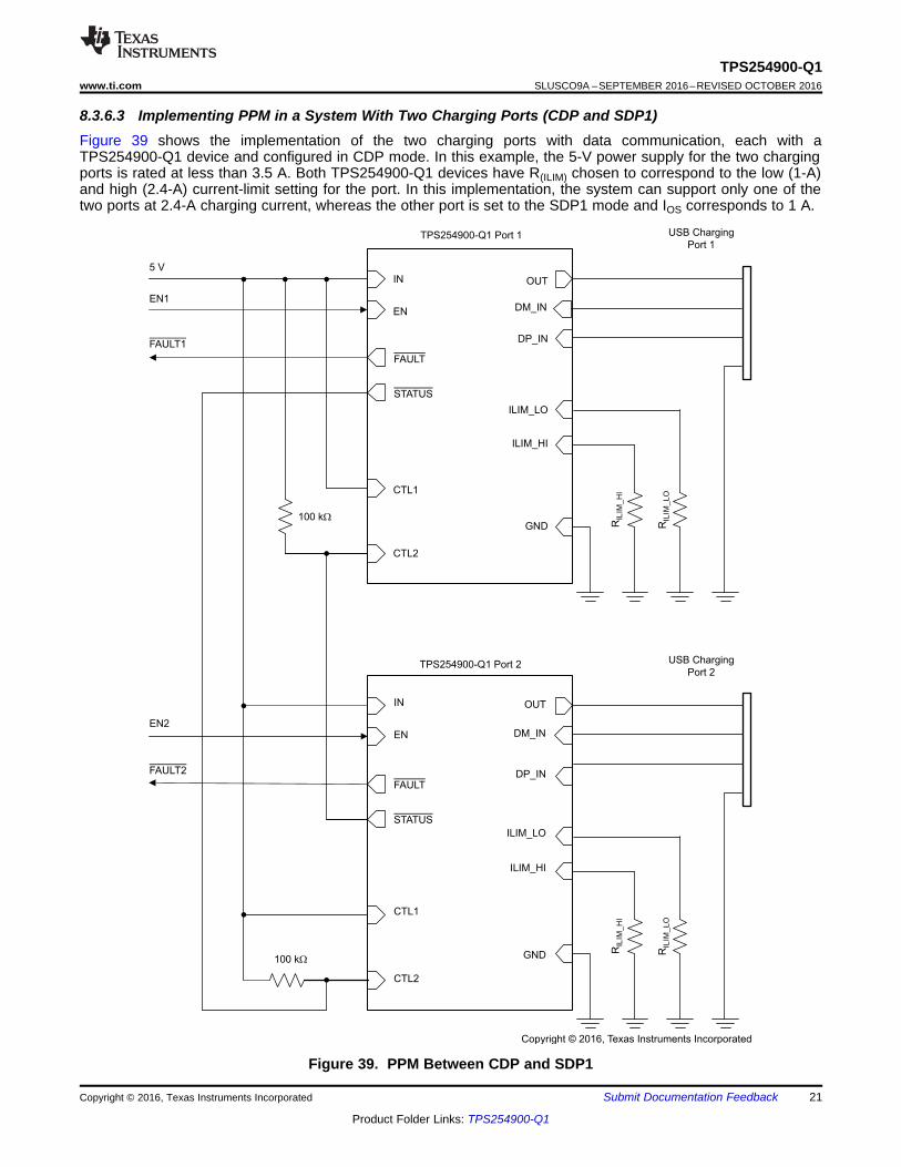
8.3.6.3 Implementing PPM in a System With Two Charging Ports (CDP and SDP1)Figure 39 shows the implementation of the two charging ports with data communication, each with aTPS254900-Q1 device and configured in CDP mode. In this example, the 5-V power supply for the two chargingports is rated at less than 3.5 A. Both TPS254900-Q1 devices have R(ILIM) chosen to correspond to the low (1-A)and high (2.4-A) current-limit setting for the port. In this implementation, the system can support only one of thetwo ports at 2.4-A charging current, whereas the other port is set to the SDP1 mode and IOS corresponds to 1 A.
Figure 39. PPM Between CDP and SDP1
OS(max) 0.9987(ILIM_ xx)
51 820 VI (mA) 38
R k= +
W
OS(min) 0.9974(ILIM_ xx)
46464 VI (mA) 32
R k= -
W
OS(nom) 0.9945(ILIM_ xx)
48687 VI (mA)
R k=
W
22
TPS254900-Q1SLUSCO9A –SEPTEMBER 2016–REVISED OCTOBER 2016 www.ti.com
Product Folder Links: TPS254900-Q1
Submit Documentation Feedback Copyright © 2016, Texas Instruments Incorporated
8.3.7 Overcurrent ProtectionWhen an overcurrent condition is detected, the device maintains a constant output current and reduces theoutput voltage accordingly. Two possible overload conditions can occur. In the first condition, the output isshorted before the device is enabled or before the application of V(IN). The TPS254900-Q1 device senses theshort and immediately switches into a constant-current output. In the second condition, a short or an overloadoccurs while the device is enabled. At the instant the overload occurs, high currents flow for 1 to 2 μs (typical)before the current-limit circuit reacts. The device operates in constant-current mode after the current-limit circuithas responded. Complete shutdown occurs only if the fault is present long enough to activate thermal limiting.The device remains off until the junction temperature cools approximately 20°C and then restarts. The devicecontinues to cycle on and off until the overcurrent condition is removed.
8.3.8 Undervoltage LockoutThe undervoltage-lockout (UVLO) circuit disables the power switch until the input voltage reaches the UVLOturnon threshold. Built-in hysteresis prevents unwanted oscillations on the output due to input voltage drop fromlarge current surges.
8.3.9 Thermal SensingTwo independent thermal-sensing circuits protect the TPS254900-Q1 device if the temperature exceedsrecommended operating conditions. These circuits monitor the operating temperature of the power-distributionswitch and disable operation. The power dissipation in the package is proportional to the voltage drop across thepower switch, so the junction temperature rises during an overcurrent condition. The first thermal sensor turns offthe power switch when the die temperature exceeds 135ºC and the device is in current limit. The second thermalsensor turns off the power switch when the die temperature exceeds 155ºC regardless of whether the powerswitch is in current limit. Hysteresis is built into both thermal sensors, and the switch turns on after the devicehas cooled by approximately 20°C. The switch continues to cycle off and then on until the fault is removed. Theopen-drain false-reporting output, FAULT, is asserted (low) during an overtemperature shutdown condition.
8.3.10 Current-Limit SettingThe TPS254900-Q1 has two independent current-limit settings that are each adjusted externally with a resistor.The ILIM_HI setting is adjusted with R(ILIM_HI) connected between ILIM_HI and GND. The ILIM_LO setting isadjusted with R(ILIM_LO) connected between ILIM_LO and GND. Consult the device truth table (Table 3) to seewhen each current limit is used. Both settings have the same relation between the current limit and the adjustingresistor.
The following equation calculates the value of resistor for adjusting the typical current limit:
(3)
Many applications require that the current limit meet specific tolerance limits. When designing to these tolerancelimits, both the tolerance of the TPS254900-Q1 current limit and the tolerance of the external adjusting resistormust be taken into account. The following equations approximate the TPS254900-Q1 minimum and maximumcurrent limits to within a few milliamperes and are appropriate for design purposes. The equations do notconstitute part of TI’s published device specifications for purposes of TI’s product warranty. These equationsassume an ideal—no variation—external adjusting resistor. To take resistor tolerance into account, firstdetermine the minimum and maximum resistor values based on its tolerance specifications and use these valuesin the equations. Because of the inverse relation between the current limit and the adjusting resistor, use themaximum resistor value in the IOS(min) equation and the minimum resistor value in the IOS(max) equation.
(4)
(5)
Adjusting Resistor (kW)
Curr
ent-
Lim
itT
hre
shold
(m
A)
10 20 30 40 50 60 70 80 90 1000
500
1000
1500
2000
2500
3000
3500
4000
D022
IOS, MinIOS, MaxIOS, Typ
Adjusting Resistor (kW)
Cu
rre
nt-
Lim
itT
hre
sho
ld(m
A)
100 200 300 400 500 600 700 800 900 10000
100
200
300
400
500
600
D023
IOS, MinIOS, MaxIOS, Typ
23
TPS254900-Q1www.ti.com SLUSCO9A –SEPTEMBER 2016–REVISED OCTOBER 2016
Product Folder Links: TPS254900-Q1
Submit Documentation FeedbackCopyright © 2016, Texas Instruments Incorporated
(1) No 5.1-kΩ resistor from BIAS to OUT (open between the pins), or OUT still has 5-V voltage from an external downstream port; clientmode is still active.
(2) No OUT discharge when changing from 10 to 11 or from 11 to 10.(3) A fault only trips OTSD, OUT, DP_IN, DM_IN, and OVP.
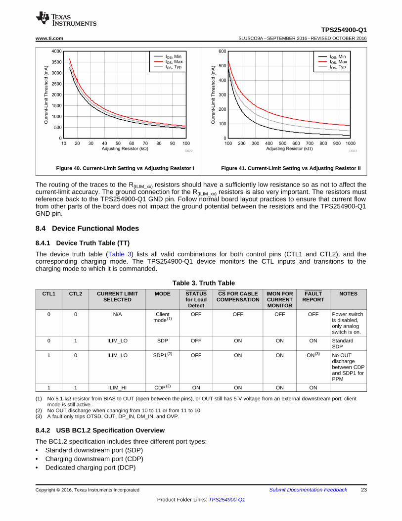
Figure 40. Current-Limit Setting vs Adjusting Resistor I Figure 41. Current-Limit Setting vs Adjusting Resistor II
The routing of the traces to the R(ILIM_xx) resistors should have a sufficiently low resistance so as not to affect thecurrent-limit accuracy. The ground connection for the R(ILIM_xx) resistors is also very important. The resistors mustreference back to the TPS254900-Q1 GND pin. Follow normal board layout practices to ensure that current flowfrom other parts of the board does not impact the ground potential between the resistors and the TPS254900-Q1GND pin.
8.4 Device Functional Modes
8.4.1 Device Truth Table (TT)The device truth table (Table 3) lists all valid combinations for both control pins (CTL1 and CTL2), and thecorresponding charging mode. The TPS254900-Q1 device monitors the CTL inputs and transitions to thecharging mode to which it is commanded.
Table 3. Truth TableCTL1 CTL2 CURRENT LIMIT
SELECTEDMODE STATUS
for LoadDetect
CS FOR CABLECOMPENSATION
IMON FORCURRENTMONITOR
FAULTREPORT
NOTES
0 0 N/A Clientmode (1)
OFF OFF OFF OFF Power switchis disabled,only analogswitch is on.
0 1 ILIM_LO SDP OFF ON ON ON StandardSDP
1 0 ILIM_LO SDP1 (2) OFF ON ON ON (3) No OUTdischargebetween CDPand SDP1 forPPM
1 1 ILIM_HI CDP (2) ON ON ON ON
8.4.2 USB BC1.2 Specification OverviewThe BC1.2 specification includes three different port types:• Standard downstream port (SDP)• Charging downstream port (CDP)• Dedicated charging port (DCP)
IN
OFF
DM_OUT
DP_OUT
DM_IN
DP_IN
OUT
Copyright © 2016, Texas Instruments Incorporated
24
TPS254900-Q1SLUSCO9A –SEPTEMBER 2016–REVISED OCTOBER 2016 www.ti.com
Product Folder Links: TPS254900-Q1
Submit Documentation Feedback Copyright © 2016, Texas Instruments Incorporated
BC1.2 defines a charging port as a downstream-facing USB port that provides power for charging portableequipment. Under this definition, CDP and DCP are defined as charging ports.
Table 4 lists the difference between these port types.
Table 4. Operating Modes TablePORT TYPE SUPPORTS USB2.0 COMMUNICATION MAXIMUM ALLOWABLE CURRENT
DRAWN BY PORTABLE EQUIPMENT (A)SDP (USB 2.0) YES 0.5SDP (USB 3.0) YES 0.9
CDP YES 1.5DCP NO 1.5
8.4.3 Standard Downstream Port (SDP) Mode — USB 2.0 and USB 3.0An SDP is a traditional USB port that follows the USB 2.0 or USB 3.0 protocol. An SDP supplies a minimum of500 mA per port for USB 2.0 and 900 mA per port for USB 3.0. USB 2.0 and USB 3.0 communication issupported, and the host controller must be active to allow charging.
8.4.4 Charging Downstream Port (CDP) ModeA CDP is a USB port that follows the USB BC1.2 specification and supplies a minimum of 1.5 A per port. A CDPprovides power and meets the USB 2.0 requirements for device enumeration. USB 2.0 communication issupported, and the host controller must be active to allow charging. The difference between CDP and SDP is thehost-charge handshaking logic that identifies this port as a CDP. A CDP is identifiable by a compliant BC1.2client device and allows for additional current draw by the client device.
The CDP handshaking process occurs in two steps. During the first step, the portable equipment outputs anominal 0.6-V output on the D+ line and reads the voltage input on the D– line. The portable device detects theconnection to an SDP if the voltage is less than the nominal data-detect voltage of 0.3 V. The portable devicedetects the connection to a CDP if the D– voltage is greater than the nominal data-detect voltage of 0.3 V andoptionally less than 0.8 V.
The second step is necessary for portable equipment to determine whether the equipment is connected to a CDPor a DCP. The portable device outputs a nominal 0.6-V output on the D– line and reads the voltage input on theD+ line. The portable device concludes the equipment is connected to a CDP if the data line being read remainsless than the nominal data detects voltage of 0.3 V. The portable device concludes it is connected to a DCP ifthe data line being read is greater than the nominal data-detect voltage of 0.3 V.
The TPS254900-Q1 integrates CDP detection protocol, used at a downstream port as the CDP controller tosupport CDP portable-device fast charge up to 1.5 A.
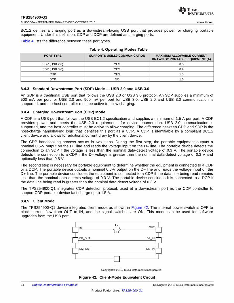
8.4.5 Client ModeThe TPS254900-Q1 device integrates client mode as shown in Figure 42. The internal power switch is OFF toblock current flow from OUT to IN, and the signal switches are ON. This mode can be used for softwareupgrades from the USB port.
Figure 42. Client-Mode Equivalent Circuit
25
TPS254900-Q1www.ti.com SLUSCO9A –SEPTEMBER 2016–REVISED OCTOBER 2016
Product Folder Links: TPS254900-Q1
Submit Documentation FeedbackCopyright © 2016, Texas Instruments Incorporated
Passing the IEC 61000-4-2 test for DP_IN and DM_IN requires connecting a discharge resistor to OUT duringUSB 2.0 high-speed enumeration. In client mode, because the power switch is OFF, OUT must be 5 V so thatthe device can work normally (usually powered by an external downstream USB port). If the OUT voltage is low,the communication may not work properly.
8.4.6 High-Bandwidth Data-Line SwitchThe D+ and D– data lines pass through the device to enable monitoring and handshaking while supporting thecharging operation. A wide-bandwidth signal switch allows data to pass through the device without corruptingsignal integrity. The data-line switches are turned on in any of the CDP, SDP or client operating modes. The ENinput must be at logic high for the data-line switches to be enabled.
NOTE• While in CDP mode, the data switches are ON, even during CDP handshaking.• The data switches are only for the USB-2.0 differential pair. In the case of a USB-3.0
host, the super-speed differential pairs must be routed directly to the USB connectorwithout passing through the TPS254900-Q1 device.
• Data switches are OFF during OUT (VBUS) discharge.
IN OUT
DP_IN
DM_IN
ILIM_LO
ILIM_HI
GND
CTL1
CTL2
CS
EN
TPS254900-Q1
5 V
EN
FAULT
FAULT
STATUSSTATUS
0.1
µF
US
BC
onnecto
r
Mode
Select I/O
VBUS
D+
D–
GND
ADC
Upstream DC-DC
Converter
DP_OUT
DM_OUT
IMON
OVP_SELLogic I/O
10
µF
BIAS
2.2 µF
0805
50 V
X7R
5.1
kΩ
SM
AJ18
10
0 k
Ω
10
0kΩ
10
0kΩ
2.5
5kΩ
19.1
kΩ
80
.6kΩ
10 µF
1210
35 V
X7R SM
AJ1
8
To Host
Controller
Copyright © 2016, Texas Instruments Incorporated
26
TPS254900-Q1SLUSCO9A –SEPTEMBER 2016–REVISED OCTOBER 2016 www.ti.com
Product Folder Links: TPS254900-Q1
Submit Documentation Feedback Copyright © 2016, Texas Instruments Incorporated
9 Application and Implementation
NOTEInformation in the following applications sections is not part of the TI componentspecification, and TI does not warrant its accuracy or completeness. TI’s customers areresponsible for determining suitability of components for their purposes. Customers shouldvalidate and test their design implementation to confirm system functionality.
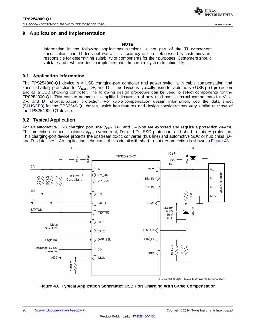
9.1 Application InformationThe TPS254900-Q1 device is a USB charging-port controller and power switch with cable compensation andshort-to-battery protection for VBUS, D+, and D–. The device is typically used for automotive USB port protectionand as a USB charging controller. The following design procedure can be used to select components for theTPS254900-Q1. This section presents a simplified discussion of how to choose external components for VBUS,D+, and D– short-to-battery protection. For cable-compensation design information, see the data sheet(SLUSCE3) for the TPS2549-Q1 device, which has features and design considerations very similar to those ofthe TPS254900-Q1 device.
9.2 Typical ApplicationFor an automotive USB charging port, the VBUS, D+, and D– pins are exposed and require a protection device.The protection required includes VBUS overcurrent, D+ and D– ESD protection, and short-to-battery protection.This charging-port device protects the upstream dc-dc converter (bus line) and automotive SOC or hub chips (D+and D– data lines). An application schematic of this circuit with short-to-battery protection is shown in Figure 43.
Figure 43. Typical Application Schematic: USB Port Charging With Cable Compensation
27
TPS254900-Q1www.ti.com SLUSCO9A –SEPTEMBER 2016–REVISED OCTOBER 2016
Product Folder Links: TPS254900-Q1
Submit Documentation FeedbackCopyright © 2016, Texas Instruments Incorporated
Typical Application (continued)9.2.1 Design RequirementsFor this design example, use the following as the input parameters.
DESIGN PARAMETER EXAMPLE VALUEBattery voltage, V(BAT) 18 VShort-circuit cable 0.5 m
9.2.2 Detailed Design ProcedureTo begin the design process, the designer must know the following:• The battery voltage• The short-circuit cable length• The maximum continuous output current for the charging port. The minimum current-limit setting of
TPS254900-Q1 device must be higher than this current.• The maximum output current of the upstream dc-dc converter. The maximum current-limit setting of
TPS254900-Q1 device must be lower than this current.• For cable compensation, the total resistance including power switch rDS(on), cable resistance, and connector
contact resistance must be specified.
9.2.2.1 Input CapacitanceConsider the following application situations when choosing the input capacitors.
For all applications, TI recommends a 0.1-µF or greater ceramic bypass capacitor between IN and GND, placedas close as possible to the device for local noise decoupling.
During output short or hot plug-in of a capacitive load, high current flows through the TPS254900-Q1 device backto the upstream dc-dc converter until the TPS254900-Q1 device responds (after t(IOS)). During this response time,the TPS254900-Q1 input capacitance and the dc-dc converter output capacitance source current to keep VINabove the UVLO of the TPS254900-Q1 device and any shared circuits. Size the input capacitance for theexpected transient conditions and keep the path between the TPS254900-Q1 device and the dc-dc convertershort to help minimize voltage drops.
Input voltage overshoots can be caused by either of two effects. The first cause is an abrupt application of inputvoltage in conjunction with input power-bus inductance and input capacitance when the IN pin is in the high-impedance state (before turnon). Theoretically, the peak voltage is 2 times the applied voltage. The secondcause is due to the abrupt reduction of output short-circuit current when the TPS254900-Q1 device turns off andenergy stored in the input inductance drives the input voltage high. Applications with large input inductance (forexample, a connection between the evaluation board and the bench power supply through long cables) mayrequire large input capacitance to prevent the voltage overshoot from exceeding the absolute-maximum voltageof the device.
During the short-to-battery (EN = HIGH) condition, the input voltage follows the output voltage until OVPprotection is triggered (t(OV_OUT)). After the TPS254900-Q1 device responds and turns off the power switch, thestored energy in the input inductance can cause ringing.
Based on the three situations described, 10-µF and 0.1-µF low-ESR ceramic capacitors, placed close to theinput, are recommended.
9.2.2.2 Output CapacitanceConsider the following application situations when choosing the output capacitors.
After an output short occurs, the TPS254900-Q1 device abruptly reduces the OUT current, and the energy storedin the output power-bus inductance causes voltage undershoot and potentially reverse voltage as it discharges.
Applications with large output inductance (such as from a cable) benefit from the use of a high-value outputcapacitor to control the voltage undershoot.
For USB port applications, because the VBUS pin is exposed to IEC61000-4-2 level-4 ESD, use a low-ESRcapacitance to protect OUT.
28
TPS254900-Q1SLUSCO9A –SEPTEMBER 2016–REVISED OCTOBER 2016 www.ti.com
Product Folder Links: TPS254900-Q1
Submit Documentation Feedback Copyright © 2016, Texas Instruments Incorporated
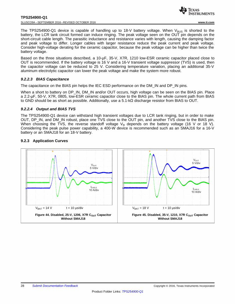
The TPS254900-Q1 device is capable of handling up to 18-V battery voltage. When VBUS is shorted to thebattery, the LCR tank circuit formed can induce ringing. The peak voltage seen on the OUT pin depends on theshort-circuit cable length. The parasitic inductance and resistance varies with length, causing the damping factorand peak voltage to differ. Longer cables with larger resistance reduce the peak current and peak voltage.Consider high-voltage derating for the ceramic capacitor, because the peak voltage can be higher than twice thebattery voltage.
Based on the three situations described, a 10-µF, 35-V, X7R, 1210 low-ESR ceramic capacitor placed close toOUT is recommended. If the battery voltage is 16 V and a 16-V transient voltage suppressor (TVS) is used, thenthe capacitor voltage can be reduced to 25 V. Considering temperature variation, placing an additional 35-Valuminum electrolytic capacitor can lower the peak voltage and make the system more robust.
9.2.2.3 BIAS CapacitanceThe capacitance on the BIAS pin helps the IEC ESD performance on the DM_IN and DP_IN pins.
When a short to battery on DP_IN, DM_IN and/or OUT occurs, high voltage can be seen on the BIAS pin. Placea 2.2-µF, 50-V, X7R, 0805, low-ESR ceramic capacitor close to the BIAS pin. The whole current path from BIASto GND should be as short as possible. Additionally, use a 5.1-kΩ discharge resistor from BIAS to OUT.
9.2.2.4 Output and BIAS TVSThe TPS254900-Q1 device can withstand high transient voltages due to LCR tank ringing, but in order to makeOUT, DP_IN, and DM_IN robust, place one TVS close to the OUT pin, and another TVS close to the BIAS pin.When choosing the TVS, the reverse standoff voltage VR depends on the battery voltage (16 V or 18 V).Considering the peak pulse power capability, a 400-W device is recommended such as an SMAJ16 for a 16-Vbattery or an SMAJ18 for an 18-V battery.
9.2.3 Application Curves
VBAT = 14 V t = 10 µs/div
Figure 44. Disabled, 25-V, 1206, X7R COUT CapacitorWithout SMAJ18
VBAT = 18 V t = 10 µs/div
Figure 45. Disabled, 35-V, 1210, X7R COUT CapacitorWithout SMAJ18
29
TPS254900-Q1www.ti.com SLUSCO9A –SEPTEMBER 2016–REVISED OCTOBER 2016
Product Folder Links: TPS254900-Q1
Submit Documentation FeedbackCopyright © 2016, Texas Instruments Incorporated
t = 10 µs/div
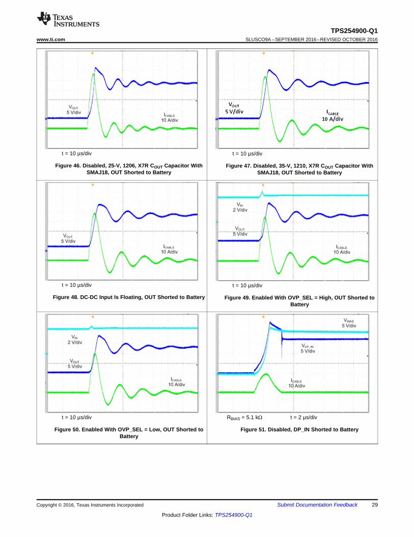
Figure 46. Disabled, 25-V, 1206, X7R COUT Capacitor WithSMAJ18, OUT Shorted to Battery
t = 10 µs/div
Figure 47. Disabled, 35-V, 1210, X7R COUT Capacitor WithSMAJ18, OUT Shorted to Battery
t = 10 µs/div
Figure 48. DC-DC Input Is Floating, OUT Shorted to Battery
t = 10 µs/div
Figure 49. Enabled With OVP_SEL = High, OUT Shorted toBattery
t = 10 µs/div
Figure 50. Enabled With OVP_SEL = Low, OUT Shorted toBattery
RBIAS = 5.1 kΩ t = 2 µs/div
Figure 51. Disabled, DP_IN Shorted to Battery
30
TPS254900-Q1SLUSCO9A –SEPTEMBER 2016–REVISED OCTOBER 2016 www.ti.com
Product Folder Links: TPS254900-Q1
Submit Documentation Feedback Copyright © 2016, Texas Instruments Incorporated
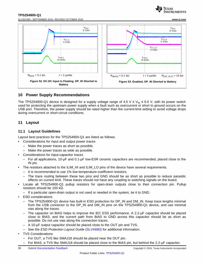
RBIAS = 5.1 kΩ t = 2 µs/div
Figure 52. DC-DC Input Is Floating, DP_IN Shorted toBattery
R(BIAS) = 5.1 kΩ t = 2 µs/div R(DP_OUT) = 15 kΩ
Figure 53. Enabled, DP_IN Shorted to Battery
10 Power Supply RecommendationsThe TPS254900-Q1 device is designed for a supply voltage range of 4.5 V ≤ VIN ≤ 6.5 V, with its power switchused for protecting the upstream power supply when a fault such as overcurrent or short to ground occurs on theUSB port. Therefore, the power supply should be rated higher than the current-limit setting to avoid voltage dropsduring overcurrent or short-circuit conditions.
11 Layout
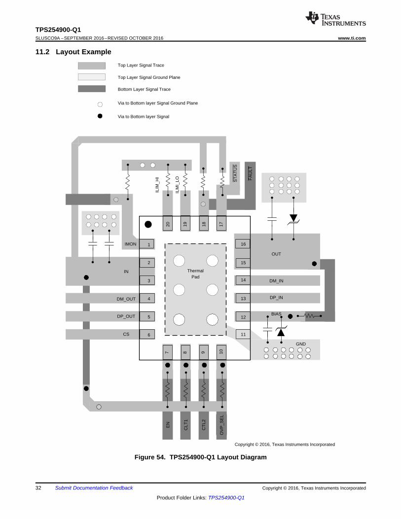
11.1 Layout GuidelinesLayout best practices for the TPS254900-Q1 are listed as follows.• Considerations for input and output power traces
– Make the power traces as short as possible.– Make the power traces as wide as possible.
• Considerations for input-capacitor traces– For all applications, 10-µF and 0.1-µF low-ESR ceramic capacitors are recommended, placed close to the
IN pin.• The resistors attached to the ILIM_HI and ILIM_LO pins of the device have several requirements.
– It is recommended to use 1% low-temperature-coefficient resistors.– The trace routing between these two pins and GND should be as short as possible to reduce parasitic
effects on current limit. These traces should not have any coupling to switching signals on the board.• Locate all TPS254900-Q1 pullup resistors for open-drain outputs close to their connection pin. Pullup
resistors should be 100 kΩ.– If a particular open-drain output is not used or needed in the system, tie it to GND.
• ESD considerations– The TPS254900-Q1 device has built-in ESD protection for DP_IN and DM_IN. Keep trace lengths minimal
from the USB connector to the DP_IN and DM_IN pins on the TPS254900-Q1 device, and use minimalvias along the traces.
– The capacitor on BIAS helps to improve the IEC ESD performance. A 2.2-µF capacitor should be placedclose to BIAS, and the current path from BIAS to GND across this capacitor should be as short aspossible. Do not use vias along the connection traces.
– A 10-µF output capacitor should be placed close to the OUT pin and TVS.– See the ESD Protection Layout Guide (SLVA680) for additional information.
• TVS Considerations– For OUT, a TVS like SMAJ18 should be placed near the OUT pin.– For BIAS, a TVS like SMAJ18 should be placed close to the BIAS pin, but behind the 2.2-µF capacitor.
31
TPS254900-Q1www.ti.com SLUSCO9A –SEPTEMBER 2016–REVISED OCTOBER 2016
Product Folder Links: TPS254900-Q1
Submit Documentation FeedbackCopyright © 2016, Texas Instruments Incorporated
Layout Guidelines (continued)– The whole path from OUT to GND or BIAS to GND across the TVS should be as short as possible.
• DP_IN, DM_IN, DP_OUT, and DM_OUT routing considerations– Route these traces as microstrips with nominal differential impedance of 90 Ω.– Minimize the use of vias on the high-speed data lines.– Keep the reference GND plane devoid from cuts or splits above the differential pairs to prevent impedance
discontinuities.– For more USB 2.0 high-speed D+ and D– differential routing information, see the High Speed USB
Platform Design Guideline from Intel.• Thermal Considerations
– When properly mounted, the thermal-pad package provides significantly greater cooling ability than anordinary package. To operate at rated power, the thermal pad must be soldered to the board GND planedirectly under the device. The thermal pad is at GND potential and can be connected using multiple viasto inner-layer GND. Other planes, such as the bottom side of the circuit board, can be used to increaseheat sinking in higher-current applications. See the PowerPad™ Thermally Enhanced Package applicationreport (SLMA002) and PowerPAD™ Made Easy application brief (SLMA004) for more information onusing this thermal pad package.
1
2
3
4
7 8 9 1017181920
IMON
IN
OUT
DM_OUT
DM_IN
DP_IN
Via to Bottom layer Signal Ground Plane
Via to Bottom layer Signal
Top Layer Signal Trace
Top Layer Signal Ground Plane
Bottom Layer Signal Trace
xx
xx
xxxxxxxx
x
xxxx
Thermal Pad
5
6CS
BIAS
GND
xx
xx
xx
xx
xxx
ST
AT
US
FA
ULT
OV
P_S
EL
CT
L2
CLT
1
EN
16
15
14
13
12
11
ILIM
_HI
ILM
I_LO
DP_OUT
Copyright © 2016, Texas Instruments Incorporated
32
TPS254900-Q1SLUSCO9A –SEPTEMBER 2016–REVISED OCTOBER 2016 www.ti.com
Product Folder Links: TPS254900-Q1
Submit Documentation Feedback Copyright © 2016, Texas Instruments Incorporated
11.2 Layout Example
Figure 54. TPS254900-Q1 Layout Diagram
33
TPS254900-Q1www.ti.com SLUSCO9A –SEPTEMBER 2016–REVISED OCTOBER 2016
Product Folder Links: TPS254900-Q1
Submit Documentation FeedbackCopyright © 2016, Texas Instruments Incorporated
12 Device and Documentation Support
12.1 Device Support
12.1.1 Third-Party Products DisclaimerTI'S PUBLICATION OF INFORMATION REGARDING THIRD-PARTY PRODUCTS OR SERVICES DOES NOTCONSTITUTE AN ENDORSEMENT REGARDING THE SUITABILITY OF SUCH PRODUCTS OR SERVICESOR A WARRANTY, REPRESENTATION OR ENDORSEMENT OF SUCH PRODUCTS OR SERVICES, EITHERALONE OR IN COMBINATION WITH ANY TI PRODUCT OR SERVICE.
12.2 Documentation Support
12.2.1 Related DocumentationHigh Speed USB Platform Design Guidelines, Intel
12.3 Receiving Notification of Documentation UpdatesTo receive notification of documentation updates, navigate to the device product folder on ti.com. In the upperright corner, click on Alert me to register and receive a weekly digest of any product information that haschanged. For change details, review the revision history included in any revised document.
12.4 Community ResourcesThe following links connect to TI community resources. Linked contents are provided "AS IS" by the respectivecontributors. They do not constitute TI specifications and do not necessarily reflect TI's views; see TI's Terms ofUse.
TI E2E™ Online Community TI's Engineer-to-Engineer (E2E) Community. Created to foster collaborationamong engineers. At e2e.ti.com, you can ask questions, share knowledge, explore ideas and helpsolve problems with fellow engineers.
Design Support TI's Design Support Quickly find helpful E2E forums along with design support tools andcontact information for technical support.
12.5 TrademarksE2E is a trademark of Texas Instruments.All other trademarks are the property of their respective owners.
12.6 Electrostatic Discharge CautionThese devices have limited built-in ESD protection. The leads should be shorted together or the device placed in conductive foamduring storage or handling to prevent electrostatic damage to the MOS gates.
12.7 GlossarySLYZ022 — TI Glossary.
This glossary lists and explains terms, acronyms, and definitions.
13 Mechanical, Packaging, and Orderable InformationThe following pages include mechanical, packaging, and orderable information. This information is the most-current data available for the designated device. This data is subject to change without notice and withoutrevision of this document. For browser-based versions of this data sheet, see the left-hand navigation pane.
PACKAGE OPTION ADDENDUM
www.ti.com 23-Nov-2016
Addendum-Page 1
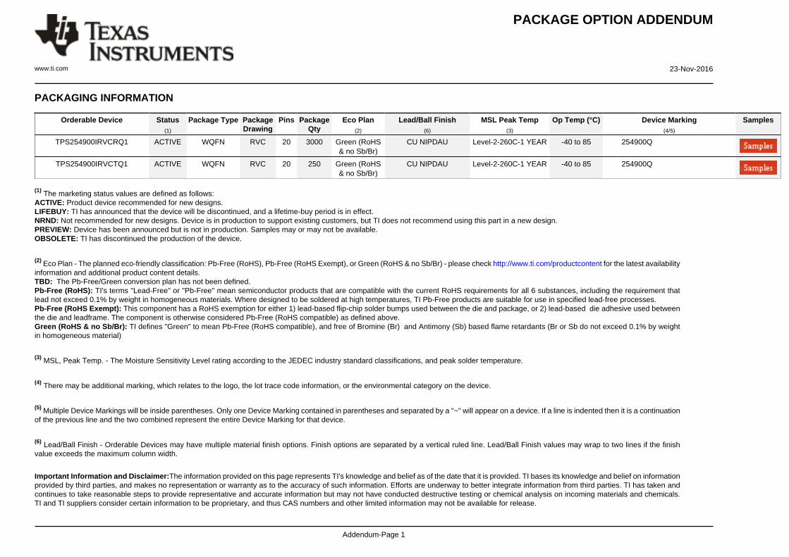
PACKAGING INFORMATION
Orderable Device Status(1)
Package Type PackageDrawing
Pins PackageQty
Eco Plan(2)
Lead/Ball Finish(6)
MSL Peak Temp(3)
Op Temp (°C) Device Marking(4/5)
Samples
TPS254900IRVCRQ1 ACTIVE WQFN RVC 20 3000 Green (RoHS& no Sb/Br)
CU NIPDAU Level-2-260C-1 YEAR -40 to 85 254900Q
TPS254900IRVCTQ1 ACTIVE WQFN RVC 20 250 Green (RoHS& no Sb/Br)
CU NIPDAU Level-2-260C-1 YEAR -40 to 85 254900Q
(1) The marketing status values are defined as follows:ACTIVE: Product device recommended for new designs.LIFEBUY: TI has announced that the device will be discontinued, and a lifetime-buy period is in effect.NRND: Not recommended for new designs. Device is in production to support existing customers, but TI does not recommend using this part in a new design.PREVIEW: Device has been announced but is not in production. Samples may or may not be available.OBSOLETE: TI has discontinued the production of the device.
(2) Eco Plan - The planned eco-friendly classification: Pb-Free (RoHS), Pb-Free (RoHS Exempt), or Green (RoHS & no Sb/Br) - please check http://www.ti.com/productcontent for the latest availabilityinformation and additional product content details.TBD: The Pb-Free/Green conversion plan has not been defined.Pb-Free (RoHS): TI's terms "Lead-Free" or "Pb-Free" mean semiconductor products that are compatible with the current RoHS requirements for all 6 substances, including the requirement thatlead not exceed 0.1% by weight in homogeneous materials. Where designed to be soldered at high temperatures, TI Pb-Free products are suitable for use in specified lead-free processes.Pb-Free (RoHS Exempt): This component has a RoHS exemption for either 1) lead-based flip-chip solder bumps used between the die and package, or 2) lead-based die adhesive used betweenthe die and leadframe. The component is otherwise considered Pb-Free (RoHS compatible) as defined above.Green (RoHS & no Sb/Br): TI defines "Green" to mean Pb-Free (RoHS compatible), and free of Bromine (Br) and Antimony (Sb) based flame retardants (Br or Sb do not exceed 0.1% by weightin homogeneous material)
(3) MSL, Peak Temp. - The Moisture Sensitivity Level rating according to the JEDEC industry standard classifications, and peak solder temperature.
(4) There may be additional marking, which relates to the logo, the lot trace code information, or the environmental category on the device.
(5) Multiple Device Markings will be inside parentheses. Only one Device Marking contained in parentheses and separated by a "~" will appear on a device. If a line is indented then it is a continuationof the previous line and the two combined represent the entire Device Marking for that device.
(6) Lead/Ball Finish - Orderable Devices may have multiple material finish options. Finish options are separated by a vertical ruled line. Lead/Ball Finish values may wrap to two lines if the finishvalue exceeds the maximum column width.
Important Information and Disclaimer:The information provided on this page represents TI's knowledge and belief as of the date that it is provided. TI bases its knowledge and belief on informationprovided by third parties, and makes no representation or warranty as to the accuracy of such information. Efforts are underway to better integrate information from third parties. TI has taken andcontinues to take reasonable steps to provide representative and accurate information but may not have conducted destructive testing or chemical analysis on incoming materials and chemicals.TI and TI suppliers consider certain information to be proprietary, and thus CAS numbers and other limited information may not be available for release.
PACKAGE OPTION ADDENDUM
www.ti.com 23-Nov-2016
Addendum-Page 2
In no event shall TI's liability arising out of such information exceed the total purchase price of the TI part(s) at issue in this document sold by TI to Customer on an annual basis.
TAPE AND REEL INFORMATION
*All dimensions are nominal
Device PackageType
PackageDrawing
Pins SPQ ReelDiameter
(mm)
ReelWidth
W1 (mm)
A0(mm)
B0(mm)
K0(mm)
P1(mm)
W(mm)
Pin1Quadrant
TPS254900IRVCRQ1 WQFN RVC 20 3000 330.0 12.4 3.3 4.3 1.1 8.0 12.0 Q1
TPS254900IRVCTQ1 WQFN RVC 20 250 180.0 12.4 3.3 4.3 1.1 8.0 12.0 Q1
PACKAGE MATERIALS INFORMATION
www.ti.com 24-Nov-2016
Pack Materials-Page 1
*All dimensions are nominal
Device Package Type Package Drawing Pins SPQ Length (mm) Width (mm) Height (mm)
TPS254900IRVCRQ1 WQFN RVC 20 3000 367.0 367.0 35.0
TPS254900IRVCTQ1 WQFN RVC 20 250 210.0 185.0 35.0
PACKAGE MATERIALS INFORMATION
www.ti.com 24-Nov-2016
Pack Materials-Page 2
www.ti.com
PACKAGE OUTLINE
C
SEE TERMINALDETAIL
20X 0.250.15
1.6 0.1
20X 0.450.35
0.8 MAX
(0.2) TYP
0.050.00
16X 0.5
2X2.5
2X 1.5
2.6 0.1
B 3.12.9
A
4.13.9
0.250.15
0.450.35
WQFN - 0.8 mm max heightRVC0020APLASTIC QUAD FLATPACK - NO LEAD
4219150/B 03/2017
PIN 1 INDEX AREA
0.08
SEATING PLANE
1
6 11
16
7 10
20 17(OPTIONAL)
PIN 1 ID 0.1 C A B0.05
EXPOSEDTHERMAL PAD
21 SYMM
SYMM
NOTES: 1. All linear dimensions are in millimeters. Any dimensions in parenthesis are for reference only. Dimensioning and tolerancing per ASME Y14.5M. 2. This drawing is subject to change without notice. 3. The package thermal pad must be soldered to the printed circuit board for optimal thermal and mechanical performance.
SCALE 3.700
DETAILOPTIONAL TERMINAL
TYPICAL
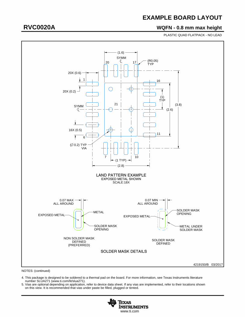
www.ti.com
EXAMPLE BOARD LAYOUT
0.07 MINALL AROUND
0.07 MAXALL AROUND
20X (0.2)
20X (0.6)
( 0.2) TYPVIA
16X (0.5)
(3.8)
(2.8)
(1)TYP
(1.6)
(R0.05)TYP
(2.6)
(1 TYP)
WQFN - 0.8 mm max heightRVC0020APLASTIC QUAD FLATPACK - NO LEAD
4219150/B 03/2017
SYMM
1
6
7 10
11
16
1720
SYMM
LAND PATTERN EXAMPLEEXPOSED METAL SHOWN
SCALE:18X
21
NOTES: (continued) 4. This package is designed to be soldered to a thermal pad on the board. For more information, see Texas Instruments literature number SLUA271 (www.ti.com/lit/slua271).5. Vias are optional depending on application, refer to device data sheet. If any vias are implemented, refer to their locations shown on this view. It is recommended that vias under paste be filled, plugged or tented.
SOLDER MASKOPENING
METAL UNDERSOLDER MASK
SOLDER MASKDEFINED
EXPOSED METALMETAL
SOLDER MASKOPENING
SOLDER MASK DETAILS
NON SOLDER MASKDEFINED
(PREFERRED)
EXPOSED METAL
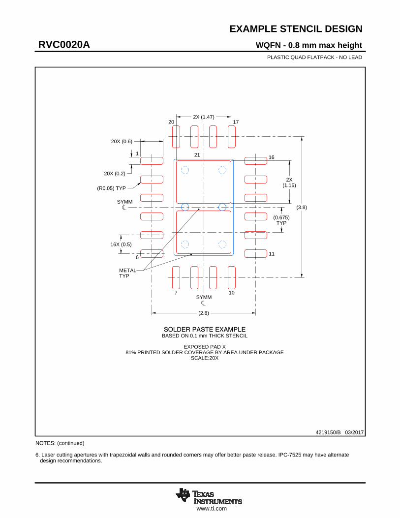
www.ti.com
EXAMPLE STENCIL DESIGN
20X (0.6)
20X (0.2)
16X (0.5)
(2.8)
(3.8)
2X (1.47)
(0.675)TYP
(R0.05) TYP2X
(1.15)
WQFN - 0.8 mm max heightRVC0020APLASTIC QUAD FLATPACK - NO LEAD
4219150/B 03/2017
NOTES: (continued) 6. Laser cutting apertures with trapezoidal walls and rounded corners may offer better paste release. IPC-7525 may have alternate design recommendations.
SYMM
METALTYP
SOLDER PASTE EXAMPLEBASED ON 0.1 mm THICK STENCIL
EXPOSED PAD X
81% PRINTED SOLDER COVERAGE BY AREA UNDER PACKAGESCALE:20X
SYMM
1
6
7 10
11
16
1720
21
IMPORTANT NOTICE
Texas Instruments Incorporated (TI) reserves the right to make corrections, enhancements, improvements and other changes to itssemiconductor products and services per JESD46, latest issue, and to discontinue any product or service per JESD48, latest issue. Buyersshould obtain the latest relevant information before placing orders and should verify that such information is current and complete.TI’s published terms of sale for semiconductor products (http://www.ti.com/sc/docs/stdterms.htm) apply to the sale of packaged integratedcircuit products that TI has qualified and released to market. Additional terms may apply to the use or sale of other types of TI products andservices.Reproduction of significant portions of TI information in TI data sheets is permissible only if reproduction is without alteration and isaccompanied by all associated warranties, conditions, limitations, and notices. TI is not responsible or liable for such reproduceddocumentation. Information of third parties may be subject to additional restrictions. Resale of TI products or services with statementsdifferent from or beyond the parameters stated by TI for that product or service voids all express and any implied warranties for theassociated TI product or service and is an unfair and deceptive business practice. TI is not responsible or liable for any such statements.Buyers and others who are developing systems that incorporate TI products (collectively, “Designers”) understand and agree that Designersremain responsible for using their independent analysis, evaluation and judgment in designing their applications and that Designers havefull and exclusive responsibility to assure the safety of Designers' applications and compliance of their applications (and of all TI productsused in or for Designers’ applications) with all applicable regulations, laws and other applicable requirements. Designer represents that, withrespect to their applications, Designer has all the necessary expertise to create and implement safeguards that (1) anticipate dangerousconsequences of failures, (2) monitor failures and their consequences, and (3) lessen the likelihood of failures that might cause harm andtake appropriate actions. Designer agrees that prior to using or distributing any applications that include TI products, Designer willthoroughly test such applications and the functionality of such TI products as used in such applications.TI’s provision of technical, application or other design advice, quality characterization, reliability data or other services or information,including, but not limited to, reference designs and materials relating to evaluation modules, (collectively, “TI Resources”) are intended toassist designers who are developing applications that incorporate TI products; by downloading, accessing or using TI Resources in anyway, Designer (individually or, if Designer is acting on behalf of a company, Designer’s company) agrees to use any particular TI Resourcesolely for this purpose and subject to the terms of this Notice.TI’s provision of TI Resources does not expand or otherwise alter TI’s applicable published warranties or warranty disclaimers for TIproducts, and no additional obligations or liabilities arise from TI providing such TI Resources. TI reserves the right to make corrections,enhancements, improvements and other changes to its TI Resources. TI has not conducted any testing other than that specificallydescribed in the published documentation for a particular TI Resource.Designer is authorized to use, copy and modify any individual TI Resource only in connection with the development of applications thatinclude the TI product(s) identified in such TI Resource. NO OTHER LICENSE, EXPRESS OR IMPLIED, BY ESTOPPEL OR OTHERWISETO ANY OTHER TI INTELLECTUAL PROPERTY RIGHT, AND NO LICENSE TO ANY TECHNOLOGY OR INTELLECTUAL PROPERTYRIGHT OF TI OR ANY THIRD PARTY IS GRANTED HEREIN, including but not limited to any patent right, copyright, mask work right, orother intellectual property right relating to any combination, machine, or process in which TI products or services are used. Informationregarding or referencing third-party products or services does not constitute a license to use such products or services, or a warranty orendorsement thereof. Use of TI Resources may require a license from a third party under the patents or other intellectual property of thethird party, or a license from TI under the patents or other intellectual property of TI.TI RESOURCES ARE PROVIDED “AS IS” AND WITH ALL FAULTS. TI DISCLAIMS ALL OTHER WARRANTIES ORREPRESENTATIONS, EXPRESS OR IMPLIED, REGARDING RESOURCES OR USE THEREOF, INCLUDING BUT NOT LIMITED TOACCURACY OR COMPLETENESS, TITLE, ANY EPIDEMIC FAILURE WARRANTY AND ANY IMPLIED WARRANTIES OFMERCHANTABILITY, FITNESS FOR A PARTICULAR PURPOSE, AND NON-INFRINGEMENT OF ANY THIRD PARTY INTELLECTUALPROPERTY RIGHTS. TI SHALL NOT BE LIABLE FOR AND SHALL NOT DEFEND OR INDEMNIFY DESIGNER AGAINST ANY CLAIM,INCLUDING BUT NOT LIMITED TO ANY INFRINGEMENT CLAIM THAT RELATES TO OR IS BASED ON ANY COMBINATION OFPRODUCTS EVEN IF DESCRIBED IN TI RESOURCES OR OTHERWISE. IN NO EVENT SHALL TI BE LIABLE FOR ANY ACTUAL,DIRECT, SPECIAL, COLLATERAL, INDIRECT, PUNITIVE, INCIDENTAL, CONSEQUENTIAL OR EXEMPLARY DAMAGES INCONNECTION WITH OR ARISING OUT OF TI RESOURCES OR USE THEREOF, AND REGARDLESS OF WHETHER TI HAS BEENADVISED OF THE POSSIBILITY OF SUCH DAMAGES.Unless TI has explicitly designated an individual product as meeting the requirements of a particular industry standard (e.g., ISO/TS 16949and ISO 26262), TI is not responsible for any failure to meet such industry standard requirements.Where TI specifically promotes products as facilitating functional safety or as compliant with industry functional safety standards, suchproducts are intended to help enable customers to design and create their own applications that meet applicable functional safety standardsand requirements. Using products in an application does not by itself establish any safety features in the application. Designers mustensure compliance with safety-related requirements and standards applicable to their applications. Designer may not use any TI products inlife-critical medical equipment unless authorized officers of the parties have executed a special contract specifically governing such use.Life-critical medical equipment is medical equipment where failure of such equipment would cause serious bodily injury or death (e.g., lifesupport, pacemakers, defibrillators, heart pumps, neurostimulators, and implantables). Such equipment includes, without limitation, allmedical devices identified by the U.S. Food and Drug Administration as Class III devices and equivalent classifications outside the U.S.TI may expressly designate certain products as completing a particular qualification (e.g., Q100, Military Grade, or Enhanced Product).Designers agree that it has the necessary expertise to select the product with the appropriate qualification designation for their applicationsand that proper product selection is at Designers’ own risk. Designers are solely responsible for compliance with all legal and regulatoryrequirements in connection with such selection.Designer will fully indemnify TI and its representatives against any damages, costs, losses, and/or liabilities arising out of Designer’s non-compliance with the terms and provisions of this Notice.
Mailing Address: Texas Instruments, Post Office Box 655303, Dallas, Texas 75265Copyright © 2018, Texas Instruments Incorporated