TP2301 TP2302 8-Pin SOIC TP2301/TP2302 /TP2304 8-Pin …
16
3PEAK 1 TP2301/TP2302 /TP2304 20MHz Bandwidth, Low Noise High Precision Op-amps www.3peakic.com.cn Rev. A.2 Features Gain-bandwidth Product: 20MHz Offset Voltage: 50 μV (max) Low Noise: 7.3nV/√Hz(f= 1kHz) Slew Rate: 25 V/μs Low THD+N: 0.0005% Supply Range: 2.2V to 5.5V Supply Current: 3.5 mA/ch Low Input Bias Current: 0.3pA Typical Rail-to-Rail I/O High Output Current: 70mA (1.0V Drop) –40°C to 125°C Operation Range Applications Sensor Signal Conditioning Consumer Audio Multi-Pole Active Filters Control-Loop Amplifiers Communications Security Scanners Pin Configuration (Top View) TP2302 8-Pin SOIC/MSOP (-S and -V Suffixes) 8 6 5 7 3 2 1 4 Out A ﹢In A ﹣In A ﹢In B ﹣In B Out B A B ﹣Vs ﹢Vs TP2304 14-Pin SOIC/TSSOP (-S and -T Suffixes) 14 13 12 11 10 9 8 6 5 7 3 2 1 4 Out A ﹢In A ﹣In A D A C B Out D ﹢In D ﹣In D Out B ﹢In B ﹣In B Out C ﹢In C ﹣In C ﹣Vs ﹢Vs TP2301 8-Pin SOIC (-S Suffix) Out TP2301 5-Pin SOT23 (-T Suffix) 8 6 5 7 3 2 1 4 NC ﹢In ﹣In ﹣Vs ﹢Vs NC NC 4 5 3 2 1 Out +In -In ﹣Vs ﹢Vs Description The TP2301 series products are very high precision amplifiers featuring very low noise, low offset voltage, high bandwidth, low input bias current and low temperature drift making them the ideal choice for applications requiring both high DC accuracy and AC performance. The combination of precision, low noise, and high bandwidth provides the user with outstanding value and flexibility relative to similar competitive parts. Applications for these amplifiers include precision active filters, medical and analytical instrumentation, precision power supply controls, and industrial controls requiring high gains. Featuring low THD+N, the TP2301 series is also excellent for consumer audio applications, particularly for single-supply systems. The TP2301 is single channel version available in 8-pin SOIC and 5-pin SOT23 packages. The TP2302 is dual channel version available in 8-pin SOIC and MSOP packages. The TP2304 is quad channel version available in 14-pin SOIC and TSSOP packages. 3PEAK and the 3PEAK logo are registered trademarks of 3PEAK INCORPORATED. All other trademarks are the property of their respective owners. Positive Output Swing vs. Load Current 0 1 2 3 4 5 6 0 0.05 0.1 0.15 0.2 Vdrop(V) I source(A) T=-40℃ T=25℃ T=130℃
Transcript of TP2301 TP2302 8-Pin SOIC TP2301/TP2302 /TP2304 8-Pin …
3PEAK
1
TP2301/TP2302 /TP2304
20MHz Bandwidth, Low Noise High Precision Op-amps
www.3peakic.com.cn Rev. A.2
Features
Gain-bandwidth Product: 20MHz
Offset Voltage: 50 μV (max)
Low Noise: 7.3nV/√Hz(f= 1kHz)
Slew Rate: 25 V/μs
Low THD+N: 0.0005%
Supply Range: 2.2V to 5.5V
Supply Current: 3.5 mA/ch
Low Input Bias Current: 0.3pA Typical
Rail-to-Rail I/O
High Output Current: 70mA (1.0V Drop)
–40°C to 125°C Operation Range
Applications
Sensor Signal Conditioning
Consumer Audio
Multi-Pole Active Filters
Control-Loop Amplifiers
Communications
Security
Scanners
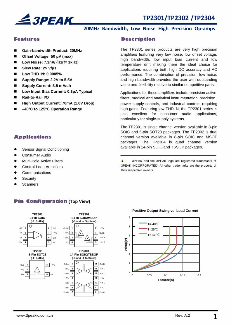
Pin Configuration (Top View)
TP2302
8-Pin SOIC/MSOP(-S and -V Suffixes)
8
6
5
7
3
2
1
4
Out A
﹢In A
﹣In A
﹢In B
﹣In B
Out BA
B
﹣Vs
﹢Vs
TP2304
14-Pin SOIC/TSSOP(-S and -T Suffixes)
14
13
12
11
10
9
8
6
5
7
3
2
1
4
Out A
﹢In A
﹣In ADA
CB
Out D
﹢In D
﹣In D
Out B
﹢In B
﹣In B
Out C
﹢In C
﹣In C
﹣Vs﹢Vs
TP2301
8-Pin SOIC(-S Suffix)
Out
TP2301
5-Pin SOT23(-T Suffix)
8
6
5
7
3
2
1
4
NC
﹢In
﹣In
﹣Vs
﹢Vs
NC
NC
4
5
3
2
1Out
+In -In
﹣Vs
﹢Vs
Description
The TP2301 series products are very high precision
amplifiers featuring very low noise, low offset voltage,
high bandwidth, low input bias current and low
temperature drift making them the ideal choice for
applications requiring both high DC accuracy and AC
performance. The combination of precision, low noise,
and high bandwidth provides the user with outstanding
value and flexibility relative to similar competitive parts.
Applications for these amplifiers include precision active
filters, medical and analytical instrumentation, precision
power supply controls, and industrial controls requiring
high gains. Featuring low THD+N, the TP2301 series is
also excellent for consumer audio applications,
particularly for single-supply systems.
The TP2301 is single channel version available in 8-pin
SOIC and 5-pin SOT23 packages. The TP2302 is dual
channel version available in 8-pin SOIC and MSOP
packages. The TP2304 is quad channel version
available in 14-pin SOIC and TSSOP packages.
3PEAK and the 3PEAK logo are registered trademarks of
3PEAK INCORPORATED. All other trademarks are the property of
their respective owners.
Positive Output Swing vs. Load Current
0
1
2
3
4
5
6
0 0.05 0.1 0.15 0.2
Vd
rop
(V)
I source(A)
T=-40℃
T=25℃
T=130℃
2 Rev.A.2
www.3peakic.com.cn
TP2301 / TP2302 / TP2304
20MHz Bandwidth, Low Noise High Precision Op-amps
Order Information
Model Name Order Number Package Transport Media, Quantity Marking
Information
TP2301 TP2301-SR 8-Pin SOIC Tape and Reel, 4,000 TP2301
TP2301-TR 5-Pin SOT23 Tape and Reel, 3,000 301
TP2302 TP2302-SR 8-Pin SOIC Tape and Reel, 4,000 TP2302
TP2302-VR 8-Pin MSOP Tape and Reel, 3,000 TP2302
TP2304 TP2304-SR 14-Pin SOIC Tape and Reel, 2,500 TP2304
TP2304-TR 14-Pin TSSOP Tape and Reel, 3,000 TP2304
Absolute Maximum Ratings Note 1
Supply Voltage: V+ – V– Note 2..............................7.0V
Input Voltage.............................. V– – 0.3 to V+ + 0.3
Input Current: +IN, –IN Note 3.......................... ±20mA
Output Current: OUT.................................. ±160mA
Output Short-Circuit Duration Note 4…….......... Infinite
Current at Supply Pins……………............... ±60mA
Operating Temperature Range........–40°C to 125°C
Maximum Junction Temperature................... 150°C
Storage Temperature Range.......... –65°C to 150°C
Lead Temperature (Soldering, 10 sec) ......... 260°C
Note 1: Stresses beyond those listed under Absolute Maximum Ratings may cause permanent damage to the device. Exposure to any Absolute Maximum
Rating condition for extended periods may affect device reliability and lifetime.
Note 2: The op amp supplies must be established simultaneously, with, or before, the application of any input signals.
Note 3: The inputs are protected by ESD protection diodes to each power supply. If the input extends more than 500mV beyond the power supply, the input
current should be limited to less than 10mA.
Note 4: A heat sink may be required to keep the junction temperature below the absolute maximum. This depends on the power supply voltage and how many
amplifiers are shorted. Thermal resistance varies with the amount of PC board metal connected to the package. The specified values are for short traces
connected to the leads.
ESD, Electrostatic Discharge Protection
Symbol Parameter Condition Minimum Level Unit
HBM Human Body Model ESD ANSI/ESDA/JEDEC JS-001 6 kV
CDM Charged Device Model ESD ANSI/ESDA/JEDEC JS-002 2 kV
Thermal Resistance
Package Type θJA θJC Unit
5-Pin SOT23 250 81 ° C/W
8-Pin SOIC 158 43 ° C/W
8-Pin MSOP 210 45 ° C/W
14-Pin SOIC 120 36 ° C/W
14-Pin TSSOP 180 35 ° C/W
3
TP2301/TP2302 / TP2304
20MHz Bandwidth, Low Noise High Precision Op-amps
www.3peakic.com.cn Rev. A.2
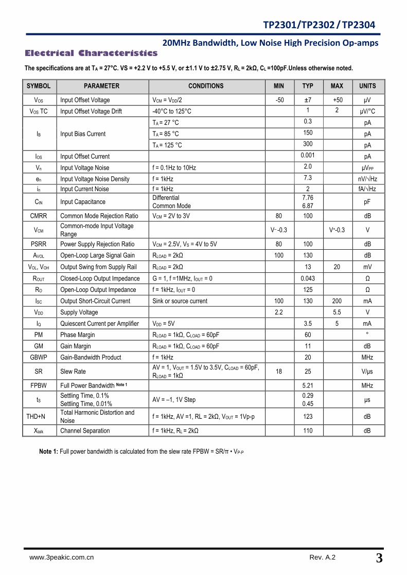
Electrical Characteristics
The specifications are at TA = 27° C. VS = +2.2 V to +5.5 V, or ± 1.1 V to ± 2.75 V, RL = 2kΩ, CL =100pF.Unless otherwise noted.
SYMBOL PARAMETER CONDITIONS MIN TYP MAX UNITS
VOS Input Offset Voltage VCM = VDD/2 -50 ± 7 +50 μV
VOS TC Input Offset Voltage Drift -40° C to 125° C 1 2 μV/° C
IB Input Bias Current
TA = 27 ° C 0.3 pA
TA = 85 ° C 150 pA
TA = 125 ° C 300 pA
IOS Input Offset Current 0.001 pA
Vn Input Voltage Noise f = 0.1Hz to 10Hz 2.0 μVPP
en Input Voltage Noise Density f = 1kHz 7.3 nV/√Hz
in Input Current Noise f = 1kHz 2 fA/√Hz
CIN Input Capacitance Differential
Common Mode
7.76
6.87 pF
CMRR Common Mode Rejection Ratio VCM = 2V to 3V 80 100 dB
VCM Common-mode Input Voltage
Range V– -0.3 V+-0.3 V
PSRR Power Supply Rejection Ratio VCM = 2.5V, VS = 4V to 5V 80 100 dB
AVOL Open-Loop Large Signal Gain RLOAD = 2kΩ 100 130 dB
VOL, VOH Output Swing from Supply Rail RLOAD = 2kΩ 13 20 mV
ROUT Closed-Loop Output Impedance G = 1, f =1MHz, IOUT = 0 0.043 Ω
RO Open-Loop Output Impedance f = 1kHz, IOUT = 0 125 Ω
ISC Output Short-Circuit Current Sink or source current 100 130 200 mA
VDD Supply Voltage 2.2 5.5 V
IQ Quiescent Current per Amplifier VDD = 5V 3.5 5 mA
PM Phase Margin RLOAD = 1kΩ, CLOAD = 60pF 60 °
GM Gain Margin RLOAD = 1kΩ, CLOAD = 60pF 11 dB
GBWP Gain-Bandwidth Product f = 1kHz 20 MHz
SR Slew Rate AV = 1, VOUT = 1.5V to 3.5V, CLOAD = 60pF,
RLOAD = 1kΩ 18 25 V/μs
FPBW Full Power Bandwidth Note 1 5.21 MHz
tS Settling Time, 0.1%
Settling Time, 0.01% AV = –1, 1V Step
0.29
0.45 μs
THD+N Total Harmonic Distortion and
Noise f = 1kHz, AV =1, RL = 2kΩ, VOUT = 1Vp-p 123 dB
Xtalk Channel Separation f = 1kHz, RL = 2kΩ 110 dB
Note 1: Full power bandwidth is calculated from the slew rate FPBW = SR/π • VP-P
4 Rev.A.2
www.3peakic.com.cn
TP2301 / TP2302 / TP2304
20MHz Bandwidth, Low Noise High Precision Op-amps
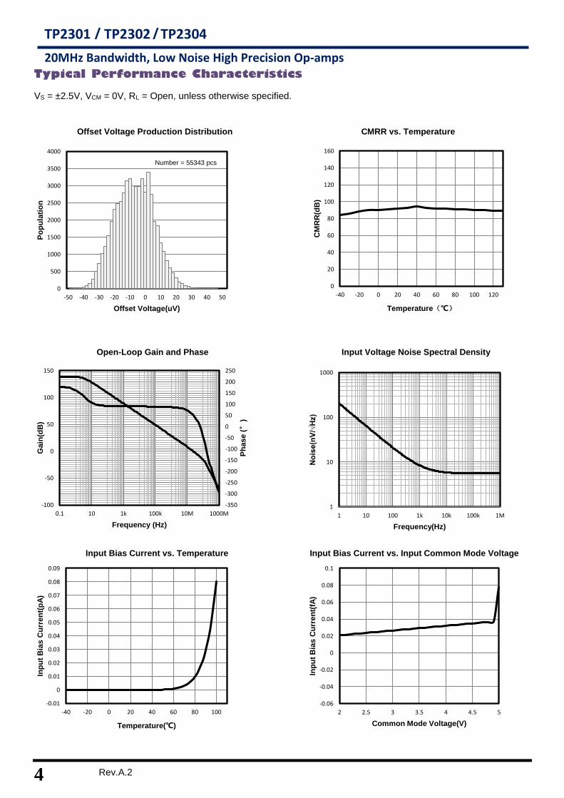
Typical Performance Characteristics
VS = ±2.5V, VCM = 0V, RL = Open, unless otherwise specified.
Offset Voltage Production Distribution CMRR vs. Temperature
Open-Loop Gain and Phase Input Voltage Noise Spectral Density
Input Bias Current vs. Temperature Input Bias Current vs. Input Common Mode Voltage
0
500
1000
1500
2000
2500
3000
3500
4000
-50 -40 -30 -20 -10 0 10 20 30 40 50
Po
pu
lati
on
Offset Voltage(uV)
Number = 55343 pcs
0
20
40
60
80
100
120
140
160
-40 -20 0 20 40 60 80 100 120
CM
RR
(dB
)Temperature(℃)
-350
-300
-250
-200
-150
-100
-50
0
50
100
150
200
250
-100
-50
0
50
100
150
0.1 10 1k 100k 10M 1000M
Ph
ase (°
)
Gain
(dB
)
Frequency (Hz)
1
10
100
1000
1 10 100 1k 10k 100k 1M
Noise(nV/√Hz)
Frequency(Hz)
-0.01
0
0.01
0.02
0.03
0.04
0.05
0.06
0.07
0.08
0.09
-40 -20 0 20 40 60 80 100
Inp
ut
Bia
s C
urr
en
t(p
A)
Temperature(℃)
-0.06
-0.04
-0.02
0
0.02
0.04
0.06
0.08
0.1
2 2.5 3 3.5 4 4.5 5
Inp
ut
Bia
s C
urr
en
t(fA
)
Common Mode Voltage(V)
5
TP2301/TP2302 / TP2304
20MHz Bandwidth, Low Noise High Precision Op-amps
www.3peakic.com.cn Rev. A.2
Typical Performance Characteristics
VS = ±2.5V, VCM = 0V, RL = Open, unless otherwise specified. (Continued)
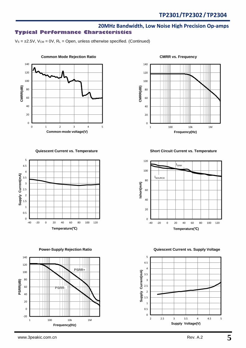
Common Mode Rejection Ratio CMRR vs. Frequency
Quiescent Current vs. Temperature Short Circuit Current vs. Temperature
Power-Supply Rejection Ratio Quiescent Current vs. Supply Voltage
0
20
40
60
80
100
120
140
0 1 2 3 4 5
CM
RR
(dB
)
Common-mode voltage(V)
0
20
40
60
80
100
120
140
1 100 10k 1M
CM
RR
(dB
)
Frequency(Hz)
0
0.5
1
1.5
2
2.5
3
3.5
4
4.5
5
-40 -20 0 20 40 60 80 100 120
Su
pp
ly
Cu
rren
t(m
A)
Temperature(℃)
0
20
40
60
80
100
120
-40 -20 0 20 40 60 80 100 120
Ish
ort
(mA
)
Temperature(℃)
ISINK
ISOURCE
-20
0
20
40
60
80
100
120
140
1 100 10k 1M
PS
RR
(dB
)
Frequency(Hz)
PSRR+
PSRR-
0
0.5
1
1.5
2
2.5
3
3.5
4
4.5
5
2 2.5 3 3.5 4 4.5 5
Su
pp
ly
Cu
rren
t(m
A)
Supply Voltage(V)
6 Rev.A.2
www.3peakic.com.cn
TP2301 / TP2302 / TP2304
20MHz Bandwidth, Low Noise High Precision Op-amps
Typical Performance Characteristics
VS = ±2.5V, VCM = 0V, RL = Open, unless otherwise specified. (Continued)
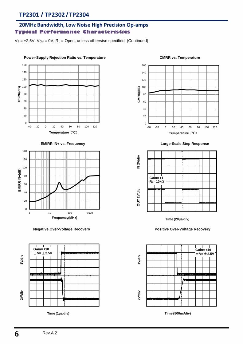
Power-Supply Rejection Ratio vs. Temperature CMRR vs. Temperature
EMIRR IN+ vs. Frequency Large-Scale Step Response
Negative Over-Voltage Recovery Positive Over-Voltage Recovery
0
20
40
60
80
100
120
140
160
-40 -20 0 20 40 60 80 100 120
PS
RR
(dB
)
Temperature(℃)
0
20
40
60
80
100
120
140
160
-40 -20 0 20 40 60 80 100 120
CM
RR
(dB
)
Temperature(℃)
0
20
40
60
80
100
120
140
1 10 100 1000
EM
IRR
IN
+(d
B)
Frequency(MHz) Time (20µs/div)
OU
T 2
V/d
iv
IN
2V
/div
Gain= +1RL= 10kΩ
2V
/div
1V
/div
Time (1µs/div)
Gain= +10
±V= ±2.5V
2V
/div
1V
/div
Time (500ns/div)
Gain= +10
±V= ±2.5V
7
TP2301/TP2302 / TP2304
20MHz Bandwidth, Low Noise High Precision Op-amps
www.3peakic.com.cn Rev. A.2
Typical Performance Characteristics
VS = ±2.5V, VCM = 0V, RL = Open, unless otherwise specified. (Continued)
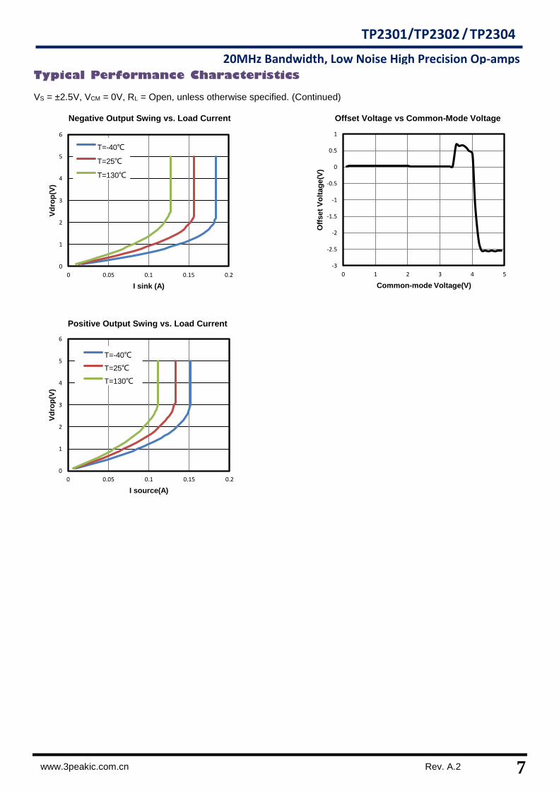
Negative Output Swing vs. Load Current Offset Voltage vs Common-Mode Voltage
Positive Output Swing vs. Load Current
0
1
2
3
4
5
6
0 0.05 0.1 0.15 0.2
Vd
rop
(V)
I sink (A)
T=-40℃
T=25℃
T=130℃
-3
-2.5
-2
-1.5
-1
-0.5
0
0.5
1
0 1 2 3 4 5
Off
set
Vo
ltag
e(V
)
Common-mode Voltage(V)
0
1
2
3
4
5
6
0 0.05 0.1 0.15 0.2
Vd
rop
(V)
I source(A)
T=-40℃
T=25℃
T=130℃
8 Rev.A.2
www.3peakic.com.cn
TP2301 / TP2302 / TP2304
20MHz Bandwidth, Low Noise High Precision Op-amps
Pin Functions
-IN: Inverting Input of the Amplifier.
+IN: Non-Inverting Input of Amplifier.
OUT: Amplifier Output. The voltage range extends to
within mV of each supply rail.
V+ or +Vs: Positive Power Supply. Typically the voltage
is from 2.2V to 5.5V. Split supplies are possible as long
as the voltage between V+ and V– is between 2.2V and
5.5V. A bypass capacitor of 0.1μF as close to the part as
possible should be used between power supply pins or
between supply pins and ground.
V- or -Vs: Negative Power Supply. It is normally tied to
ground. It can also be tied to a voltage other than
ground as long as the voltage between V+ and V– is from
2.2V to 5.5V. If it is not connected to ground, bypass it
with a capacitor of 0.1μF as close to the part as
possible.
Operation
The TP2301 series op amps can operate on a single-supply voltage (2.2 V to 5.5 V), or a split-supply voltage (±1.1 V to
±2.75 V), making them highly versatile and easy to use. The power-supply pins should have local bypass ceramic
capacitors (typically 0.001 μF to 0.1 μF). These amplifiers are fully specified from +2.2 V to +5.5 V and over the
extended temperature range of –40°C to +125°C. Parameters that can exhibit variance with regard to operating voltage
or temperature are presented in the Typical Characteristics
Applications Information
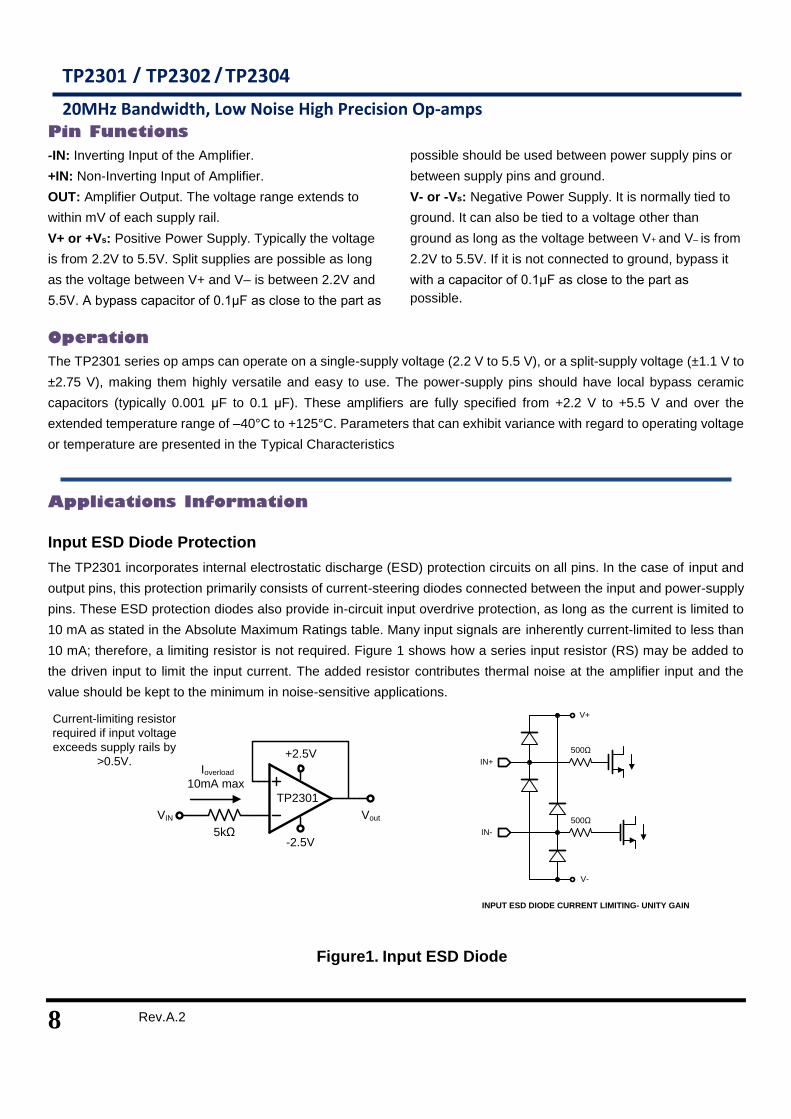
Input ESD Diode Protection
The TP2301 incorporates internal electrostatic discharge (ESD) protection circuits on all pins. In the case of input and
output pins, this protection primarily consists of current-steering diodes connected between the input and power-supply
pins. These ESD protection diodes also provide in-circuit input overdrive protection, as long as the current is limited to
10 mA as stated in the Absolute Maximum Ratings table. Many input signals are inherently current-limited to less than
10 mA; therefore, a limiting resistor is not required. Figure 1 shows how a series input resistor (RS) may be added to
the driven input to limit the input current. The added resistor contributes thermal noise at the amplifier input and the
value should be kept to the minimum in noise-sensitive applications.
IN+
IN-
V+
V-
500Ω
500Ω
INPUT ESD DIODE CURRENT LIMITING- UNITY GAIN
Figure1. Input ESD Diode
Ioverload
10mA max
VIN
Current-limiting resistor
required if input voltage
exceeds supply rails by
>0.5V.
TP2301
Vout
+2.5V
-2.5V5kΩ
9
TP2301/TP2302 / TP2304
20MHz Bandwidth, Low Noise High Precision Op-amps
www.3peakic.com.cn Rev. A.2
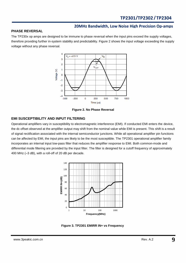
PHASE REVERSAL
The TP230x op amps are designed to be immune to phase reversal when the input pins exceed the supply voltages,
therefore providing further in-system stability and predictability. Figure 2 shows the input voltage exceeding the supply
voltage without any phase reversal.
Figure 2. No Phase Reversal
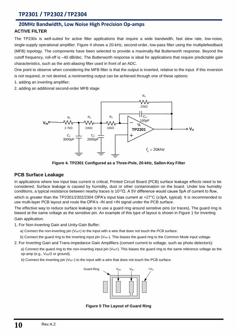
EMI SUSCEPTIBILITY AND INPUT FILTERING
Operational amplifiers vary in susceptibility to electromagnetic interference (EMI). If conducted EMI enters the device,
the dc offset observed at the amplifier output may shift from the nominal value while EMI is present. This shift is a result
of signal rectification associated with the internal semiconductor junctions. While all operational amplifier pin functions
can be affected by EMI, the input pins are likely to be the most susceptible. The TP2301 operational amplifier family
incorporates an internal input low-pass filter that reduces the amplifier response to EMI. Both common-mode and
differential mode filtering are provided by the input filter. The filter is designed for a cutoff frequency of approximately
400 MHz (–3 dB), with a roll-off of 20 dB per decade.
Figure 3. TP2301 EMIRR IN+ vs Frequency
0
20
40
60
80
100
120
140
1 10 100 1000
EM
IRR
IN
+(d
B)
Frequency(MHz)
10 Rev.A.2
www.3peakic.com.cn
TP2301 / TP2302 / TP2304
20MHz Bandwidth, Low Noise High Precision Op-amps
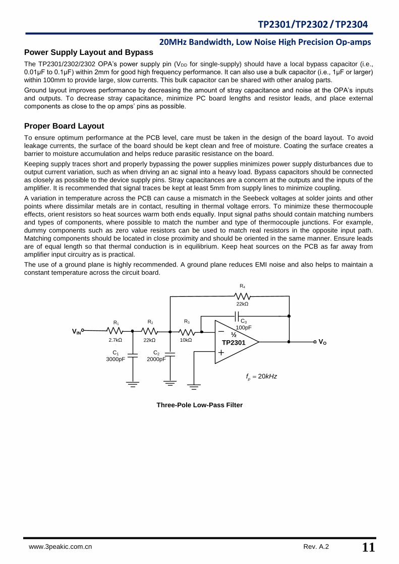
ACTIVE FILTER
The TP230x is well-suited for active filter applications that require a wide bandwidth, fast slew rate, low-noise,
single-supply operational amplifier. Figure 4 shows a 20-kHz, second-order, low-pass filter using the multiplefeedback
(MFB) topology. The components have been selected to provide a maximally-flat Butterworth response. Beyond the
cutoff frequency, roll-off is –40 dB/dec. The Butterworth response is ideal for applications that require predictable gain
characteristics, such as the anti-aliasing filter used in front of an ADC.
One point to observe when considering the MFB filter is that the output is inverted, relative to the input. If this inversion
is not required, or not desired, a noninverting output can be achieved through one of these options:
1. adding an inverting amplifier;
2. adding an additional second-order MFB stage
½
TP2301
VIN
C1
3000pF
R2
22kΩ
22kΩ
R4
R1
2.7kΩ 10kΩ
R3 C3
100pF
VO
C2
2000pF
20pf kHz
Figure 4. TP2301 Configured as a Three-Pole, 20-kHz, Sallen-Key Filter
PCB Surface Leakage
In applications where low input bias current is critical, Printed Circuit Board (PCB) surface leakage effects need to be
considered. Surface leakage is caused by humidity, dust or other contamination on the board. Under low humidity
conditions, a typical resistance between nearby traces is 1012Ω. A 5V difference would cause 5pA of current to flow,
which is greater than the TP2301/2302/2304 OPA’s input bias current at +27°C (±3pA, typical). It is recommended to
use multi-layer PCB layout and route the OPA’s -IN and +IN signal under the PCB surface.
The effective way to reduce surface leakage is to use a guard ring around sensitive pins (or traces). The guard ring is
biased at the same voltage as the sensitive pin. An example of this type of layout is shown in Figure 1 for Inverting
Gain application.
1. For Non-Inverting Gain and Unity-Gain Buffer:
a) Connect the non-inverting pin (VIN+) to the input with a wire that does not touch the PCB surface.
b) Connect the guard ring to the inverting input pin (VIN–). This biases the guard ring to the Common Mode input voltage.
2. For Inverting Gain and Trans-impedance Gain Amplifiers (convert current to voltage, such as photo detectors):
a) Connect the guard ring to the non-inverting input pin (VIN+). This biases the guard ring to the same reference voltage as the
op-amp (e.g., VDD/2 or ground).
b) Connect the inverting pin (VIN–) to the input with a wire that does not touch the PCB surface.
VIN+ VIN- +VSGuard Ring
Figure 5 The Layout of Guard Ring
11
TP2301/TP2302 / TP2304
20MHz Bandwidth, Low Noise High Precision Op-amps
www.3peakic.com.cn Rev. A.2
Power Supply Layout and Bypass
The TP2301/2302/2302 OPA’s power supply pin (VDD for single-supply) should have a local bypass capacitor (i.e.,
0.01μF to 0.1μF) within 2mm for good high frequency performance. It can also use a bulk capacitor (i.e., 1μF or larger)
within 100mm to provide large, slow currents. This bulk capacitor can be shared with other analog parts.
Ground layout improves performance by decreasing the amount of stray capacitance and noise at the OPA’s inputs
and outputs. To decrease stray capacitance, minimize PC board lengths and resistor leads, and place external
components as close to the op amps’ pins as possible.
Proper Board Layout
To ensure optimum performance at the PCB level, care must be taken in the design of the board layout. To avoid
leakage currents, the surface of the board should be kept clean and free of moisture. Coating the surface creates a
barrier to moisture accumulation and helps reduce parasitic resistance on the board.
Keeping supply traces short and properly bypassing the power supplies minimizes power supply disturbances due to
output current variation, such as when driving an ac signal into a heavy load. Bypass capacitors should be connected
as closely as possible to the device supply pins. Stray capacitances are a concern at the outputs and the inputs of the
amplifier. It is recommended that signal traces be kept at least 5mm from supply lines to minimize coupling.
A variation in temperature across the PCB can cause a mismatch in the Seebeck voltages at solder joints and other
points where dissimilar metals are in contact, resulting in thermal voltage errors. To minimize these thermocouple
effects, orient resistors so heat sources warm both ends equally. Input signal paths should contain matching numbers
and types of components, where possible to match the number and type of thermocouple junctions. For example,
dummy components such as zero value resistors can be used to match real resistors in the opposite input path.
Matching components should be located in close proximity and should be oriented in the same manner. Ensure leads
are of equal length so that thermal conduction is in equilibrium. Keep heat sources on the PCB as far away from
amplifier input circuitry as is practical.
The use of a ground plane is highly recommended. A ground plane reduces EMI noise and also helps to maintain a
constant temperature across the circuit board.
½
TP2301
VIN
C1
3000pF
R2
22kΩ
22kΩ
R4
R1
2.7kΩ 10kΩ
R3 C3
100pF
VO
C2
2000pF
20pf kHz
Three-Pole Low-Pass Filter
12 Rev.A.2
www.3peakic.com.cn
TP2301 / TP2302 / TP2304
20MHz Bandwidth, Low Noise High Precision Op-amps
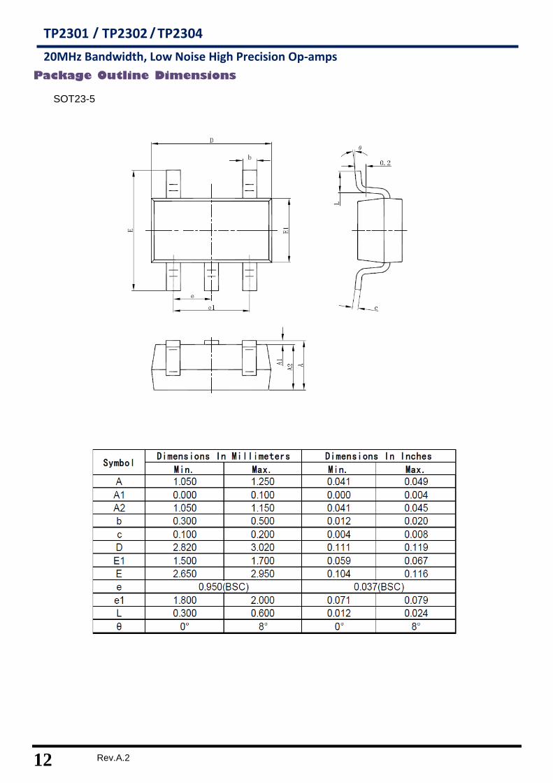
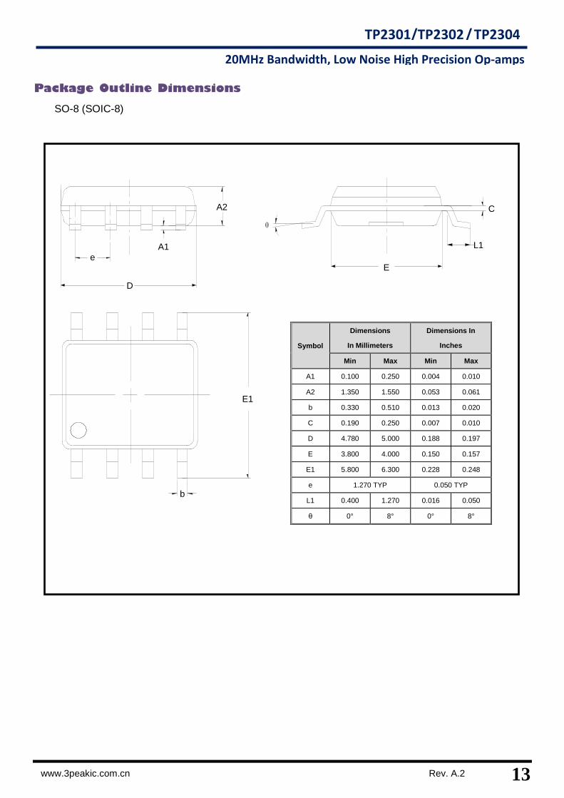
Package Outline Dimensions
SOT23-5
13
TP2301/TP2302 / TP2304
20MHz Bandwidth, Low Noise High Precision Op-amps
www.3peakic.com.cn Rev. A.2
D
E1
b
E
A1
A2
e
θ
L1
C
Package Outline Dimensions
SO-8 (SOIC-8)
Symbol
Dimensions
In Millimeters
Dimensions In
Inches
Min Max Min Max
A1 0.100 0.250 0.004 0.010
A2 1.350 1.550 0.053 0.061
b 0.330 0.510 0.013 0.020
C 0.190 0.250 0.007 0.010
D 4.780 5.000 0.188 0.197
E 3.800 4.000 0.150 0.157
E1 5.800 6.300 0.228 0.248
e 1.270 TYP 0.050 TYP
L1 0.400 1.270 0.016 0.050
θ 0° 8° 0° 8°
14 Rev.A.2
www.3peakic.com.cn
TP2301 / TP2302 / TP2304
20MHz Bandwidth, Low Noise High Precision Op-amps
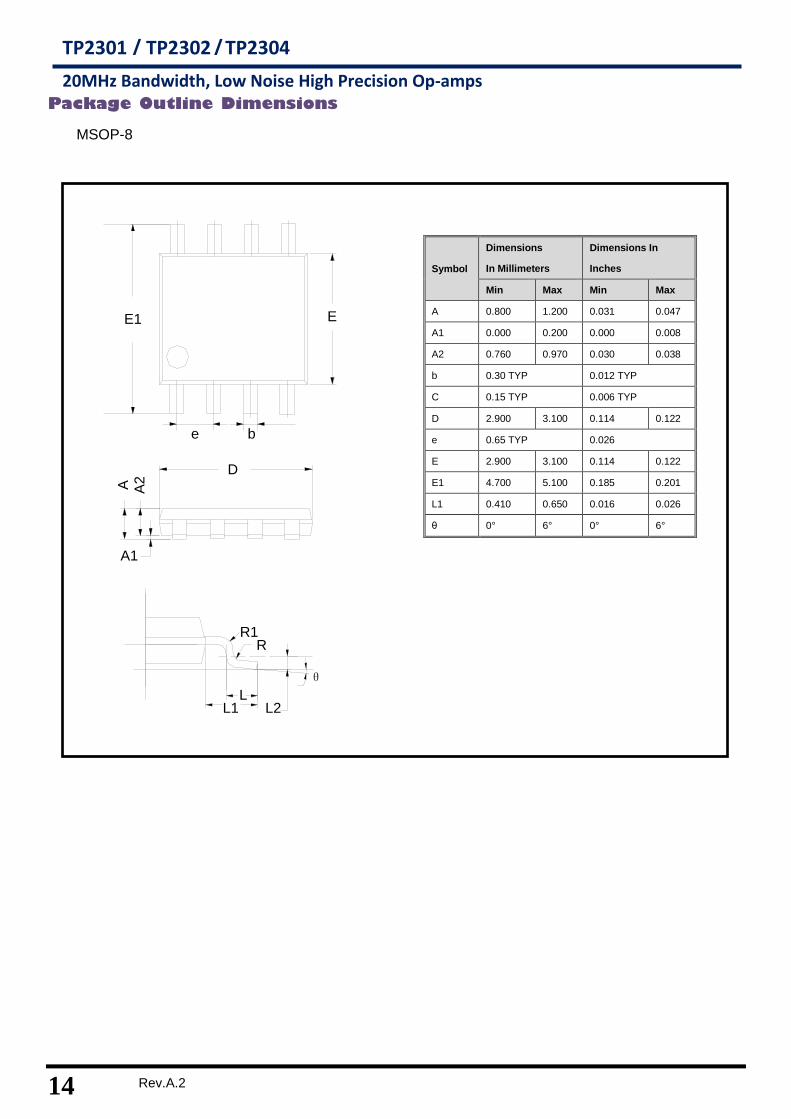
Package Outline Dimensions
MSOP-8
Symbol
Dimensions
In Millimeters
Dimensions In
Inches
Min Max Min Max
A 0.800 1.200 0.031 0.047
A1 0.000 0.200 0.000 0.008
A2 0.760 0.970 0.030 0.038
b 0.30 TYP 0.012 TYP
C 0.15 TYP 0.006 TYP
D 2.900 3.100 0.114 0.122
e 0.65 TYP 0.026
E 2.900 3.100 0.114 0.122
E1 4.700 5.100 0.185 0.201
L1 0.410 0.650 0.016 0.026
θ 0° 6° 0° 6°
E1
e
E
A1
A2A
D
L1 L2L
RR1
θ
b
15
TP2301/TP2302 / TP2304
20MHz Bandwidth, Low Noise High Precision Op-amps
www.3peakic.com.cn Rev. A.2
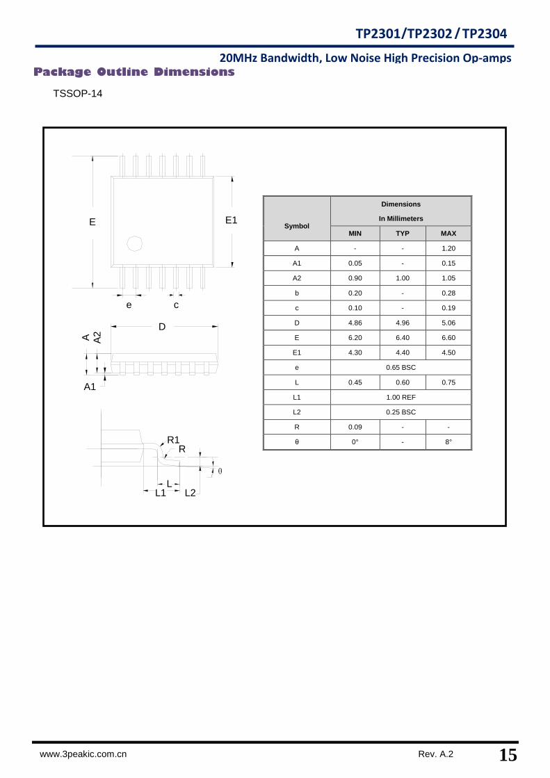
Package Outline Dimensions
TSSOP-14
Symbol
Dimensions
In Millimeters
MIN TYP MAX
A - - 1.20
A1 0.05 - 0.15
A2 0.90 1.00 1.05
b 0.20 - 0.28
c 0.10 - 0.19
D 4.86 4.96 5.06
E 6.20 6.40 6.60
E1 4.30 4.40 4.50
e 0.65 BSC
L 0.45 0.60 0.75
L1 1.00 REF
L2 0.25 BSC
R 0.09 - -
θ 0° - 8°
E
e
E1
A1
A2A
D
L1 L2L
RR1
θ
c
16 Rev.A.2
www.3peakic.com.cn
TP2301 / TP2302 / TP2304
20MHz Bandwidth, Low Noise High Precision Op-amps
θ
e b
E1 E
D
A1
A A2
L1L
L2
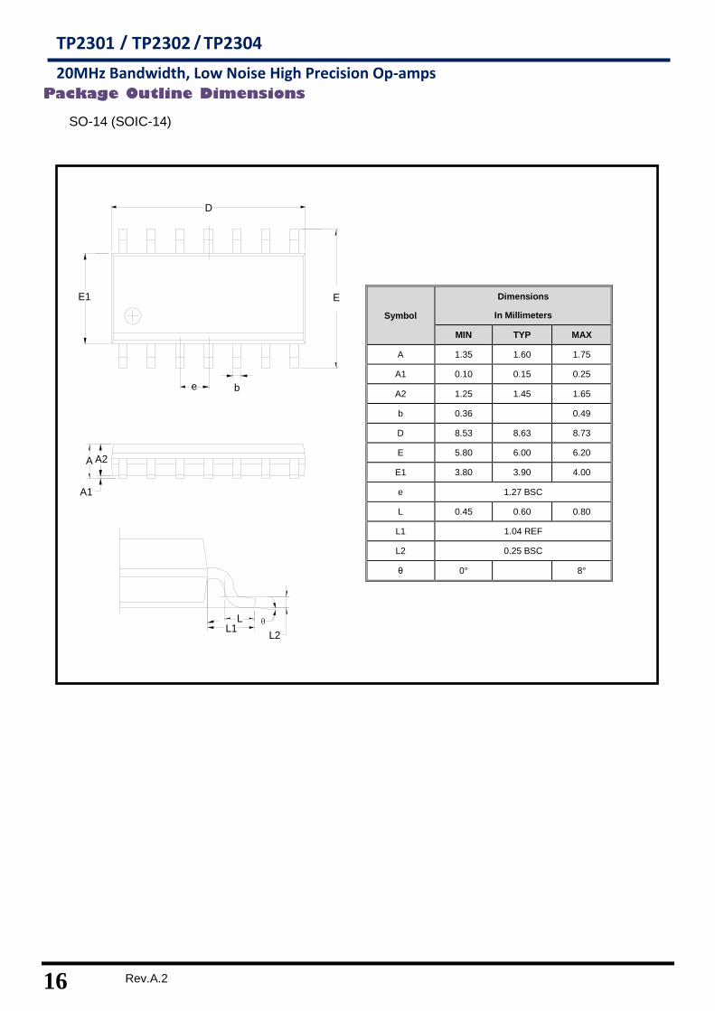
Package Outline Dimensions
SO-14 (SOIC-14)
Symbol
Dimensions
In Millimeters
MIN TYP MAX
A 1.35 1.60 1.75
A1 0.10 0.15 0.25
A2 1.25 1.45 1.65
b 0.36 0.49
D 8.53 8.63 8.73
E 5.80 6.00 6.20
E1 3.80 3.90 4.00
e 1.27 BSC
L 0.45 0.60 0.80
L1 1.04 REF
L2 0.25 BSC
θ 0° 8°