SNOSBD8E – MAY 2004– REVISED …aitendo3.sakura.ne.jp/aitendo_data/product_img/ic/OpAmp...Op...
25
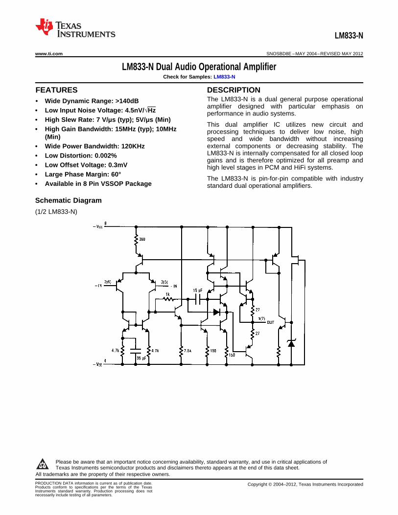
LM833-N www.ti.com SNOSBD8E – MAY 2004 – REVISED MAY 2012 LM833-N Dual Audio Operational Amplifier Check for Samples: LM833-N 1FEATURES DESCRIPTION The LM833-N is a dual general purpose operational 2• Wide Dynamic Range: >140dB amplifier designed with particular emphasis on • Low Input Noise Voltage: 4.5nV/√Hz performance in audio systems. • High Slew Rate: 7 V/μs (typ); 5V/μs (Min) This dual amplifier IC utilizes new circuit and • High Gain Bandwidth: 15MHz (typ); 10MHz processing techniques to deliver low noise, high (Min) speed and wide bandwidth without increasing external components or decreasing stability. The • Wide Power Bandwidth: 120KHz LM833-N is internally compensated for all closed loop • Low Distortion: 0.002% gains and is therefore optimized for all preamp and • Low Offset Voltage: 0.3mV high level stages in PCM and HiFi systems. • Large Phase Margin: 60° The LM833-N is pin-for-pin compatible with industry • Available in 8 Pin VSSOP Package standard dual operational amplifiers. Schematic Diagram (1/2 LM833-N) 1 Please be aware that an important notice concerning availability, standard warranty, and use in critical applications of Texas Instruments semiconductor products and disclaimers thereto appears at the end of this data sheet. 2All trademarks are the property of their respective owners. PRODUCTION DATA information is current as of publication date. Copyright © 2004–2012, Texas Instruments Incorporated Products conform to specifications per the terms of the Texas Instruments standard warranty. Production processing does not necessarily include testing of all parameters.
Transcript of SNOSBD8E – MAY 2004– REVISED …aitendo3.sakura.ne.jp/aitendo_data/product_img/ic/OpAmp...Op...
LM833-N
www.ti.com SNOSBD8E –MAY 2004–REVISED MAY 2012
LM833-N Dual Audio Operational AmplifierCheck for Samples: LM833-N
1FEATURES DESCRIPTIONThe LM833-N is a dual general purpose operational
2• Wide Dynamic Range: >140dBamplifier designed with particular emphasis on
• Low Input Noise Voltage: 4.5nV/√Hz performance in audio systems.• High Slew Rate: 7 V/μs (typ); 5V/μs (Min)
This dual amplifier IC utilizes new circuit and• High Gain Bandwidth: 15MHz (typ); 10MHz processing techniques to deliver low noise, high
(Min) speed and wide bandwidth without increasingexternal components or decreasing stability. The• Wide Power Bandwidth: 120KHzLM833-N is internally compensated for all closed loop• Low Distortion: 0.002%gains and is therefore optimized for all preamp and
• Low Offset Voltage: 0.3mV high level stages in PCM and HiFi systems.• Large Phase Margin: 60°
The LM833-N is pin-for-pin compatible with industry• Available in 8 Pin VSSOP Package standard dual operational amplifiers.
Schematic Diagram
(1/2 LM833-N)
1
Please be aware that an important notice concerning availability, standard warranty, and use in critical applications ofTexas Instruments semiconductor products and disclaimers thereto appears at the end of this data sheet.
2All trademarks are the property of their respective owners.
PRODUCTION DATA information is current as of publication date. Copyright © 2004–2012, Texas Instruments IncorporatedProducts conform to specifications per the terms of the TexasInstruments standard warranty. Production processing does notnecessarily include testing of all parameters.
LM833-N
SNOSBD8E –MAY 2004–REVISED MAY 2012 www.ti.com
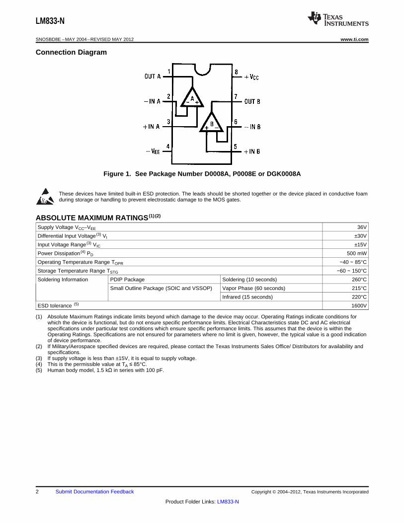
Connection Diagram
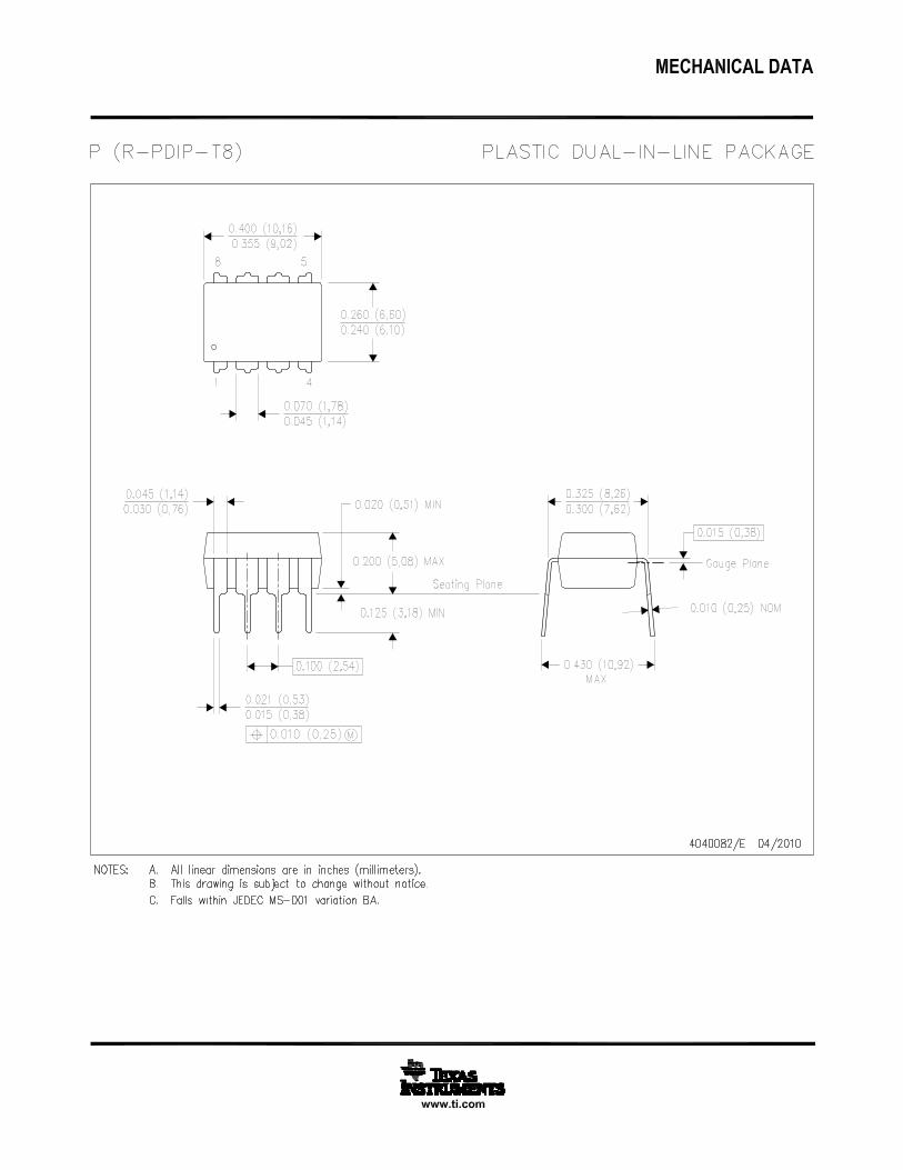
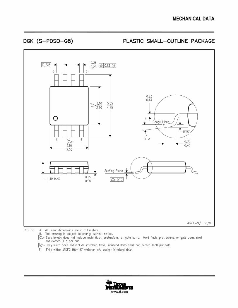
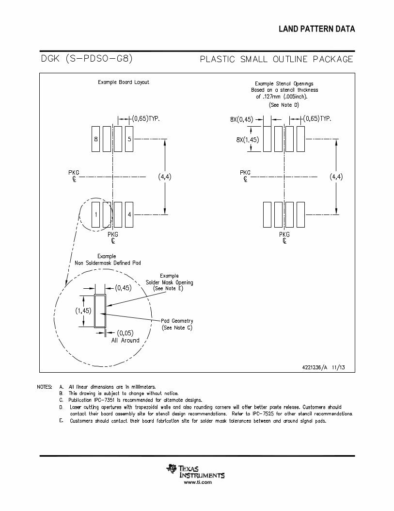
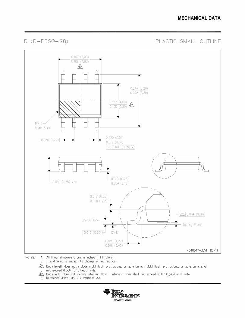
Figure 1. See Package Number D0008A, P0008E or DGK0008A
These devices have limited built-in ESD protection. The leads should be shorted together or the device placed in conductive foamduring storage or handling to prevent electrostatic damage to the MOS gates.
ABSOLUTE MAXIMUM RATINGS (1) (2)
Supply Voltage VCC–VEE 36V
Differential Input Voltage (3) VI ±30V
Input Voltage Range (3) VIC ±15V
Power Dissipation (4) PD 500 mW
Operating Temperature Range TOPR −40 ∼ 85°C
Storage Temperature Range TSTG −60 ∼ 150°C
Soldering Information PDIP Package Soldering (10 seconds) 260°C
Small Outline Package (SOIC and VSSOP) Vapor Phase (60 seconds) 215°C
Infrared (15 seconds) 220°C
ESD tolerance (5) 1600V
(1) Absolute Maximum Ratings indicate limits beyond which damage to the device may occur. Operating Ratings indicate conditions forwhich the device is functional, but do not ensure specific performance limits. Electrical Characteristics state DC and AC electricalspecifications under particular test conditions which ensure specific performance limits. This assumes that the device is within theOperating Ratings. Specifications are not ensured for parameters where no limit is given, however, the typical value is a good indicationof device performance.
(2) If Military/Aerospace specified devices are required, please contact the Texas Instruments Sales Office/ Distributors for availability andspecifications.
(3) If supply voltage is less than ±15V, it is equal to supply voltage.(4) This is the permissible value at TA ≤ 85°C.(5) Human body model, 1.5 kΩ in series with 100 pF.
2 Submit Documentation Feedback Copyright © 2004–2012, Texas Instruments Incorporated
Product Folder Links: LM833-N
LM833-N
www.ti.com SNOSBD8E –MAY 2004–REVISED MAY 2012
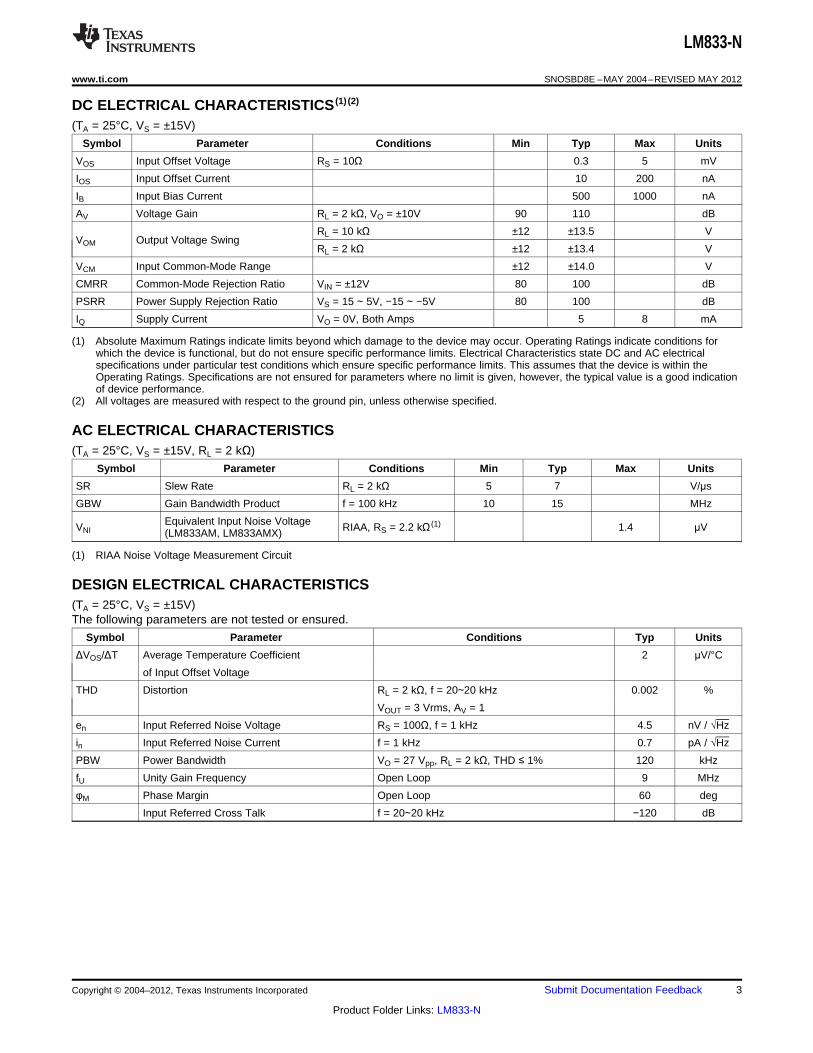
DC ELECTRICAL CHARACTERISTICS (1) (2)
(TA = 25°C, VS = ±15V)
Symbol Parameter Conditions Min Typ Max Units
VOS Input Offset Voltage RS = 10Ω 0.3 5 mV
IOS Input Offset Current 10 200 nA
IB Input Bias Current 500 1000 nA
AV Voltage Gain RL = 2 kΩ, VO = ±10V 90 110 dB
RL = 10 kΩ ±12 ±13.5 VVOM Output Voltage Swing
RL = 2 kΩ ±12 ±13.4 V
VCM Input Common-Mode Range ±12 ±14.0 V
CMRR Common-Mode Rejection Ratio VIN = ±12V 80 100 dB
PSRR Power Supply Rejection Ratio VS = 15 ∼ 5V, −15 ∼ −5V 80 100 dB
IQ Supply Current VO = 0V, Both Amps 5 8 mA
(1) Absolute Maximum Ratings indicate limits beyond which damage to the device may occur. Operating Ratings indicate conditions forwhich the device is functional, but do not ensure specific performance limits. Electrical Characteristics state DC and AC electricalspecifications under particular test conditions which ensure specific performance limits. This assumes that the device is within theOperating Ratings. Specifications are not ensured for parameters where no limit is given, however, the typical value is a good indicationof device performance.
(2) All voltages are measured with respect to the ground pin, unless otherwise specified.
AC ELECTRICAL CHARACTERISTICS(TA = 25°C, VS = ±15V, RL = 2 kΩ)
Symbol Parameter Conditions Min Typ Max Units
SR Slew Rate RL = 2 kΩ 5 7 V/μs
GBW Gain Bandwidth Product f = 100 kHz 10 15 MHz
Equivalent Input Noise VoltageVNI RIAA, RS = 2.2 kΩ (1) 1.4 μV(LM833AM, LM833AMX)
(1) RIAA Noise Voltage Measurement Circuit
DESIGN ELECTRICAL CHARACTERISTICS(TA = 25°C, VS = ±15V)The following parameters are not tested or ensured.
Symbol Parameter Conditions Typ Units
ΔVOS/ΔT Average Temperature Coefficient 2 μV/°C
of Input Offset Voltage
THD Distortion RL = 2 kΩ, f = 20∼20 kHz 0.002 %
VOUT = 3 Vrms, AV = 1
en Input Referred Noise Voltage RS = 100Ω, f = 1 kHz 4.5 nV / √Hz
in Input Referred Noise Current f = 1 kHz 0.7 pA / √Hz
PBW Power Bandwidth VO = 27 Vpp, RL = 2 kΩ, THD ≤ 1% 120 kHz
fU Unity Gain Frequency Open Loop 9 MHz
φM Phase Margin Open Loop 60 deg
Input Referred Cross Talk f = 20∼20 kHz −120 dB
Copyright © 2004–2012, Texas Instruments Incorporated Submit Documentation Feedback 3
Product Folder Links: LM833-N

LM833-N
SNOSBD8E –MAY 2004–REVISED MAY 2012 www.ti.com
TYPICAL PERFORMANCE CHARACTERISTICS
Maximum Power Input Bias Current vsDissipation Ambient Temperature
vs Ambient Temperature
Figure 2. Figure 3.
Input Bias Current vsSupply Voltage Supply Current vs
Supply Voltage
Figure 4. Figure 5.
DC Voltage Gain DC Voltage Gainvs Ambient Temperature vs Supply Voltage
Figure 6. Figure 7.
4 Submit Documentation Feedback Copyright © 2004–2012, Texas Instruments Incorporated
Product Folder Links: LM833-N
LM833-N
www.ti.com SNOSBD8E –MAY 2004–REVISED MAY 2012
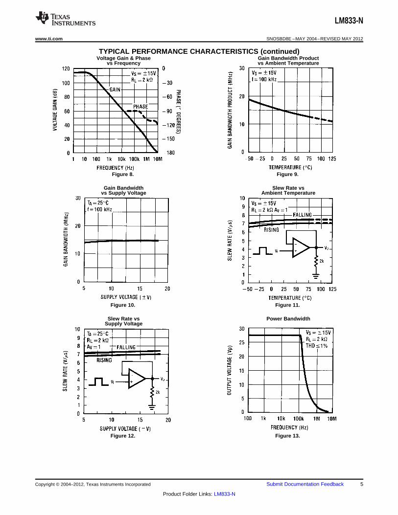
TYPICAL PERFORMANCE CHARACTERISTICS (continued)Voltage Gain & Phase Gain Bandwidth Product
vs Frequency vs Ambient Temperature
Figure 8. Figure 9.
Gain Bandwidth Slew Rate vsvs Supply Voltage Ambient Temperature
Figure 10. Figure 11.
Slew Rate vs Power BandwidthSupply Voltage
Figure 12. Figure 13.
Copyright © 2004–2012, Texas Instruments Incorporated Submit Documentation Feedback 5
Product Folder Links: LM833-N
LM833-N
SNOSBD8E –MAY 2004–REVISED MAY 2012 www.ti.com
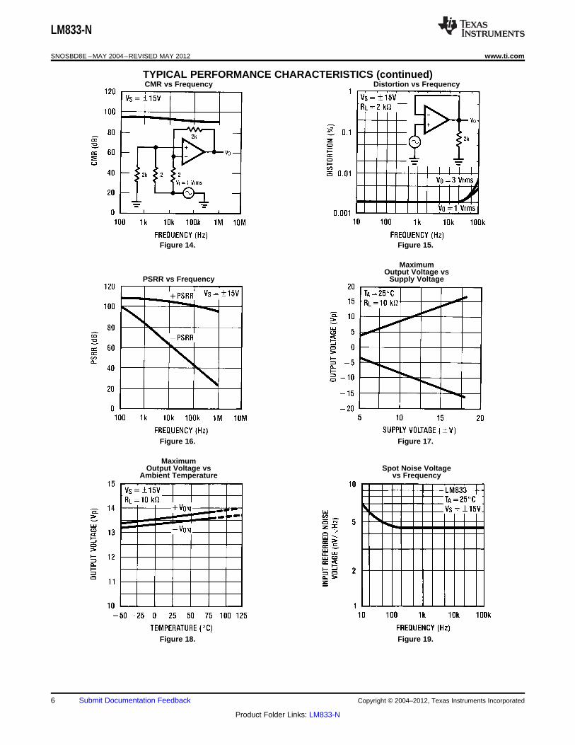
TYPICAL PERFORMANCE CHARACTERISTICS (continued)CMR vs Frequency Distortion vs Frequency
Figure 14. Figure 15.
MaximumOutput Voltage vs
PSRR vs Frequency Supply Voltage
Figure 16. Figure 17.
MaximumOutput Voltage vs Spot Noise Voltage
Ambient Temperature vs Frequency
Figure 18. Figure 19.
6 Submit Documentation Feedback Copyright © 2004–2012, Texas Instruments Incorporated
Product Folder Links: LM833-N
LM833-N
www.ti.com SNOSBD8E –MAY 2004–REVISED MAY 2012
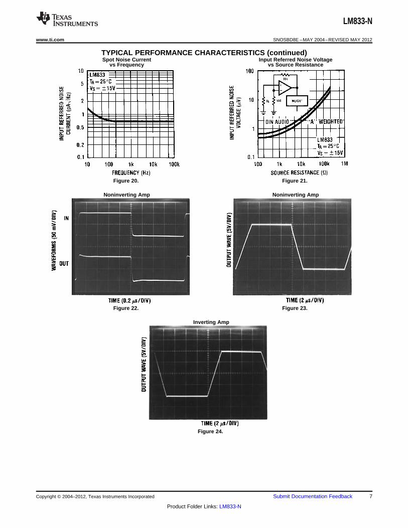
TYPICAL PERFORMANCE CHARACTERISTICS (continued)Spot Noise Current Input Referred Noise Voltage
vs Frequency vs Source Resistance
Figure 20. Figure 21.
Noninverting Amp Noninverting Amp
Figure 22. Figure 23.
Inverting Amp
Figure 24.
Copyright © 2004–2012, Texas Instruments Incorporated Submit Documentation Feedback 7
Product Folder Links: LM833-N
LM833-N
SNOSBD8E –MAY 2004–REVISED MAY 2012 www.ti.com
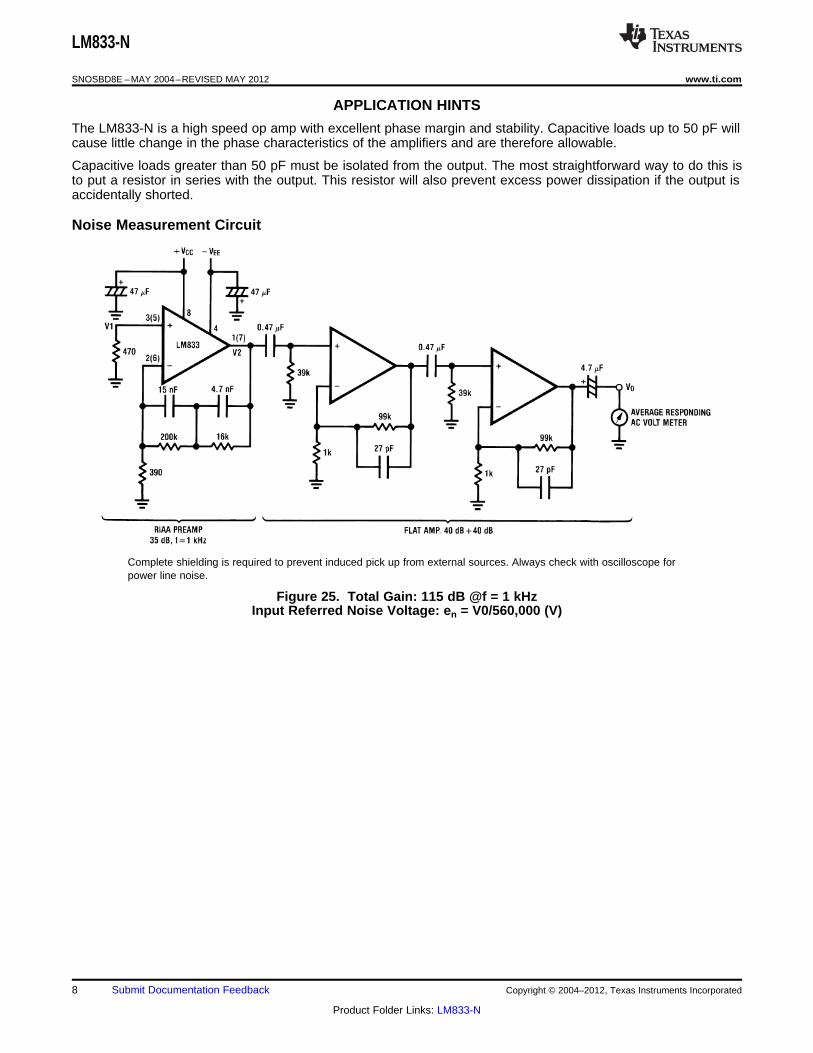
APPLICATION HINTS
The LM833-N is a high speed op amp with excellent phase margin and stability. Capacitive loads up to 50 pF willcause little change in the phase characteristics of the amplifiers and are therefore allowable.
Capacitive loads greater than 50 pF must be isolated from the output. The most straightforward way to do this isto put a resistor in series with the output. This resistor will also prevent excess power dissipation if the output isaccidentally shorted.
Noise Measurement Circuit
Complete shielding is required to prevent induced pick up from external sources. Always check with oscilloscope forpower line noise.
Figure 25. Total Gain: 115 dB @f = 1 kHzInput Referred Noise Voltage: en = V0/560,000 (V)
8 Submit Documentation Feedback Copyright © 2004–2012, Texas Instruments Incorporated
Product Folder Links: LM833-N
LM833-N
www.ti.com SNOSBD8E –MAY 2004–REVISED MAY 2012
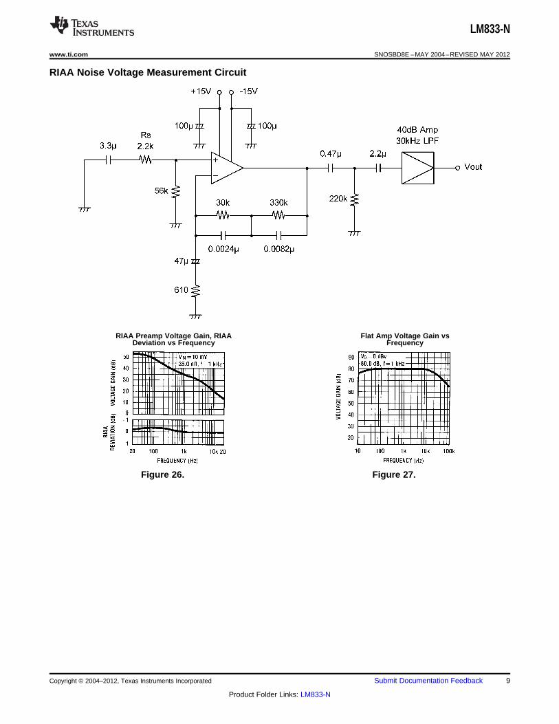
RIAA Noise Voltage Measurement Circuit
RIAA Preamp Voltage Gain, RIAA Flat Amp Voltage Gain vsDeviation vs Frequency Frequency
Figure 26. Figure 27.
Copyright © 2004–2012, Texas Instruments Incorporated Submit Documentation Feedback 9
Product Folder Links: LM833-N

LM833-N
SNOSBD8E –MAY 2004–REVISED MAY 2012 www.ti.com
Typical Applications
AV = 34.5F = 1 kHzEn = 0.38 μVA Weighted
Figure 28. NAB Preamp
Figure 29. NAB Preamp Voltage Gain vs Frequency
VO = V1–V2
Figure 30. Balanced to Single Ended Converter
10 Submit Documentation Feedback Copyright © 2004–2012, Texas Instruments Incorporated
Product Folder Links: LM833-N
LM833-N
www.ti.com SNOSBD8E –MAY 2004–REVISED MAY 2012
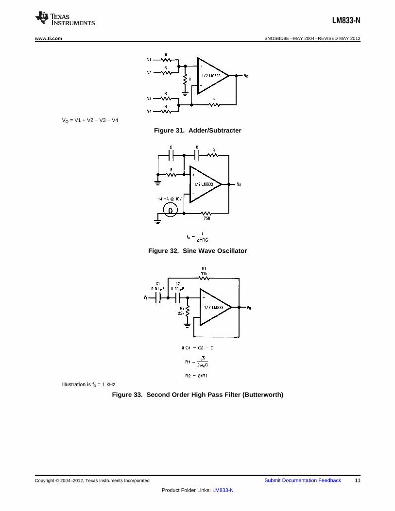
VO = V1 + V2 − V3 − V4
Figure 31. Adder/Subtracter
Figure 32. Sine Wave Oscillator
Illustration is f0 = 1 kHz
Figure 33. Second Order High Pass Filter (Butterworth)
Copyright © 2004–2012, Texas Instruments Incorporated Submit Documentation Feedback 11
Product Folder Links: LM833-N
LM833-N
SNOSBD8E –MAY 2004–REVISED MAY 2012 www.ti.com
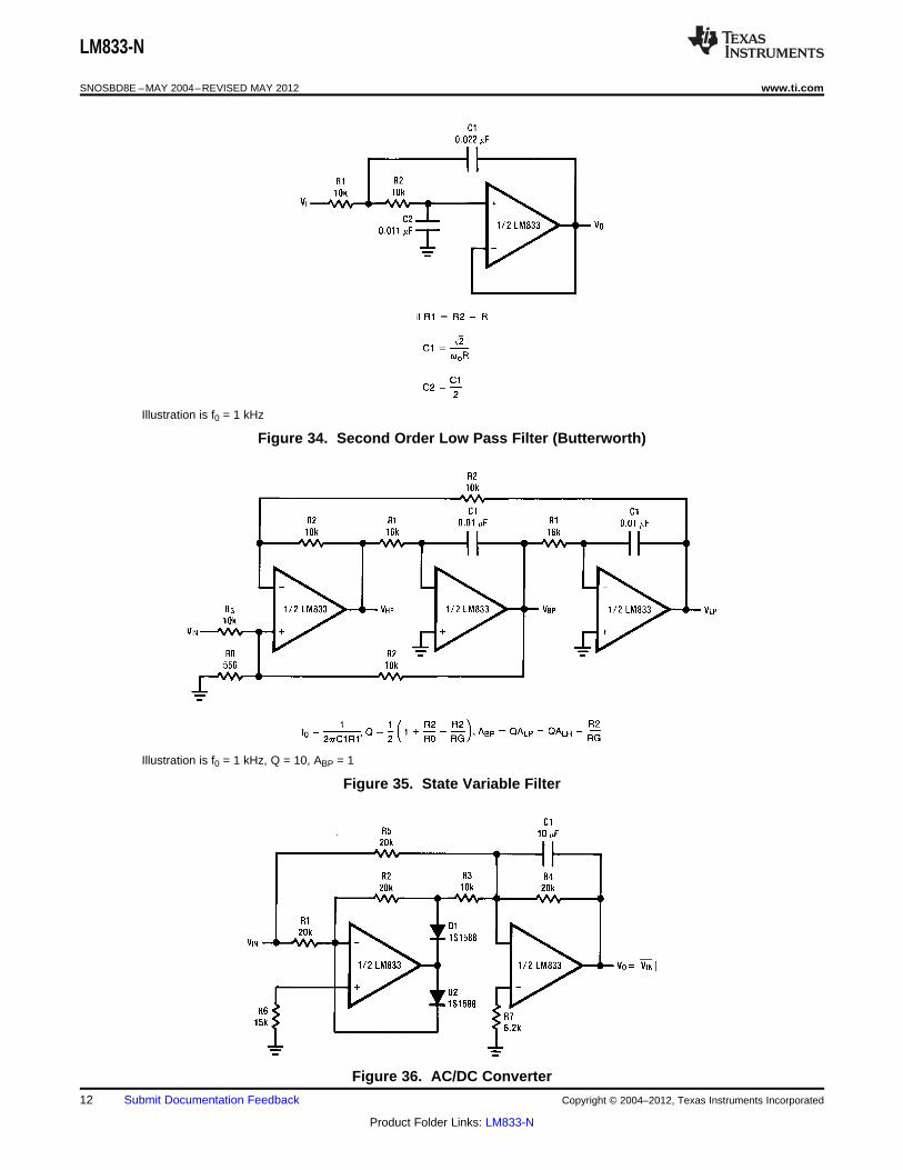
Illustration is f0 = 1 kHz
Figure 34. Second Order Low Pass Filter (Butterworth)
Illustration is f0 = 1 kHz, Q = 10, ABP = 1
Figure 35. State Variable Filter
Figure 36. AC/DC Converter
12 Submit Documentation Feedback Copyright © 2004–2012, Texas Instruments Incorporated
Product Folder Links: LM833-N
LM833-N
www.ti.com SNOSBD8E –MAY 2004–REVISED MAY 2012
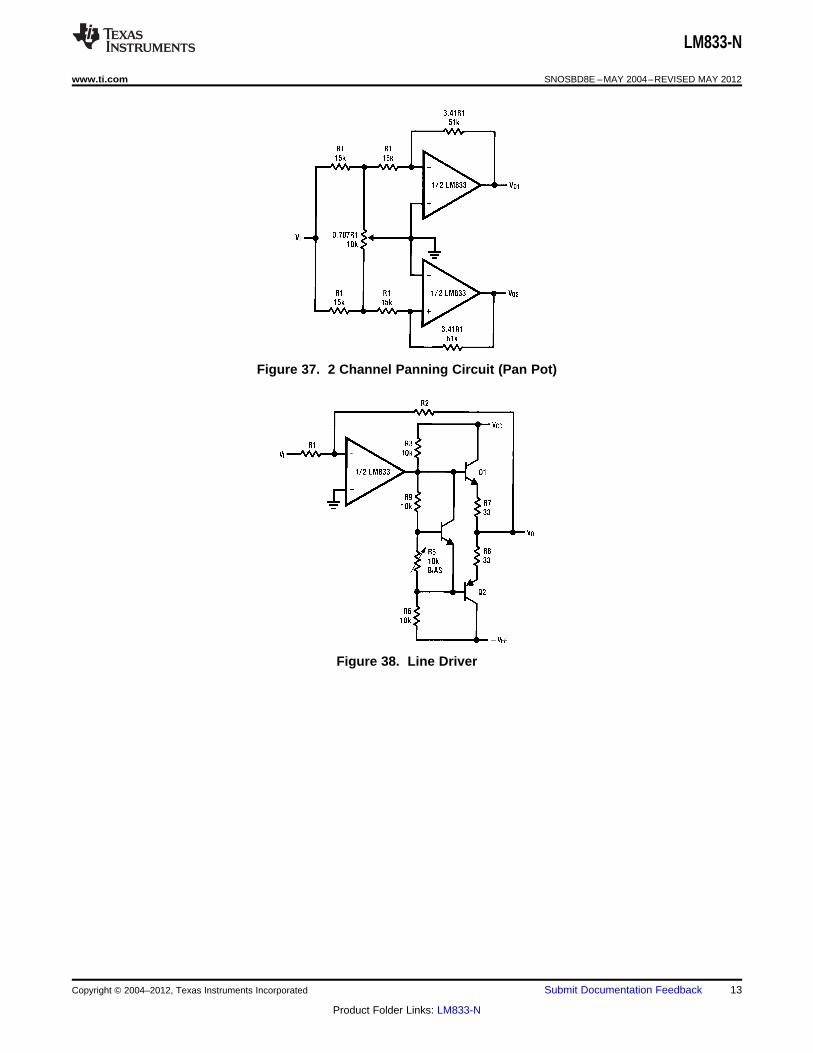
Figure 37. 2 Channel Panning Circuit (Pan Pot)
Figure 38. Line Driver
Copyright © 2004–2012, Texas Instruments Incorporated Submit Documentation Feedback 13
Product Folder Links: LM833-N
LM833-N
SNOSBD8E –MAY 2004–REVISED MAY 2012 www.ti.com
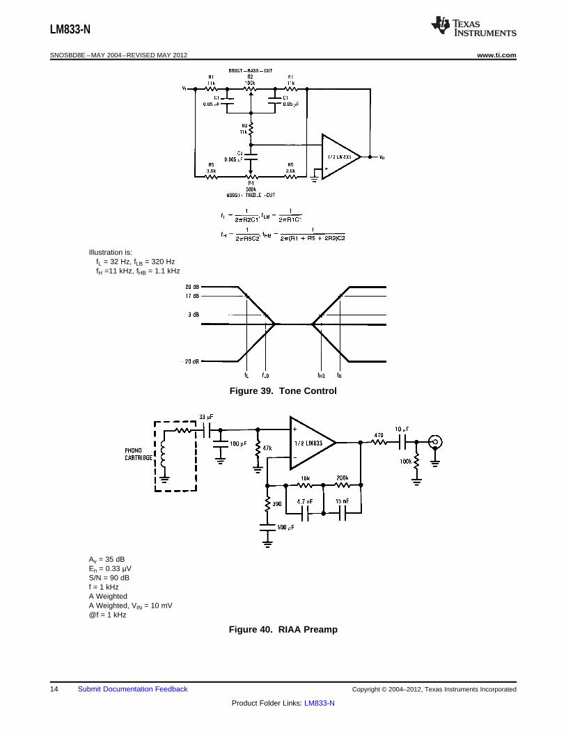
Illustration is:fL = 32 Hz, fLB = 320 HzfH =11 kHz, fHB = 1.1 kHz
Figure 39. Tone Control
Av = 35 dBEn = 0.33 μVS/N = 90 dBf = 1 kHzA WeightedA Weighted, VIN = 10 mV@f = 1 kHz
Figure 40. RIAA Preamp
14 Submit Documentation Feedback Copyright © 2004–2012, Texas Instruments Incorporated
Product Folder Links: LM833-N
LM833-N
www.ti.com SNOSBD8E –MAY 2004–REVISED MAY 2012
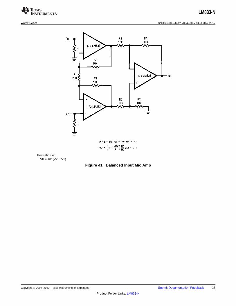
Illustration is:V0 = 101(V2 − V1)
Figure 41. Balanced Input Mic Amp
Copyright © 2004–2012, Texas Instruments Incorporated Submit Documentation Feedback 15
Product Folder Links: LM833-N
LM833-N
SNOSBD8E –MAY 2004–REVISED MAY 2012 www.ti.com
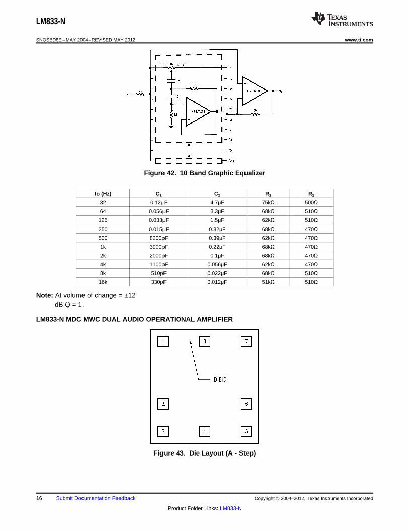
Figure 42. 10 Band Graphic Equalizer
fo (Hz) C1 C2 R1 R2
32 0.12μF 4.7μF 75kΩ 500Ω64 0.056μF 3.3μF 68kΩ 510Ω125 0.033μF 1.5μF 62kΩ 510Ω250 0.015μF 0.82μF 68kΩ 470Ω500 8200pF 0.39μF 62kΩ 470Ω1k 3900pF 0.22μF 68kΩ 470Ω2k 2000pF 0.1μF 68kΩ 470Ω4k 1100pF 0.056μF 62kΩ 470Ω8k 510pF 0.022μF 68kΩ 510Ω16k 330pF 0.012μF 51kΩ 510Ω
Note: At volume of change = ±12dB Q = 1.
LM833-N MDC MWC DUAL AUDIO OPERATIONAL AMPLIFIER
Figure 43. Die Layout (A - Step)
16 Submit Documentation Feedback Copyright © 2004–2012, Texas Instruments Incorporated
Product Folder Links: LM833-N
PACKAGE OPTION ADDENDUM
www.ti.com 18-Nov-2015
Addendum-Page 1
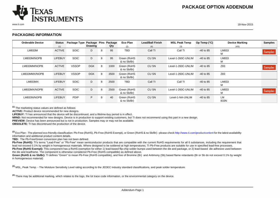
PACKAGING INFORMATION
Orderable Device Status(1)
Package Type PackageDrawing
Pins PackageQty
Eco Plan(2)
Lead/Ball Finish(6)
MSL Peak Temp(3)
Op Temp (°C) Device Marking(4/5)
Samples
LM833M ACTIVE SOIC D 8 95 TBD Call TI Call TI -40 to 85 LM833M
LM833M/NOPB LIFEBUY SOIC D 8 95 Green (RoHS& no Sb/Br)
CU SN Level-1-260C-UNLIM -40 to 85 LM833M
LM833MM/NOPB ACTIVE VSSOP DGK 8 1000 Green (RoHS& no Sb/Br)
CU SN Level-1-260C-UNLIM -40 to 85 Z83
LM833MMX/NOPB LIFEBUY VSSOP DGK 8 3500 Green (RoHS& no Sb/Br)
CU SN Level-1-260C-UNLIM -40 to 85 Z83
LM833MX LIFEBUY SOIC D 8 2500 TBD Call TI Call TI -40 to 85 LM833M
LM833MX/NOPB ACTIVE SOIC D 8 2500 Green (RoHS& no Sb/Br)
CU SN Level-1-260C-UNLIM -40 to 85 LM833M
LM833N/NOPB LIFEBUY PDIP P 8 40 Green (RoHS& no Sb/Br)
CU SN Level-1-NA-UNLIM -40 to 85 LM833N
(1) The marketing status values are defined as follows:ACTIVE: Product device recommended for new designs.LIFEBUY: TI has announced that the device will be discontinued, and a lifetime-buy period is in effect.NRND: Not recommended for new designs. Device is in production to support existing customers, but TI does not recommend using this part in a new design.PREVIEW: Device has been announced but is not in production. Samples may or may not be available.OBSOLETE: TI has discontinued the production of the device.
(2) Eco Plan - The planned eco-friendly classification: Pb-Free (RoHS), Pb-Free (RoHS Exempt), or Green (RoHS & no Sb/Br) - please check http://www.ti.com/productcontent for the latest availabilityinformation and additional product content details.TBD: The Pb-Free/Green conversion plan has not been defined.Pb-Free (RoHS): TI's terms "Lead-Free" or "Pb-Free" mean semiconductor products that are compatible with the current RoHS requirements for all 6 substances, including the requirement thatlead not exceed 0.1% by weight in homogeneous materials. Where designed to be soldered at high temperatures, TI Pb-Free products are suitable for use in specified lead-free processes.Pb-Free (RoHS Exempt): This component has a RoHS exemption for either 1) lead-based flip-chip solder bumps used between the die and package, or 2) lead-based die adhesive used betweenthe die and leadframe. The component is otherwise considered Pb-Free (RoHS compatible) as defined above.Green (RoHS & no Sb/Br): TI defines "Green" to mean Pb-Free (RoHS compatible), and free of Bromine (Br) and Antimony (Sb) based flame retardants (Br or Sb do not exceed 0.1% by weightin homogeneous material)
(3) MSL, Peak Temp. - The Moisture Sensitivity Level rating according to the JEDEC industry standard classifications, and peak solder temperature.
(4) There may be additional marking, which relates to the logo, the lot trace code information, or the environmental category on the device.
PACKAGE OPTION ADDENDUM
www.ti.com 18-Nov-2015
Addendum-Page 2
(5) Multiple Device Markings will be inside parentheses. Only one Device Marking contained in parentheses and separated by a "~" will appear on a device. If a line is indented then it is a continuationof the previous line and the two combined represent the entire Device Marking for that device.
(6) Lead/Ball Finish - Orderable Devices may have multiple material finish options. Finish options are separated by a vertical ruled line. Lead/Ball Finish values may wrap to two lines if the finishvalue exceeds the maximum column width.
Important Information and Disclaimer:The information provided on this page represents TI's knowledge and belief as of the date that it is provided. TI bases its knowledge and belief on informationprovided by third parties, and makes no representation or warranty as to the accuracy of such information. Efforts are underway to better integrate information from third parties. TI has taken andcontinues to take reasonable steps to provide representative and accurate information but may not have conducted destructive testing or chemical analysis on incoming materials and chemicals.TI and TI suppliers consider certain information to be proprietary, and thus CAS numbers and other limited information may not be available for release.
In no event shall TI's liability arising out of such information exceed the total purchase price of the TI part(s) at issue in this document sold by TI to Customer on an annual basis.
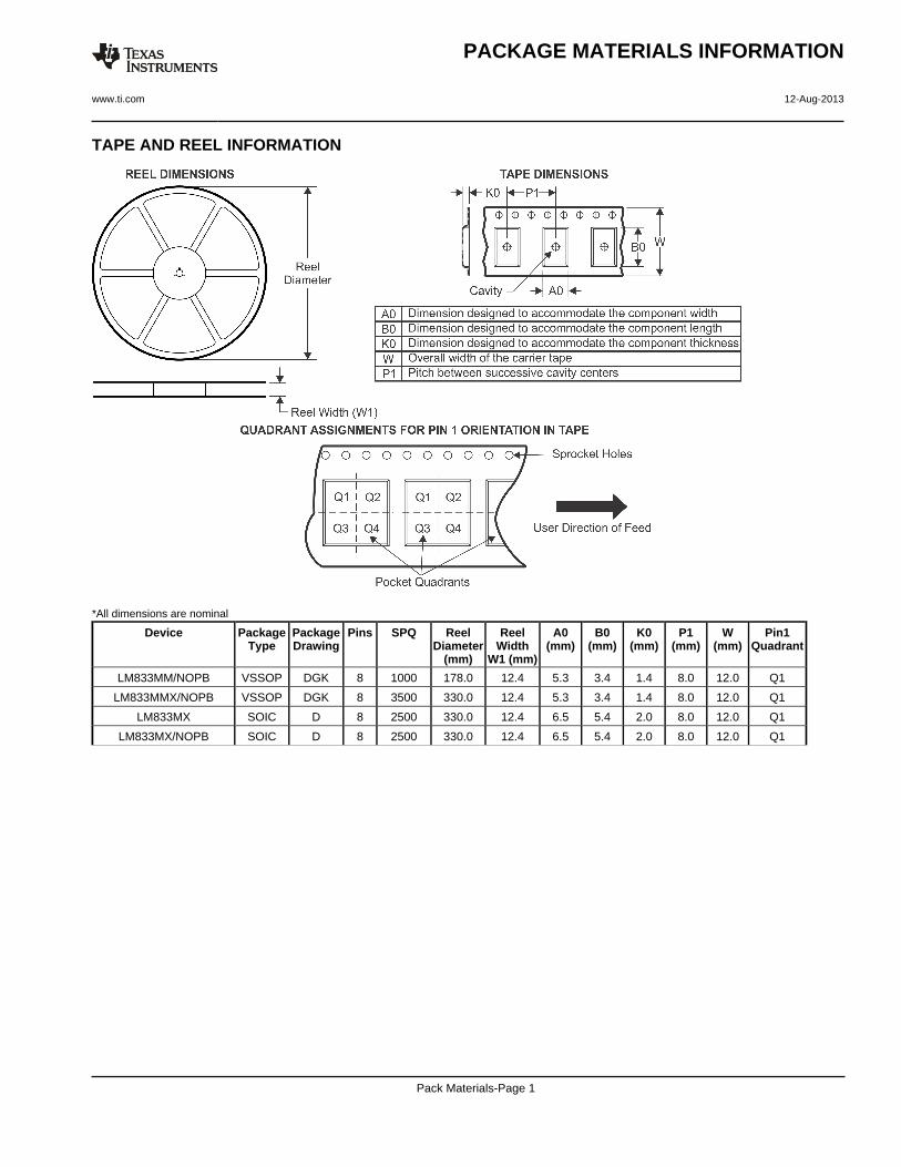
TAPE AND REEL INFORMATION
*All dimensions are nominal
Device PackageType
PackageDrawing
Pins SPQ ReelDiameter
(mm)
ReelWidth
W1 (mm)
A0(mm)
B0(mm)
K0(mm)
P1(mm)
W(mm)
Pin1Quadrant
LM833MM/NOPB VSSOP DGK 8 1000 178.0 12.4 5.3 3.4 1.4 8.0 12.0 Q1
LM833MMX/NOPB VSSOP DGK 8 3500 330.0 12.4 5.3 3.4 1.4 8.0 12.0 Q1
LM833MX SOIC D 8 2500 330.0 12.4 6.5 5.4 2.0 8.0 12.0 Q1
LM833MX/NOPB SOIC D 8 2500 330.0 12.4 6.5 5.4 2.0 8.0 12.0 Q1
PACKAGE MATERIALS INFORMATION
www.ti.com 12-Aug-2013
Pack Materials-Page 1
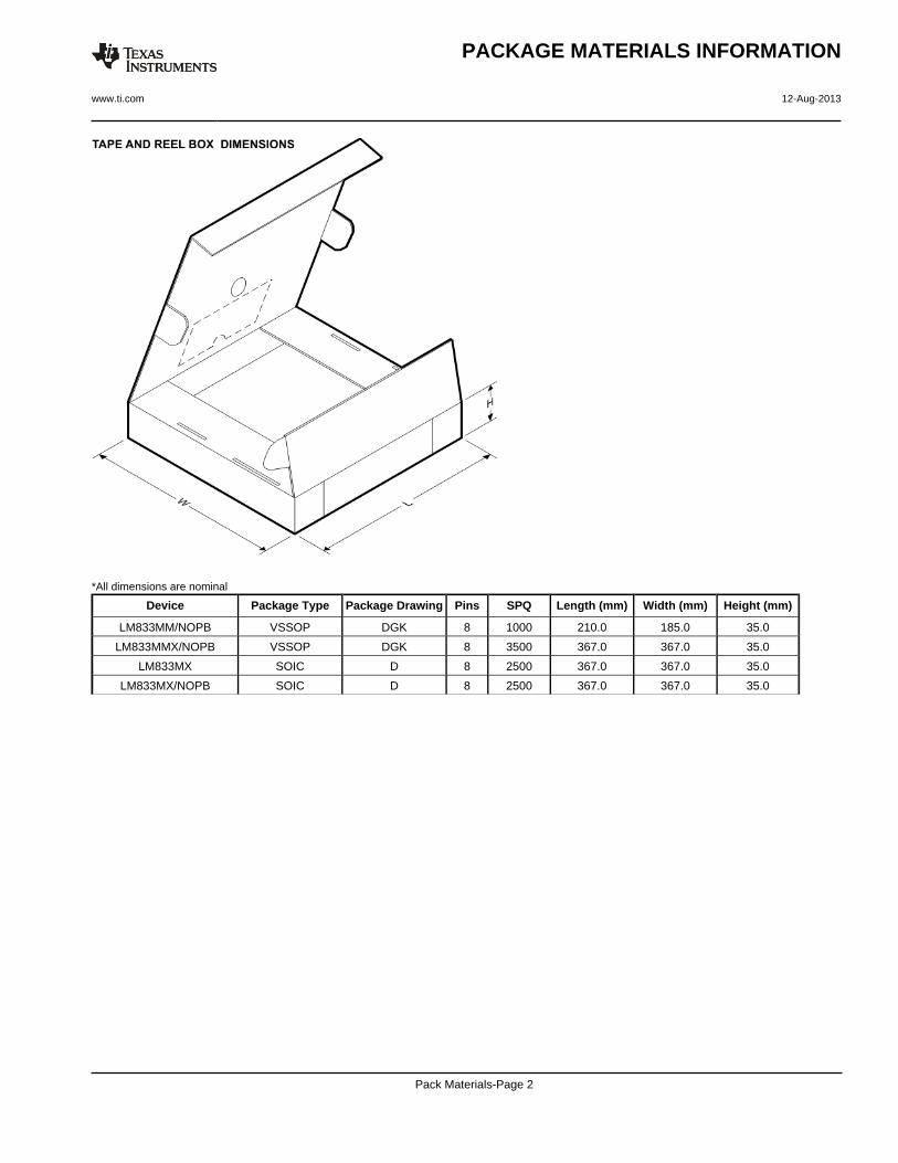
*All dimensions are nominal
Device Package Type Package Drawing Pins SPQ Length (mm) Width (mm) Height (mm)
LM833MM/NOPB VSSOP DGK 8 1000 210.0 185.0 35.0
LM833MMX/NOPB VSSOP DGK 8 3500 367.0 367.0 35.0
LM833MX SOIC D 8 2500 367.0 367.0 35.0
LM833MX/NOPB SOIC D 8 2500 367.0 367.0 35.0
PACKAGE MATERIALS INFORMATION
www.ti.com 12-Aug-2013
Pack Materials-Page 2
IMPORTANT NOTICE
Texas Instruments Incorporated and its subsidiaries (TI) reserve the right to make corrections, enhancements, improvements and otherchanges to its semiconductor products and services per JESD46, latest issue, and to discontinue any product or service per JESD48, latestissue. Buyers should obtain the latest relevant information before placing orders and should verify that such information is current andcomplete. All semiconductor products (also referred to herein as “components”) are sold subject to TI’s terms and conditions of salesupplied at the time of order acknowledgment.TI warrants performance of its components to the specifications applicable at the time of sale, in accordance with the warranty in TI’s termsand conditions of sale of semiconductor products. Testing and other quality control techniques are used to the extent TI deems necessaryto support this warranty. Except where mandated by applicable law, testing of all parameters of each component is not necessarilyperformed.TI assumes no liability for applications assistance or the design of Buyers’ products. Buyers are responsible for their products andapplications using TI components. To minimize the risks associated with Buyers’ products and applications, Buyers should provideadequate design and operating safeguards.TI does not warrant or represent that any license, either express or implied, is granted under any patent right, copyright, mask work right, orother intellectual property right relating to any combination, machine, or process in which TI components or services are used. Informationpublished by TI regarding third-party products or services does not constitute a license to use such products or services or a warranty orendorsement thereof. Use of such information may require a license from a third party under the patents or other intellectual property of thethird party, or a license from TI under the patents or other intellectual property of TI.Reproduction of significant portions of TI information in TI data books or data sheets is permissible only if reproduction is without alterationand is accompanied by all associated warranties, conditions, limitations, and notices. TI is not responsible or liable for such altereddocumentation. Information of third parties may be subject to additional restrictions.Resale of TI components or services with statements different from or beyond the parameters stated by TI for that component or servicevoids all express and any implied warranties for the associated TI component or service and is an unfair and deceptive business practice.TI is not responsible or liable for any such statements.Buyer acknowledges and agrees that it is solely responsible for compliance with all legal, regulatory and safety-related requirementsconcerning its products, and any use of TI components in its applications, notwithstanding any applications-related information or supportthat may be provided by TI. Buyer represents and agrees that it has all the necessary expertise to create and implement safeguards whichanticipate dangerous consequences of failures, monitor failures and their consequences, lessen the likelihood of failures that might causeharm and take appropriate remedial actions. Buyer will fully indemnify TI and its representatives against any damages arising out of the useof any TI components in safety-critical applications.In some cases, TI components may be promoted specifically to facilitate safety-related applications. With such components, TI’s goal is tohelp enable customers to design and create their own end-product solutions that meet applicable functional safety standards andrequirements. Nonetheless, such components are subject to these terms.No TI components are authorized for use in FDA Class III (or similar life-critical medical equipment) unless authorized officers of the partieshave executed a special agreement specifically governing such use.Only those TI components which TI has specifically designated as military grade or “enhanced plastic” are designed and intended for use inmilitary/aerospace applications or environments. Buyer acknowledges and agrees that any military or aerospace use of TI componentswhich have not been so designated is solely at the Buyer's risk, and that Buyer is solely responsible for compliance with all legal andregulatory requirements in connection with such use.TI has specifically designated certain components as meeting ISO/TS16949 requirements, mainly for automotive use. In any case of use ofnon-designated products, TI will not be responsible for any failure to meet ISO/TS16949.
Products ApplicationsAudio www.ti.com/audio Automotive and Transportation www.ti.com/automotiveAmplifiers amplifier.ti.com Communications and Telecom www.ti.com/communicationsData Converters dataconverter.ti.com Computers and Peripherals www.ti.com/computersDLP® Products www.dlp.com Consumer Electronics www.ti.com/consumer-appsDSP dsp.ti.com Energy and Lighting www.ti.com/energyClocks and Timers www.ti.com/clocks Industrial www.ti.com/industrialInterface interface.ti.com Medical www.ti.com/medicalLogic logic.ti.com Security www.ti.com/securityPower Mgmt power.ti.com Space, Avionics and Defense www.ti.com/space-avionics-defenseMicrocontrollers microcontroller.ti.com Video and Imaging www.ti.com/videoRFID www.ti-rfid.comOMAP Applications Processors www.ti.com/omap TI E2E Community e2e.ti.comWireless Connectivity www.ti.com/wirelessconnectivity
Mailing Address: Texas Instruments, Post Office Box 655303, Dallas, Texas 75265Copyright © 2015, Texas Instruments Incorporated