8 bit PIPO shift register with asynchronous clear Sheets/ST...8 BIT PIPO SHIFT REGISTER WITH...
13
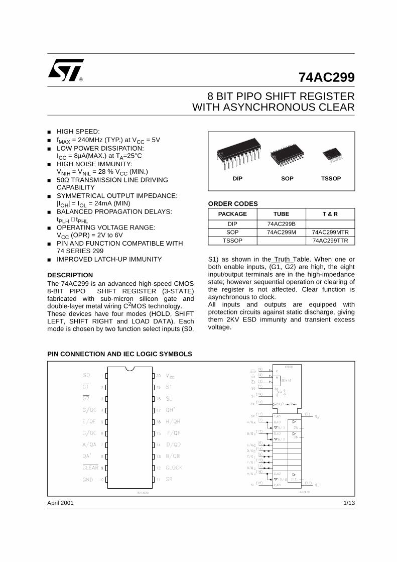
1/13 April 2001 ■ HIGH SPEED: ■ f MAX = 240MHz (TYP.) at V CC = 5V ■ LOW POWER DISSIPATION: I CC = 8μA(MAX.) at T A =25°C ■ HIGH NOISE IMMUNITY: V NIH = V NIL = 28 % V CC (MIN.) ■ 50Ω TRANSMISSION LINE DRIVING CAPABILITY ■ SYMMETRICAL OUTPUT IMPEDANCE: |I OH | = I OL = 24mA (MIN) ■ BALANCED PROPAGATION DELAYS: t PLH 2245 t PHL ■ OPERATING VOLTAGE RANGE: V CC (OPR) = 2V to 6V ■ PIN AND FUNCTION COMPATIBLE WITH 74 SERIES 299 ■ IMPROVED LATCH-UP IMMUNITY DESCRIPTION The 74AC299 is an advanced high-speed CMOS 8-BIT PIPO SHIFT REGISTER (3-STATE) fabricated with sub-micron silicon gate and double-layer metal wiring C 2 MOS technology. These devices have four modes (HOLD, SHIFT LEFT, SHIFT RIGHT and LOAD DATA). Each mode is chosen by two function select inputs (S0, S1) as shown in the Truth Table. When one or both enable inputs, (G1 , G2 ) are high, the eight input/output terminals are in the high-impedance state; however sequential operation or clearing of the register is not affected. Clear function is asynchronous to clock. All inputs and outputs are equipped with protection circuits against static discharge, giving them 2KV ESD immunity and transient excess voltage. 74AC299 8 BIT PIPO SHIFT REGISTER WITH ASYNCHRONOUS CLEAR PIN CONNECTION AND IEC LOGIC SYMBOLS ORDER CODES PACKAGE TUBE T & R DIP 74AC299B SOP 74AC299M 74AC299MTR TSSOP 74AC299TTR TSSOP DIP SOP
Transcript of 8 bit PIPO shift register with asynchronous clear Sheets/ST...8 BIT PIPO SHIFT REGISTER WITH...
1/13April 2001
HIGH SPEED: fMAX = 240MHz (TYP.) at VCC = 5V LOW POWER DISSIPATION:
ICC = 8µA(MAX.) at TA=25°C HIGH NOISE IMMUNITY:
VNIH = VNIL = 28 % VCC (MIN.) 50Ω TRANSMISSION LINE DRIVING
CAPABILITY SYMMETRICAL OUTPUT IMPEDANCE:
|IOH| = IOL = 24mA (MIN) BALANCED PROPAGATION DELAYS:
tPLH ≅ tPHL OPERATING VOLTAGE RANGE:
VCC (OPR) = 2V to 6V PIN AND FUNCTION COMPATIBLE WITH
74 SERIES 299 IMPROVED LATCH-UP IMMUNITY
DESCRIPTIONThe 74AC299 is an advanced high-speed CMOS8-BIT PIPO SHIFT REGISTER (3-STATE)fabricated with sub-micron silicon gate anddouble-layer metal wiring C2MOS technology. These devices have four modes (HOLD, SHIFTLEFT, SHIFT RIGHT and LOAD DATA). Eachmode is chosen by two function select inputs (S0,
S1) as shown in the Truth Table. When one orboth enable inputs, (G1, G2) are high, the eightinput/output terminals are in the high-impedancestate; however sequential operation or clearing ofthe register is not affected. Clear function isasynchronous to clock.All inputs and outputs are equipped withprotection circuits against static discharge, givingthem 2KV ESD immunity and transient excessvoltage.
74AC2998 BIT PIPO SHIFT REGISTER
WITH ASYNCHRONOUS CLEAR
PIN CONNECTION AND IEC LOGIC SYMBOLS
ORDER CODES
PACKAGE TUBE T & R
DIP 74AC299B
SOP 74AC299M 74AC299MTR
TSSOP 74AC299TTR
TSSOPDIP SOP
74AC299
2/13
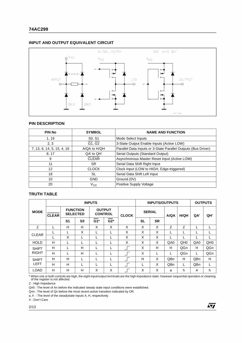
INPUT AND OUTPUT EQUIVALENT CIRCUIT
PIN DESCRIPTION
TRUTH TABLE
* When one or both controls are high, the eight input/output terminals are the high impedance state: howewer sequential operation or cleaning of the register is not affected.
Z : High ImpedanceQn0 : The level of An before the indicated steady state input conditions were established.Qnn : The level of Qn before the most recent active transition indicated by ORa, h : The level of the steadystate inputs A, H, respectively.X : Don’t Care
PIN No SYMBOL NAME AND FUNCTION
1, 19 S0, S1 Mode Select Inputs
2, 3 G1, G2 3-State Output Enable Inputs (Active LOW)
7, 13, 6, 14, 5, 15, 4, 16 A/QA to H/QH Parallel Data Inputs or 3-State Parallel Outputs (Bus Driver)
8, 17 QA’ to QH’ Serial Outputs (Standard Output)
9 CLEAR Asynchronous Master Reset Input (Active LOW)
11 SR Serial Data Shift Right Input
12 CLOCK Clock Input (LOW to HIGH, Edge-triggered)
18 SL Serial Data Shift Left Input
10 GND Ground (0V)
20 VCC Positive Supply Voltage
MODE
INPUTS INPUTS/OUTPUTS OUTPUTS
CLEAR
FUNCTION SELECTED
OUTPUT CONTROL CLOCK
SERIALA/QA H/QH QA’ QH’
S1 S0 G1* G2* SL SR
Z L H H X X X X X Z Z L L
CLEARL L X L L X X X L L L L
L X L L L X X X L L L L
HOLD H L L L L X X X QA0 QH0 QA0 QH0
SHIFT RIGHT
H L H L L X H H QGn H QGn
H L H L L X L L QGn L QGn
SHIFT LEFT
H H L L L H X QBn H QBn H
H H L L L L X QBn L QBn L
LOAD H H H X X X X a h a h
74AC299
3/13
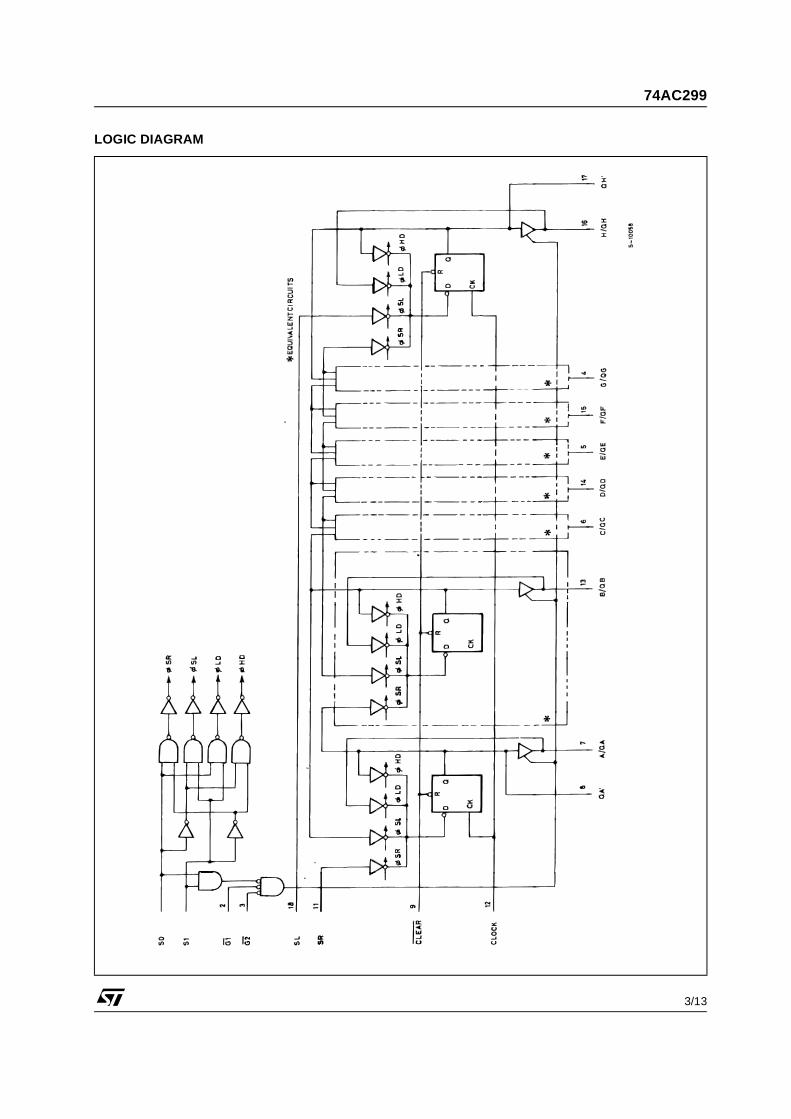
LOGIC DIAGRAM
74AC299
4/13
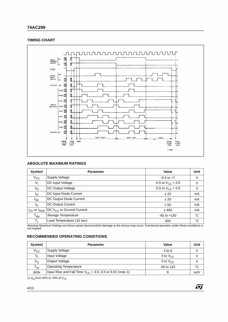
TIMING CHART
ABSOLUTE MAXIMUM RATINGS
Absolute Maximum Ratings are those values beyond which damage to the device may occur. Functional operation under these conditions is not implied.
RECOMMENDED OPERATING CONDITIONS
1) VIN from 30% to 70% of VCC
Symbol Parameter Value Unit
VCC Supply Voltage -0.5 to +7 V
VI DC Input Voltage -0.5 to VCC + 0.5 V
VO DC Output Voltage -0.5 to VCC + 0.5 V
IIK DC Input Diode Current ± 20 mA
IOK DC Output Diode Current ± 20 mA
IO DC Output Current ± 50 mA
ICC or IGND DC VCC or Ground Current ± 400 mA
Tstg Storage Temperature -65 to +150 °C
TL Lead Temperature (10 sec) 300 °C
Symbol Parameter Value Unit
VCC Supply Voltage 2 to 6 V
VI Input Voltage 0 to VCC V
VO Output Voltage 0 to VCC V
Top Operating Temperature -55 to 125 °C
dt/dv Input Rise and Fall Time VCC = 3.0, 4.5 or 5.5V (note 1) 8 ns/V
74AC299
5/13
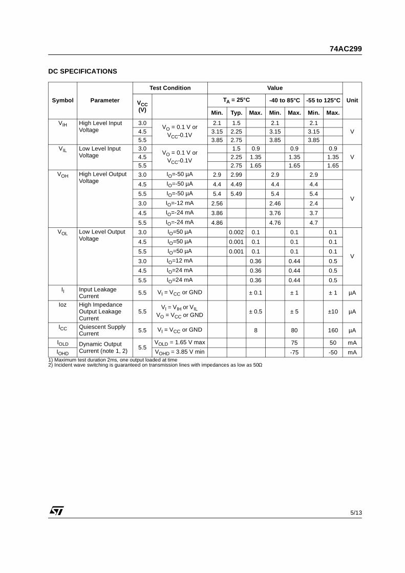
DC SPECIFICATIONS
1) Maximum test duration 2ms, one output loaded at time2) Incident wave switching is guaranteed on transmission lines with impedances as low as 50Ω
Symbol Parameter
Test Condition Value
UnitVCC(V)
TA = 25°C -40 to 85°C -55 to 125°C
Min. Typ. Max. Min. Max. Min. Max.
VIH High Level Input Voltage
3.0VO = 0.1 V or
VCC-0.1V
2.1 1.5 2.1 2.1
V4.5 3.15 2.25 3.15 3.15
5.5 3.85 2.75 3.85 3.85
VIL Low Level Input Voltage
3.0VO = 0.1 V or
VCC-0.1V
1.5 0.9 0.9 0.9
V4.5 2.25 1.35 1.35 1.35
5.5 2.75 1.65 1.65 1.65
VOH High Level Output Voltage
3.0 IO=-50 µA 2.9 2.99 2.9 2.9
V
4.5 IO=-50 µA 4.4 4.49 4.4 4.4
5.5 IO=-50 µA 5.4 5.49 5.4 5.4
3.0 IO=-12 mA 2.56 2.46 2.4
4.5 IO=-24 mA 3.86 3.76 3.7
5.5 IO=-24 mA 4.86 4.76 4.7
VOL Low Level Output Voltage
3.0 IO=50 µA 0.002 0.1 0.1 0.1
V
4.5 IO=50 µA 0.001 0.1 0.1 0.1
5.5 IO=50 µA 0.001 0.1 0.1 0.1
3.0 IO=12 mA 0.36 0.44 0.5
4.5 IO=24 mA 0.36 0.44 0.5
5.5 IO=24 mA 0.36 0.44 0.5
II Input Leakage Current
5.5 VI = VCC or GND ± 0.1 ± 1 ± 1 µA
Ioz High Impedance Output Leakage Current
5.5VI = VIH or VIL
VO = VCC or GND± 0.5 ± 5 ±10 µA
ICC Quiescent Supply Current 5.5 VI = VCC or GND 8 80 160 µA
IOLD Dynamic Output Current (note 1, 2)
5.5VOLD = 1.65 V max 75 50 mA
IOHD VOHD = 3.85 V min -75 -50 mA
74AC299
6/13
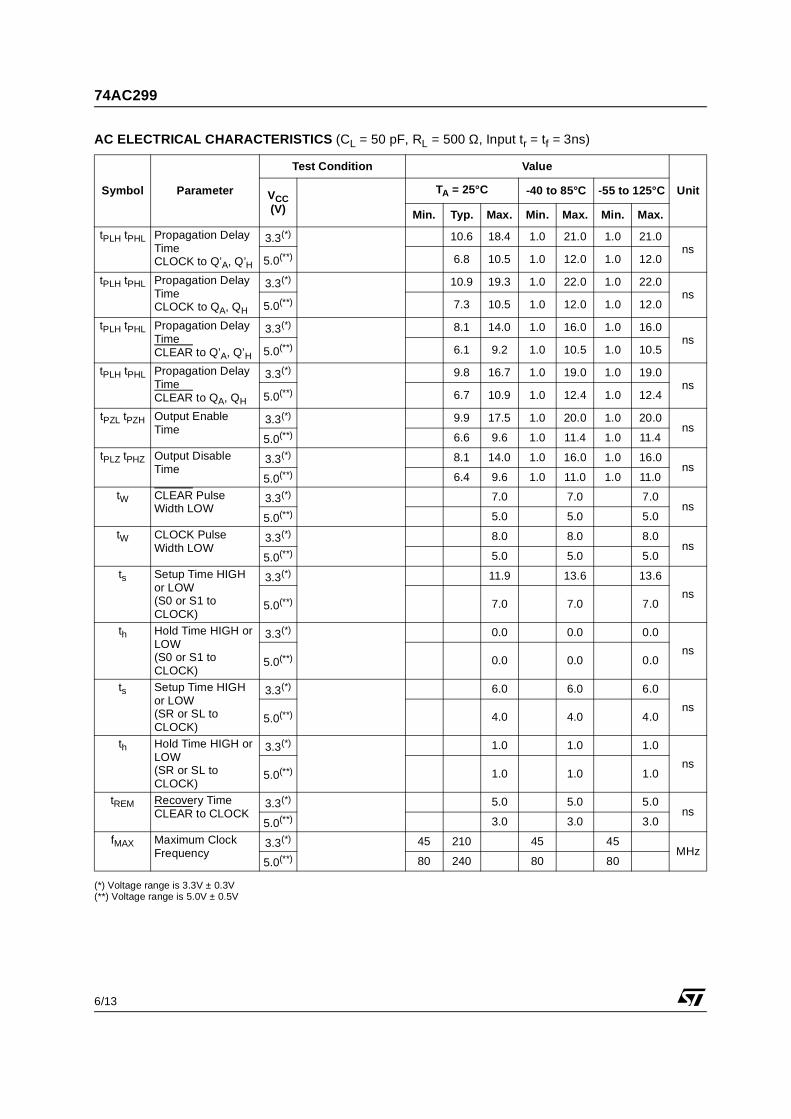
AC ELECTRICAL CHARACTERISTICS (CL = 50 pF, RL = 500 Ω, Input tr = tf = 3ns)
(*) Voltage range is 3.3V ± 0.3V(**) Voltage range is 5.0V ± 0.5V
Symbol Parameter
Test Condition Value
UnitVCC(V)
TA = 25°C -40 to 85°C -55 to 125°C
Min. Typ. Max. Min. Max. Min. Max.
tPLH tPHL Propagation Delay TimeCLOCK to Q’A, Q’H
3.3(*) 10.6 18.4 1.0 21.0 1.0 21.0ns
5.0(**) 6.8 10.5 1.0 12.0 1.0 12.0
tPLH tPHL Propagation Delay TimeCLOCK to QA, QH
3.3(*) 10.9 19.3 1.0 22.0 1.0 22.0ns
5.0(**) 7.3 10.5 1.0 12.0 1.0 12.0
tPLH tPHL Propagation Delay TimeCLEAR to Q’A, Q’H
3.3(*) 8.1 14.0 1.0 16.0 1.0 16.0ns
5.0(**) 6.1 9.2 1.0 10.5 1.0 10.5
tPLH tPHL Propagation Delay TimeCLEAR to QA, QH
3.3(*) 9.8 16.7 1.0 19.0 1.0 19.0ns
5.0(**) 6.7 10.9 1.0 12.4 1.0 12.4
tPZL tPZH Output Enable Time
3.3(*) 9.9 17.5 1.0 20.0 1.0 20.0ns
5.0(**) 6.6 9.6 1.0 11.4 1.0 11.4
tPLZ tPHZ Output Disable Time
3.3(*) 8.1 14.0 1.0 16.0 1.0 16.0ns
5.0(**) 6.4 9.6 1.0 11.0 1.0 11.0
tW CLEAR Pulse Width LOW
3.3(*) 7.0 7.0 7.0ns
5.0(**) 5.0 5.0 5.0
tW CLOCK Pulse Width LOW
3.3(*) 8.0 8.0 8.0ns
5.0(**) 5.0 5.0 5.0
ts Setup Time HIGH or LOW(S0 or S1 to CLOCK)
3.3(*) 11.9 13.6 13.6
ns5.0(**) 7.0 7.0 7.0
th Hold Time HIGH or LOW(S0 or S1 to CLOCK)
3.3(*) 0.0 0.0 0.0
ns5.0(**) 0.0 0.0 0.0
ts Setup Time HIGH or LOW(SR or SL to CLOCK)
3.3(*) 6.0 6.0 6.0
ns5.0(**) 4.0 4.0 4.0
th Hold Time HIGH or LOW(SR or SL to CLOCK)
3.3(*) 1.0 1.0 1.0
ns5.0(**) 1.0 1.0 1.0
tREM Recovery Time CLEAR to CLOCK
3.3(*) 5.0 5.0 5.0ns
5.0(**) 3.0 3.0 3.0
fMAX Maximum Clock Frequency
3.3(*) 45 210 45 45MHz
5.0(**) 80 240 80 80
74AC299
7/13
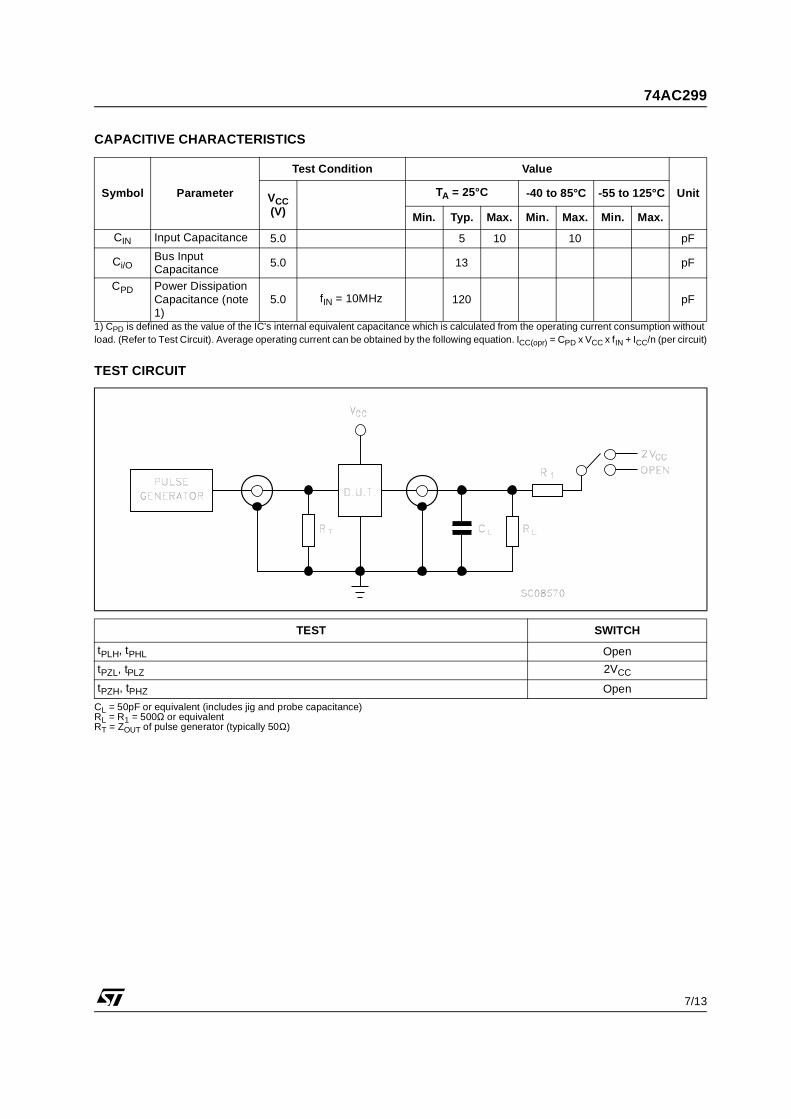
CAPACITIVE CHARACTERISTICS
1) CPD is defined as the value of the IC’s internal equivalent capacitance which is calculated from the operating current consumption without load. (Refer to Test Circuit). Average operating current can be obtained by the following equation. ICC(opr) = CPD x VCC x fIN + ICC/n (per circuit)
TEST CIRCUIT
CL = 50pF or equivalent (includes jig and probe capacitance)RL = R1 = 500Ω or equivalentRT = ZOUT of pulse generator (typically 50Ω)
Symbol Parameter
Test Condition Value
UnitVCC(V)
TA = 25°C -40 to 85°C -55 to 125°C
Min. Typ. Max. Min. Max. Min. Max.
CIN Input Capacitance 5.0 5 10 10 pF
Ci/OBus Input Capacitance
5.0 13 pF
CPD Power Dissipation Capacitance (note 1)
5.0 fIN = 10MHz 120 pF
TEST SWITCH
tPLH, tPHL Open
tPZL, tPLZ 2VCC
tPZH, tPHZ Open
74AC299
8/13
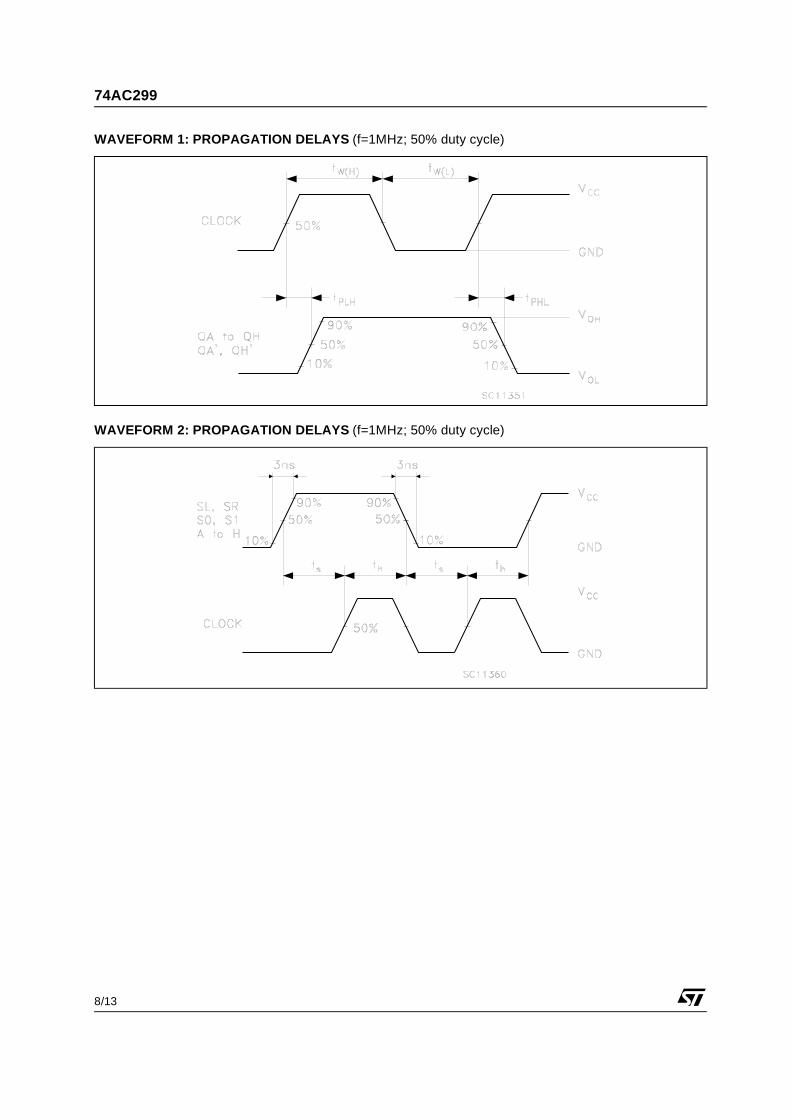
WAVEFORM 1: PROPAGATION DELAYS (f=1MHz; 50% duty cycle)
WAVEFORM 2: PROPAGATION DELAYS (f=1MHz; 50% duty cycle)
74AC299
9/13
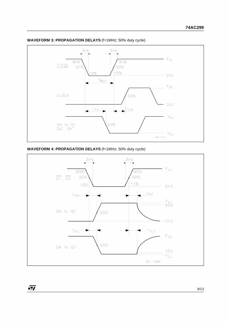
WAVEFORM 3: PROPAGATION DELAYS (f=1MHz; 50% duty cycle)
WAVEFORM 4: PROPAGATION DELAYS (f=1MHz; 50% duty cycle)
74AC299
10/13
DIM.mm inch
MIN. TYP. MAX. MIN. TYP. MAX.
a1 0.254 0.010
B 1.39 1.65 0.055 0.065
b 0.45 0.018
b1 0.25 0.010
D 25.4 1.000
E 8.5 0.335
e 2.54 0.100
e3 22.86 0.900
F 7.1 0.280
I 3.93 0.155
L 3.3 0.130
Z 1.34 0.053
P001J
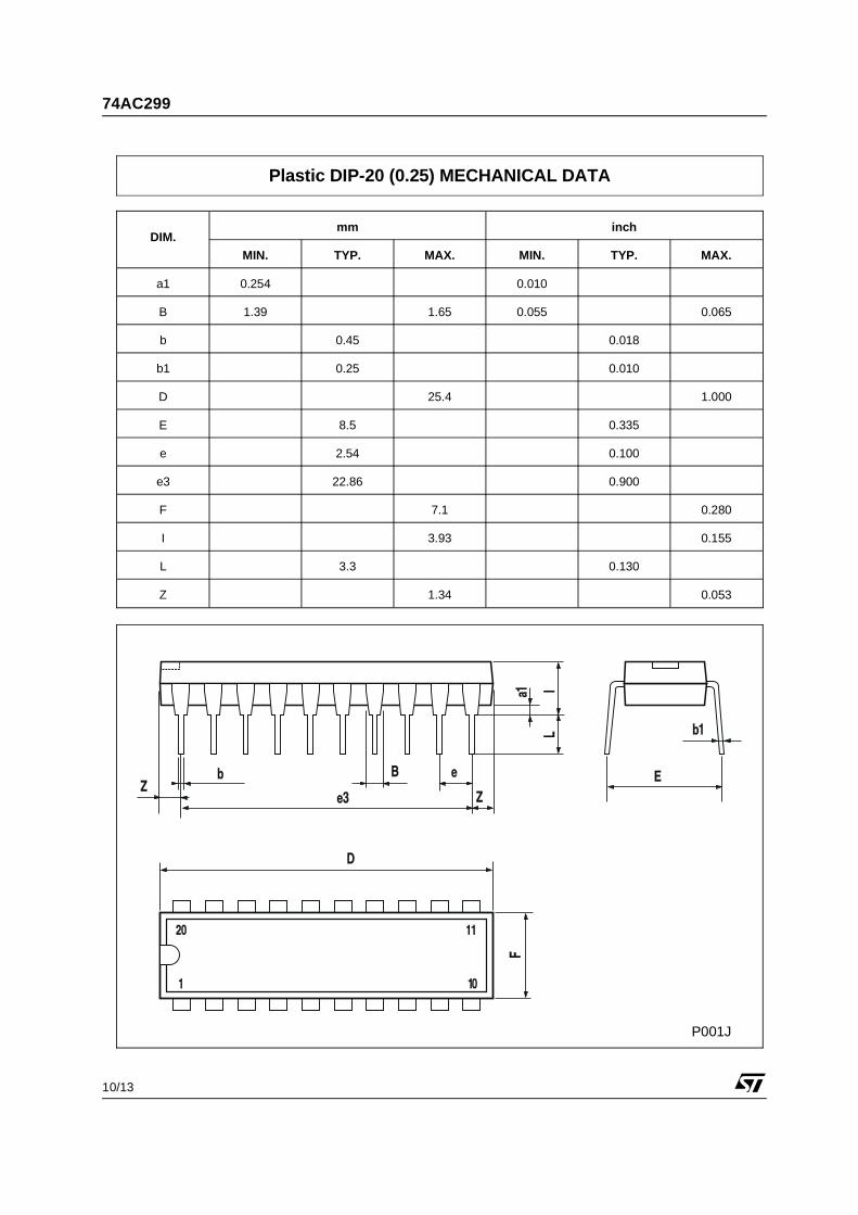
Plastic DIP-20 (0.25) MECHANICAL DATA
74AC299
11/13
DIM.mm inch
MIN. TYP. MAX. MIN. TYP. MAX.
A 2.65 0.104
a1 0.10 0.20 0.004 0.007
a2 2.45 0.096
b 0.35 0.49 0.013 0.019
b1 0.23 0.32 0.009 0.012
C 0.50 0.020
c1 45 (typ.)
D 12.60 13.00 0.496 0.512
E 10.00 10.65 0.393 0.419
e 1.27 0.050
e3 11.43 0.450
F 7.40 7.60 0.291 0.299
L 0.50 1.27 0.19 0.050
M 0.75 0.029
S 8 (max.)
P013L
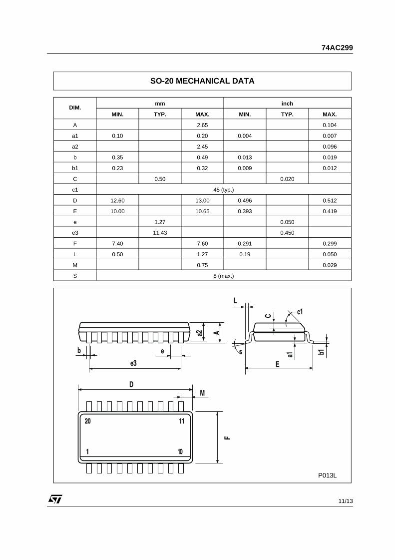
SO-20 MECHANICAL DATA
74AC299
12/13
DIM.mm inch
MIN. TYP. MAX. MIN. TYP. MAX.
A 1.1 0.433
A1 0.05 0.10 0.15 0.002 0.004 0.006
A2 0.85 0.9 0.95 0.335 0.354 0.374
b 0.19 0.30 0.0075 0.0118
c 0.09 0.2 0.0035 0.0079
D 6.4 6.5 6.6 0.252 0.256 0.260
E 6.25 6.4 6.5 0.246 0.252 0.256
E1 4.3 4.4 4.48 0.169 0.173 0.176
e 0.65 BSC 0.0256 BSC
K 0o 4o 8o 0o 4o 8o
L 0.50 0.60 0.70 0.020 0.024 0.028
c Eb
A2A
E1
D
1PIN 1 IDENTIFICATION
A1LK
e
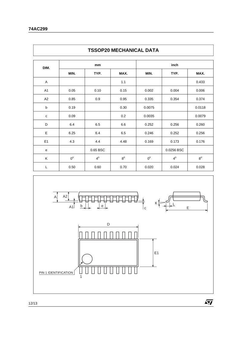
TSSOP20 MECHANICAL DATA
74AC299
Information furnished is believed to be accurate and reliable. However, STMicroelectronics assumes no responsibility for theconsequences of use of such information nor for any infringement of patents or other rights of third parties which may result fromits use. No license is granted by implication or otherwise under any patent or patent rights of STMicroelectronics. Specificationsmentioned in this publication are subject to change without notice. This publication supersedes and replaces all informationpreviously supplied. STMicroelectronics products are not authorized for use as critical components in life support devices orsystems without express written approval of STMicroelectronics.
© The ST logo is a registered trademark of STMicroelectronics
© 2001 STMicroelectronics - Printed in Italy - All Rights ReservedSTMicroelectronics GROUP OF COMPANIES
Australia - Brazil - China - Finland - France - Germany - Hong Kong - India - Italy - Japan - Malaysia - Malta - Morocco Singapore - Spain - Sweden - Switzerland - United Kingdom
© http://www.st.com
13/13


![arXiv:1605.09721v1 [stat.ML] 31 May 2016...CYCLADES: Conflict-free Asynchronous Machine Learning Xinghao Pan ; , Maximilian Lam , Stephen Tu ; Dimitris Papailiopoulos ; , Ce Zhangs](https://static.fdocument.org/doc/165x107/5f8d899fb11f266f02536443/arxiv160509721v1-statml-31-may-2016-cyclades-coniict-free-asynchronous.jpg)