The Avalanche Breakdown Voltage of PIN Diode
19
The Avalanche Breakdown Voltage of PIN Diode By Pathompron Jaikwang SCPY/B 6105012 Department of Physics, Faculty of Science, Mahidol University Email : [email protected] 1
Transcript of The Avalanche Breakdown Voltage of PIN Diode
The Avalanche Breakdown Voltage of PIN DiodeBy
Pathompron Jaikwang SCPY/B 6105012
Department of Physics, Faculty of Science, Mahidol University
Email : [email protected]
1
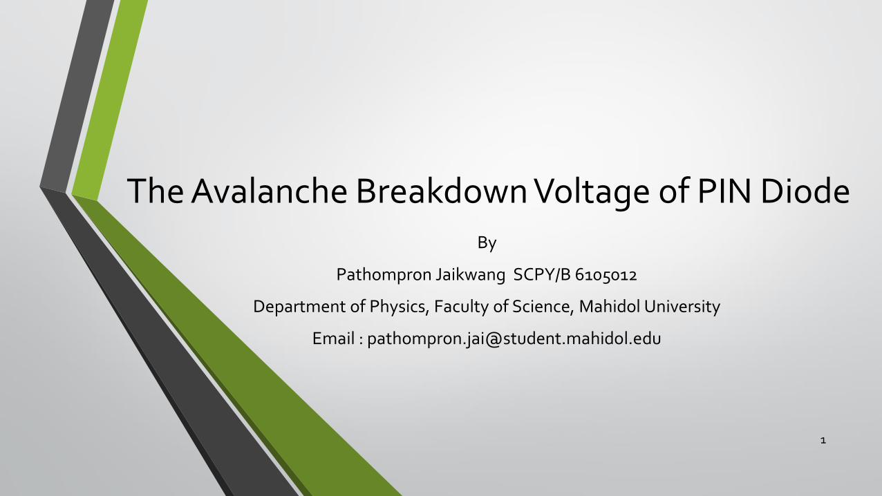
The Avalanche Diode
2
PIN Diode Chip Structure
https://www.microsemi.com/sites/default/files/datasheets/Products/rf/APPENDIX%20F.pdf
The application of PIN diodes as radiation detectors in particle counting, X‐ and γ‐ray spectroscopy, medical applications and charged particle spectroscopy is presented.
. The developed models have been used to study the impact of doping concentration on the breakdown voltage
Higher breakdown voltage is the primary requirement for a detectors.
Outline
• Introduction
• Basic Configuration of PN diode
• Band Diagram for a Reverse Bias Photodiode
• Basic Configuration of PIN Diode
• The Avalanche Breakdown Voltage
• Experiment
• The structure of PIN device
• Breakdown Voltage Characteristic Equation
• Result :The Avalanche BV Characteristic
• Conclusion3
Introduction The Avalanche Breakdown Voltage Experiment Conclusion
Basic Configuration of PN diode
PN diode
4
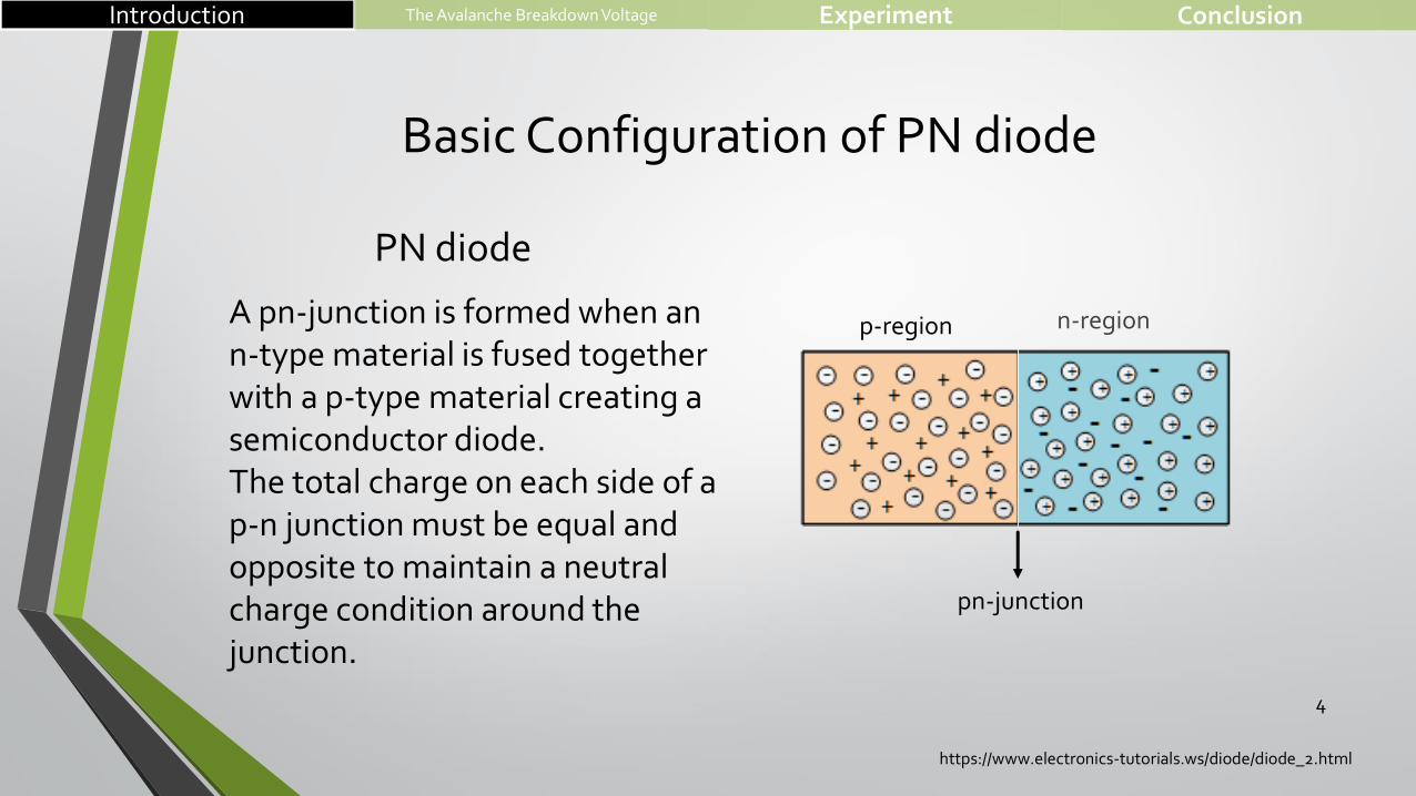
A pn-junction is formed when an n-type material is fused together with a p-type material creating a semiconductor diode.The total charge on each side of a p-n junction must be equal and opposite to maintain a neutral charge condition around the junction.
p-region n-region
pn-junction
https://www.electronics-tutorials.ws/diode/diode_2.html
Introduction The Avalanche Breakdown Voltage Experiment Conclusion
5
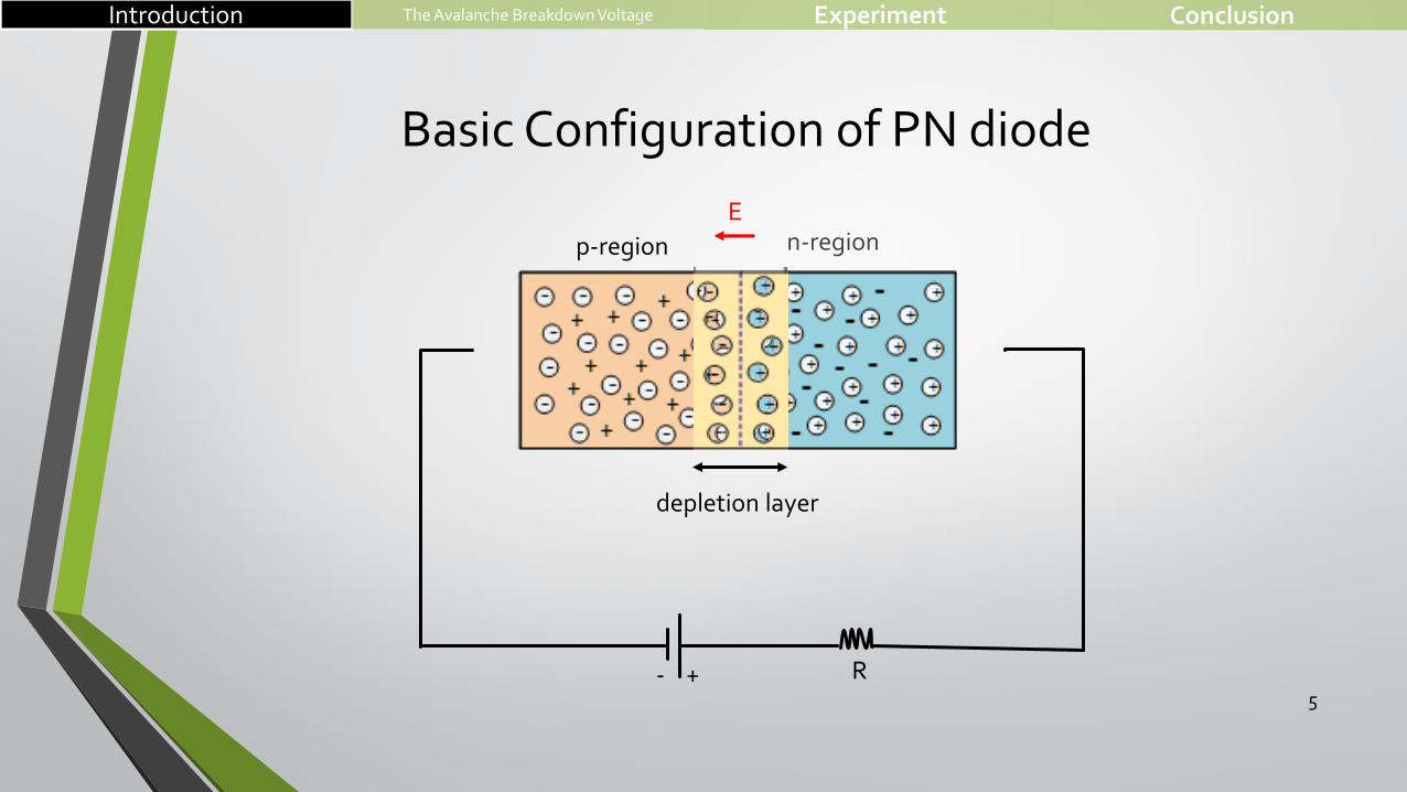
depletion layer
p-region n-region
- + R
Basic Configuration of PN diode
Introduction The Avalanche Breakdown Voltage Experiment Conclusion
E
6
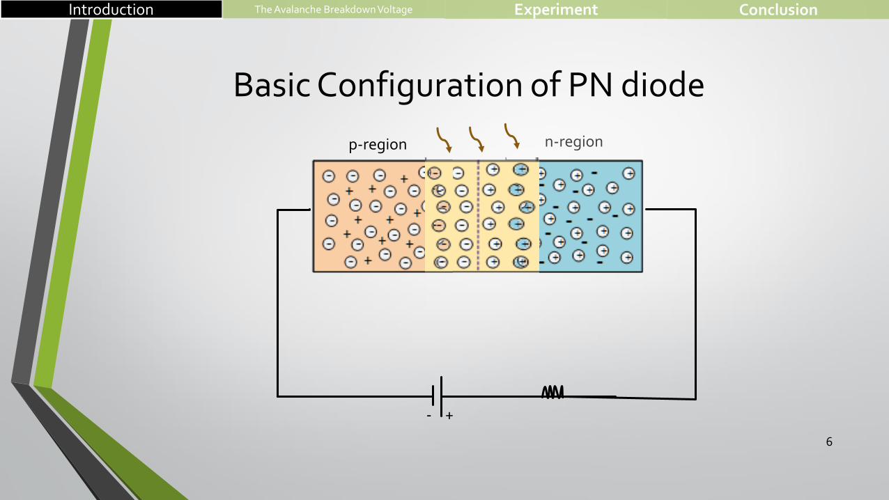
p-region
- +
n-region
Basic Configuration of PN diode
Introduction The Avalanche Breakdown Voltage Experiment Conclusion
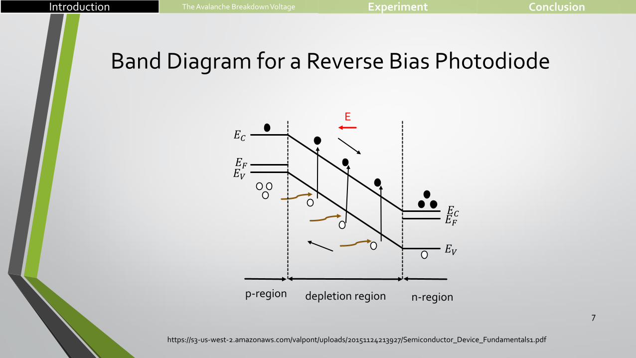
Band Diagram for a Reverse Bias Photodiode
7
𝐸𝐶
𝐸𝐶
𝐸𝑉
𝐸𝑉
𝐸𝐹
𝐸𝐹
p-region depletion region n-region
Introduction The Avalanche Breakdown Voltage Experiment Conclusion
E
https://s3-us-west-2.amazonaws.com/valpont/uploads/20151124213927/Semiconductor_Device_Fundamentals1.pdf
8
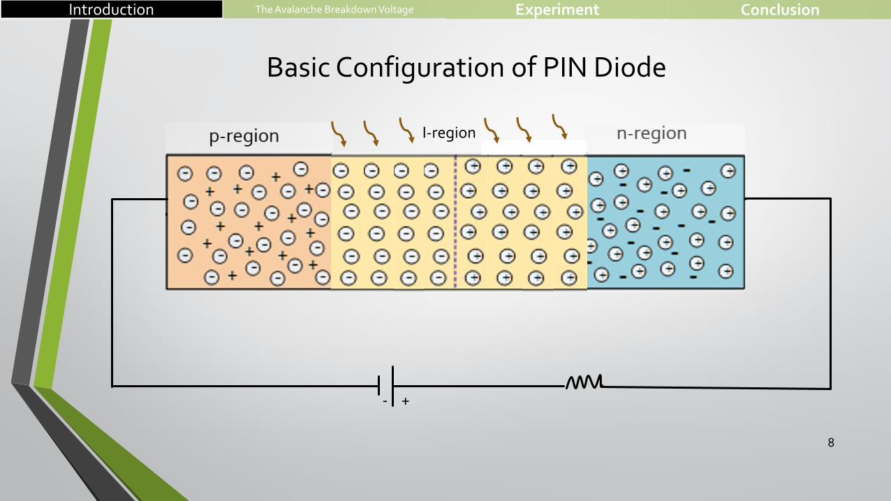
Basic Configuration of PIN Diode
- +
I-region
Introduction The Avalanche Breakdown Voltage Experiment Conclusion
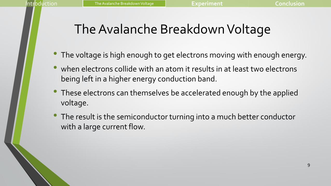
• The voltage is high enough to get electrons moving with enough energy.
• when electrons collide with an atom it results in at least two electrons being left in a higher energy conduction band.
• These electrons can themselves be accelerated enough by the applied voltage.
• The result is the semiconductor turning into a much better conductor with a large current flow.
9
The Avalanche Breakdown Voltage
Introduction The Avalanche Breakdown Voltage Experiment Conclusion
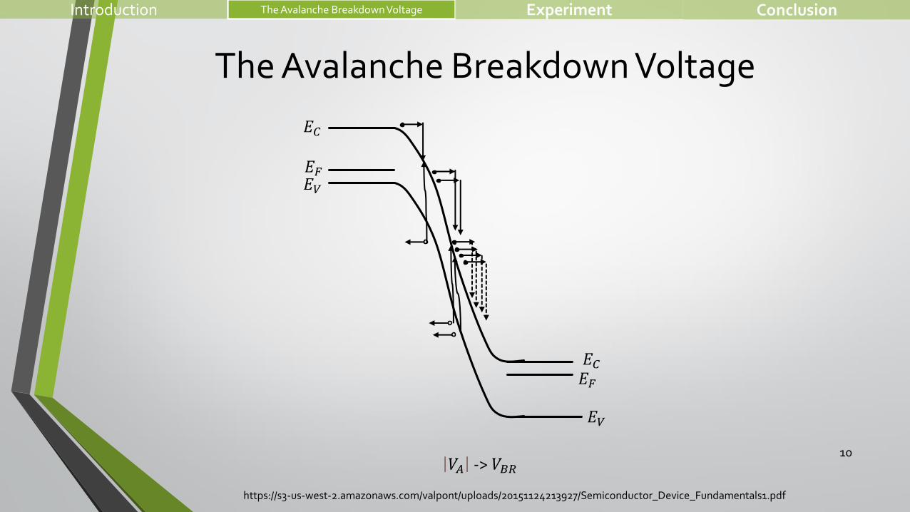
The Avalanche Breakdown Voltage
10
𝐸𝐶
𝐸𝑉
𝐸𝐹
𝐸𝐹
𝐸𝐶
𝐸𝑉
𝑉𝐴 -> 𝑉𝐵𝑅
Introduction The Avalanche Breakdown Voltage Experiment Conclusion
https://s3-us-west-2.amazonaws.com/valpont/uploads/20151124213927/Semiconductor_Device_Fundamentals1.pdf
The structure of PIN device
11
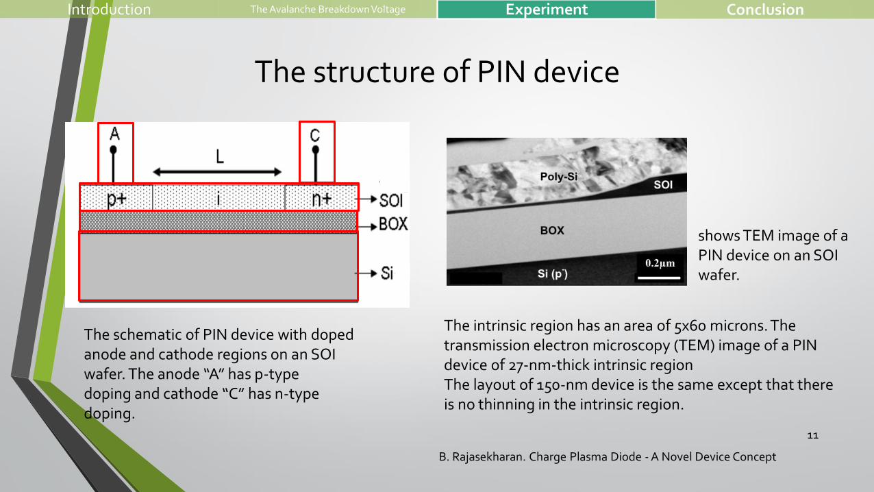
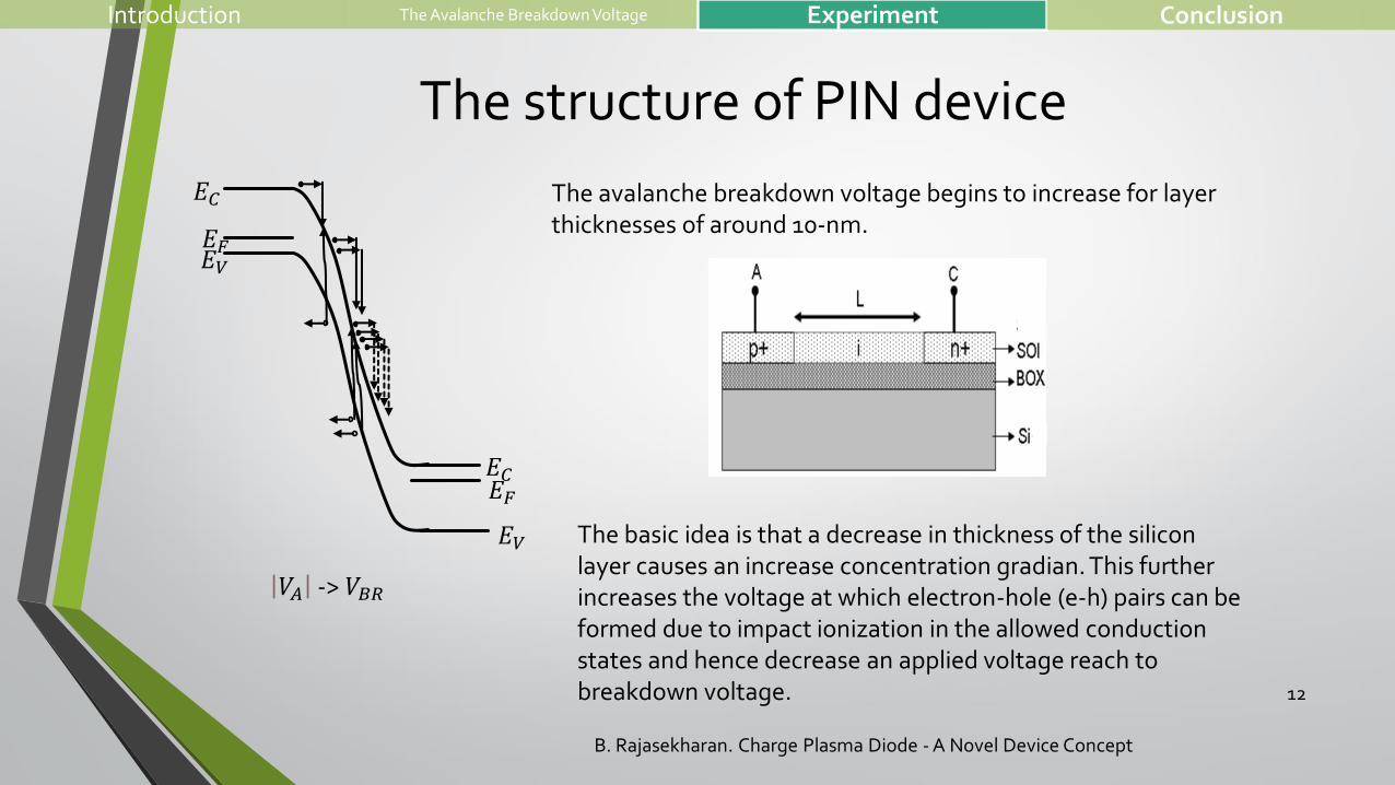
The schematic of PIN device with doped anode and cathode regions on an SOI wafer. The anode “A” has p-type doping and cathode “C” has n-type doping.
shows TEM image of a PIN device on an SOI wafer.
The intrinsic region has an area of 5x60 microns. The transmission electron microscopy (TEM) image of a PIN device of 27-nm-thick intrinsic regionThe layout of 150-nm device is the same except that there is no thinning in the intrinsic region.
Introduction The Avalanche Breakdown Voltage Experiment Conclusion
B. Rajasekharan. Charge Plasma Diode - A Novel Device Concept
The structure of PIN device
12
𝐸𝐶
𝐸𝑉
𝐸𝐹
𝐸𝐹
𝐸𝐶
𝐸𝑉
𝑉𝐴 -> 𝑉𝐵𝑅
The avalanche breakdown voltage begins to increase for layer thicknesses of around 10-nm.
The basic idea is that a decrease in thickness of the silicon layer causes an increase concentration gradian. This further increases the voltage at which electron-hole (e-h) pairs can be formed due to impact ionization in the allowed conduction states and hence decrease an applied voltage reach to breakdown voltage.
Introduction The Avalanche Breakdown Voltage Experiment Conclusion
B. Rajasekharan. Charge Plasma Diode - A Novel Device Concept
Breakdown Voltage Characteristic Equation
13
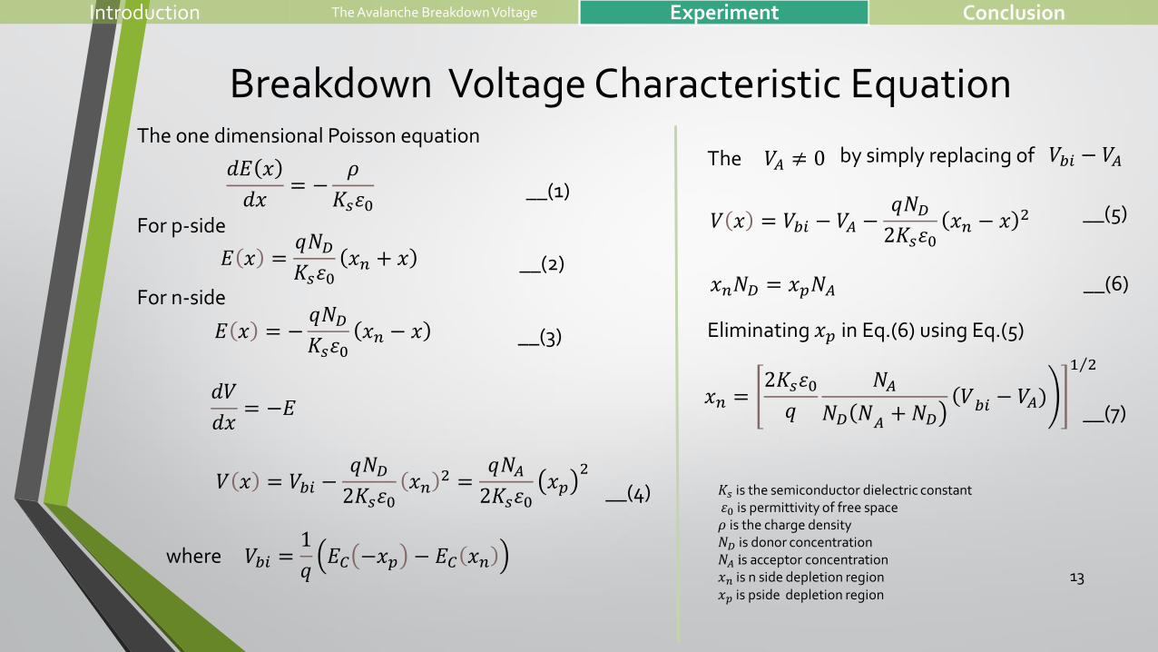
𝑑𝐸 𝑥
𝑑𝑥= −
𝜌
𝐾𝑠𝜀0
𝐸 𝑥 = −𝑞𝑁𝐷𝐾𝑠𝜀0
𝑥𝑛 − 𝑥
𝑑𝑉
𝑑𝑥= −𝐸
𝑉 𝑥 = 𝑉𝑏𝑖 −𝑞𝑁𝐷2𝐾𝑠𝜀0
𝑥𝑛2 =
𝑞𝑁𝐴2𝐾𝑠𝜀0
𝑥𝑝2
𝑥𝑛𝑁𝐷 = 𝑥𝑝𝑁𝐴
𝑉 𝑥 = 𝑉𝑏𝑖 − 𝑉𝐴 −𝑞𝑁𝐷2𝐾𝑠𝜀0
𝑥𝑛 − 𝑥 2
𝑥𝑛 = ൱2𝐾𝑠𝜀0𝑞
𝑁𝐴
൯𝑁𝐷ሺ𝑁𝐴 + 𝑁𝐷ሺ𝑉𝑏𝑖 − 𝑉𝐴)
Τ1 2
𝑉𝑏𝑖 =1
𝑞𝐸𝐶 −𝑥𝑝 − 𝐸𝐶 𝑥𝑛
𝑉𝐴 ≠ 0
𝐸 𝑥 =𝑞𝑁𝐷𝐾𝑠𝜀0
𝑥𝑛 + 𝑥
where
For p-side
For n-side
__(1)
__(2)
__(3)
__(4)
__(5)
__(6)
__(7)
The one dimensional Poisson equationThe by simply replacing of 𝑉𝑏𝑖 − 𝑉𝐴
Eliminating 𝑥𝑝 in Eq.(6) using Eq.(5)
Introduction The Avalanche Breakdown Voltage Experiment Conclusion
𝐾𝑠 is the semiconductor dielectric constant𝜀0 is permittivity of free space𝜌 is the charge density𝑁𝐷 is donor concentration 𝑁𝐴 is acceptor concentration𝑥𝑛 is n side depletion region𝑥𝑝 is pside depletion region
14
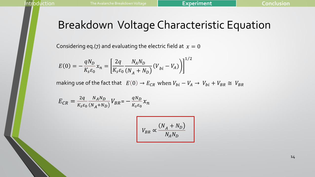
𝑥 = 0
𝐸 0 = −𝑞𝑁𝐷𝐾𝑠𝜀0
𝑥𝑛 = ቇ2𝑞
𝐾𝑠𝜀0
𝑁𝐴𝑁𝐷
൯ሺ𝑁𝐴 + 𝑁𝐷ሺ𝑉𝑏𝑖 − 𝑉𝐴)
Τ1 2
𝐸 0 → 𝐸𝐶𝑅 when 𝑉𝑏𝑖 − 𝑉𝐴 → 𝑉𝑏𝑖 + 𝑉𝐵𝑅 ≅ 𝑉𝐵𝑅
𝐸𝐶𝑅 =2𝑞
𝐾𝑠𝜀0
𝑁𝐴𝑁𝐷
൯ሺ𝑁𝐴+𝑁𝐷𝑉𝐵𝑅= −
𝑞𝑁𝐷
𝐾𝑠𝜀0𝑥𝑛
𝑉𝐵𝑅 ∝൯ሺ𝑁𝐴 + 𝑁𝐷
𝑁𝐴𝑁𝐷
Considering eq.(7) and evaluating the electric field at
making use of the fact that
Breakdown Voltage Characteristic Equation
Introduction The Avalanche Breakdown Voltage Experiment Conclusion
Result: The Avalanche BV Characteristic
15
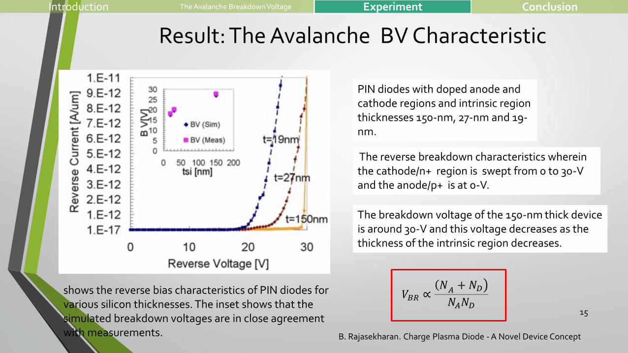
shows the reverse bias characteristics of PIN diodes for various silicon thicknesses. The inset shows that the simulated breakdown voltages are in close agreement with measurements.
Introduction The Avalanche Breakdown Voltage Experiment Conclusion
PIN diodes with doped anode and cathode regions and intrinsic region thicknesses 150-nm, 27-nm and 19-nm.
The reverse breakdown characteristics wherein the cathode/n+ region is swept from 0 to 30-V and the anode/p+ is at 0-V.
The breakdown voltage of the 150-nm thick device is around 30-V and this voltage decreases as the thickness of the intrinsic region decreases.
𝑉𝐵𝑅 ∝൯ሺ𝑁𝐴 + 𝑁𝐷
𝑁𝐴𝑁𝐷
B. Rajasekharan. Charge Plasma Diode - A Novel Device Concept
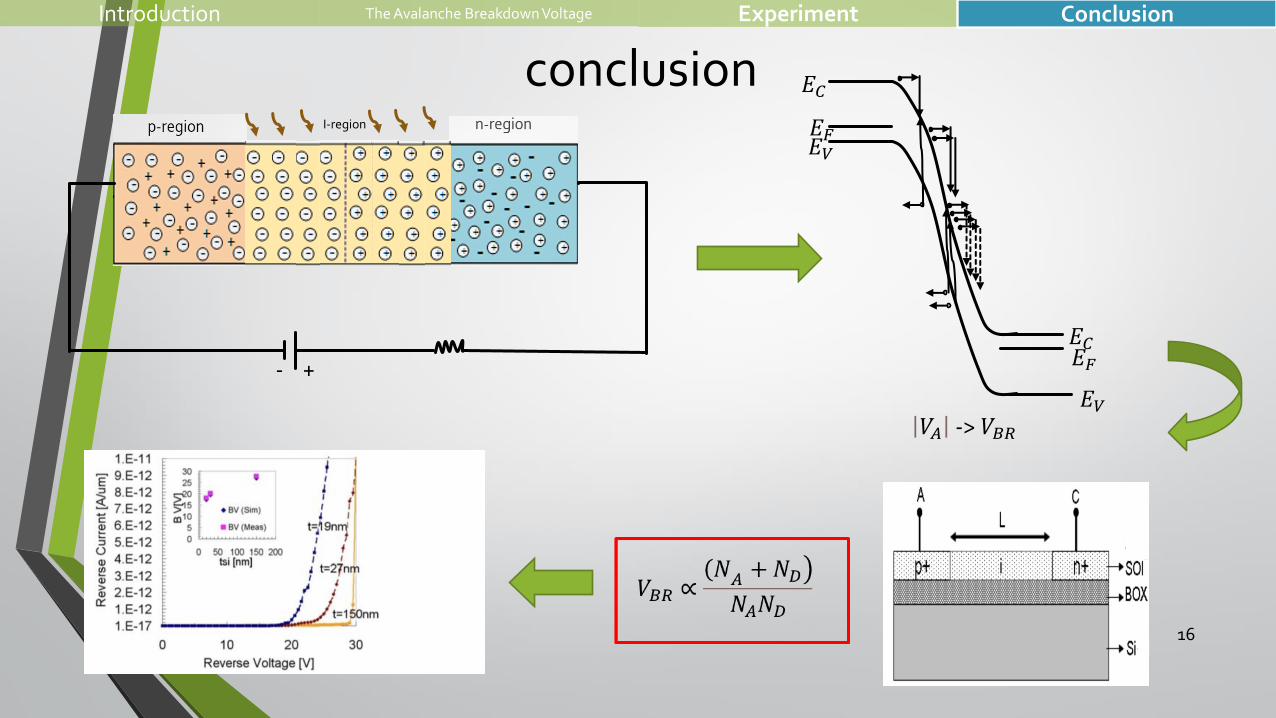
conclusion
16
Introduction The Avalanche Breakdown Voltage Experiment Conclusion
𝐸𝐶
𝐸𝑉
𝐸𝐹
𝐸𝐹
𝐸𝐶
𝐸𝑉
𝑉𝐴 -> 𝑉𝐵𝑅
- +
I-region
Reference
17
• B. Rajasekharan. Charge Plasma Diode - A Novel Device Concept. in Proceedings of the 11th annual workshop on semiconductor advances for future electronics and sensors (SAFE), Technology Foundation STW, Dec. 2008, pp. 576–579.
• https://s3-us-west-2.amazonaws.com/valpont/uploads/20151124213927/Semiconductor_Device_Fundamentals1.pdf
• https://www.electronics-tutorials.ws/diode/diode_2.html
• https://www.halbleiter.org/en/waferfabrication/doping
• https://www.microsemi.com/sites/default/files/datasheets/Products/rf/APPENDIX%20F.pdf
• https://byjus.com/physics/pin-diode/
Acknowledgement
• Dr. Wittawat Yamwong
Thai Microelectronics Center (TMEC)
51/4 Moo 1 Suwintawong Road, Wangtakien,
Muang, Chachoengsao 24000, Thailand
• Dr.Poompong Chaiwongkhot
Department of Physics, Faculty of Science,
Mahidol University, Bangkok, Thailand
• Assistant Professor Dr. Kritsanu Tivakornsasithorn
Department of Physics, Faculty of Science,
Mahidol University, Bangkok, Thailand 18
The Avalanche Breakdown Voltage of PIN DiodeBy
Pathompron Jaikwang SCPY/B 6105012
Department of Physics, Faculty of Science, Mahidol University
Email : [email protected]
19
THANK YOU