Design Optimization of α SiC based ATT diode for harmonic ...
5
Design Optimization of α SiC based ATT diode for harmonic mode operation Debraj Chakraborty 1,a , Moumita Mukherjee 2,b 1 Department of ECE,Pailan Colllege of Management & Technology, Kolkata-700104, West Bengal, India 2 Department of Physics, Adamas University, Kolkata-700126, West Bengal, India a [email protected], b [email protected] Keywords: Avalanche Transit Time Device, Harmonic power generation, Terahertz source, Quantum corrected drift diffusion model, Large signal non-linear model. Abstract: The paper deals with design and analysis of Si/4H-SiC superlattice based Avalanche Transit time (ATT) device operating at Terahertz frequency region. A generalised non-linear quantum drift diffusion model is developed for the analysis. The authors have studied the higher harmonic effects on the high frequency performances. It is observed that due to the superlattice structure, the device is capable of generating a considerable amount of power (~100 mW) even at 3rd harmonic oscillation. The device is oscillating at fundamental mode of frequency ~ 0.5 THz with an efficiency of ~ 10% The authors have made the analysis realistic by incorporating the temperature dependent carrier ionization rate, saturation drift velocity, mobility and effective mass. To the best of authors’ knowledge, this is the first report on higher THz region harmonic analysis of Si/4H-SiC superlattice-ATT device. 1. Introduction The terahertz (THz) regime (0.1-10 THz) is rich with emerging possibilities in remote sensing, imaging and communications, with unique applications for detecting hidden biological weapons and explosives. Since the last decade scientists working in this area are showing significant interest to develop solid state sources that may generate THz power. Among all two-terminal semiconductor devices (Gunn, IMPATT, TRAPATT, BARITT etc.), IMPATT devices have already emerged as the most efficient solid state sources that can deliver highest RF power even at 300 GHz [1]. Although the conventional IMPATT diodes fabricated on GaAs (Gallium Arsenide) and Si (Silicon) are found to be reliable, these are limited by power and operating frequencies due to the fundamental limitations of the material parameters. On the other hand, wide band gap semiconductor like SiC (Silicon Carbide) and compounds based on it have excellent material properties that can be explored to develop high power and high frequency IMPATT devices. The authors have therefore designed IMPATT diode based on superlattice Si/SiC, since this material pair offers (i) 10 times higher Ec, and (ii) 2 times higher vs in comparison to those of Si and GaAs . Si/SiC superlattice has an energy band gap of 3.4 eV at room temperature. This high value of the energy band gap in the superlattice enables the devices based on this material pair to support peak Journal of Physics Through Computation (2019) Vol. 2: 21-25 Clausius Scientific Press, Canada DOI: 10.23977/jptc.2019.21005 ISSN 2617-1163 21
Transcript of Design Optimization of α SiC based ATT diode for harmonic ...
Design Optimization of α SiC based ATT diode for harmonic mode operation
Debraj Chakraborty1,a, Moumita Mukherjee2,b 1Department of ECE,Pailan Colllege of Management & Technology, Kolkata-700104, West Bengal,
India 2Department of Physics, Adamas University, Kolkata-700126, West Bengal, India
[email protected], [email protected]
Keywords: Avalanche Transit Time Device, Harmonic power generation, Terahertz source, Quantum corrected drift diffusion model, Large signal non-linear model.
Abstract: The paper deals with design and analysis of Si/4H-SiC superlattice based Avalanche Transit time (ATT) device operating at Terahertz frequency region. A generalised non-linear quantum drift diffusion model is developed for the analysis. The authors have studied the higher harmonic effects on the high frequency performances. It is observed that due to the superlattice structure, the device is capable of generating a considerable amount of power (~100 mW) even at 3rd harmonic oscillation. The device is oscillating at fundamental mode of frequency ~ 0.5 THz with an efficiency of ~ 10% The authors have made the analysis realistic by incorporating the temperature dependent carrier ionization rate, saturation drift velocity, mobility and effective mass. To the best of authors’ knowledge, this is the first report on higher THz region harmonic analysis of Si/4H-SiC superlattice-ATT device.
1. Introduction
The terahertz (THz) regime (0.1-10 THz) is rich with emerging possibilities in remote sensing,imaging and communications, with unique applications for detecting hidden biological weapons and explosives. Since the last decade scientists working in this area are showing significant interest to develop solid state sources that may generate THz power. Among all two-terminal semiconductor devices (Gunn, IMPATT, TRAPATT, BARITT etc.), IMPATT devices have already emerged as the most efficient solid state sources that can deliver highest RF power even at 300 GHz [1]. Although the conventional IMPATT diodes fabricated on GaAs (Gallium Arsenide) and Si (Silicon) are found to be reliable, these are limited by power and operating frequencies due to the fundamental limitations of the material parameters. On the other hand, wide band gap semiconductor like SiC (Silicon Carbide) and compounds based on it have excellent material properties that can be explored to develop high power and high frequency IMPATT devices. The authors have therefore designed IMPATT diode based on superlattice Si/SiC, since this material pair offers (i) 10 times higher Ec, and (ii) 2 times higher vs in comparison to those of Si and GaAs . Si/SiC superlattice has an energy band gap of 3.4 eV at room temperature. This high value of the energy band gap in the superlattice enables the devices based on this material pair to support peak
Journal of Physics Through Computation (2019) Vol. 2: 21-25 Clausius Scientific Press, Canada
DOI: 10.23977/jptc.2019.21005 ISSN 2617-1163
21
internal electric field (EC) about ten times higher than Si and GaAs. The fabrication of ATT device at Terahertz region is complex and costly. Though the authors have earlier attempted for the fabrication of such devices, but due to the narrowing of avalanche region / drift region, the fabrication becomes a complex phenomenon. The authors in this paper have addressed the issue by introducing harmonic effects on the high frequency performance of the device. The device is operating at 0.5 THz at fundamental mode of operation. However, by tuning the circuit, the device could be operated even at > 1.0 THz with a moderate to higher power output. The authors have developed a self consistent; quasi-2D non-linear, voltage –driven Large Signal (L-S) simulator for designing superlattice Avalanche Transit Time (ATT) device. The simulator incorporates the effects of inter-sub-band tunneling, hot carrier effect, quantum size effect, realistic field and temperature dependent carrier density, mobility in superlattice active region. Also the saturation velocity as a function of reverse bias field has been incorporated in the present analysis. To the best of authors’ knowledge this is the first ever report on harmonic effects in super-lattice THz-IMPATT.
2. Methodology
This section will deal with the simulation methodology, necessary boundary conditions and the device structure details.
2.1 Quantum Modified Classical Drift-Diffusion (QMCLDD) model
Large signal analysis of IMPATT diodes is an essential prerequisite for perfect design and implementation of THz oscillators. The generalization, accuracy and efficiency of the study have become very popular through the decades [1-7]. Numerical solutions are preferred over analytical modelling of large signal performance, since tremendous non-linear processing occur within this device structure. Present study of complete analysis involves generalised & non-linear simulation of DDR type (p+pnn+) heterostructure IMPATT device, excluded from any abrupt assumption. This, heterostructure is mainly developed by Si/ 4HSiC.
The present model is based upon self consistent single harmonic analysis of IMPATT device, where the slightly changed “field-maximum method”[8] is assigned for producing detail analysis of Electric field profile in snap-shot mode, carrier current density depending upon the width of active region for a full cycle of oscillation. The non-linear model, associated in this program, comprises of differential equations describing particle concentrations, equations highlighting current density, ionization rates of the carrier which are field-dependent & many other effects including depletion charges etc. The drift velocity of charge-carriers within a specific range of temperature is also considered.
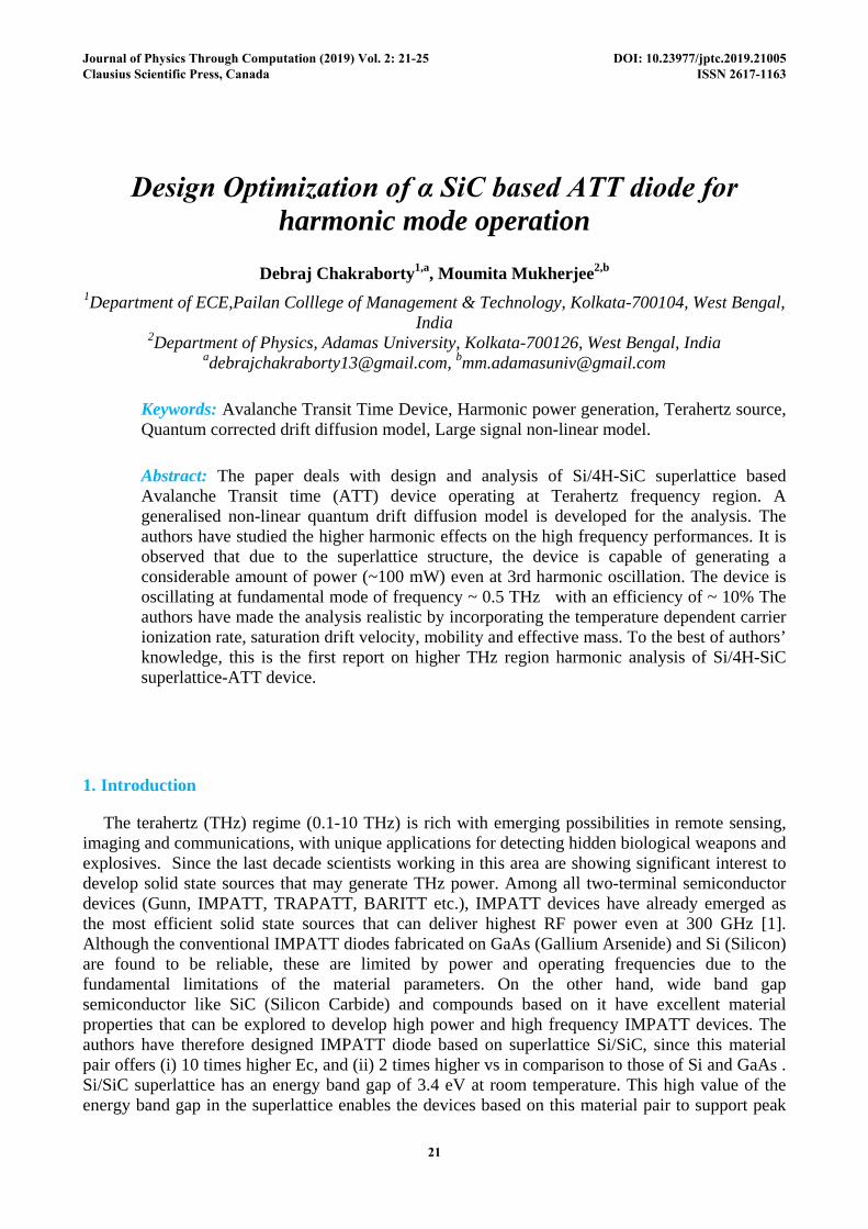
A Quantum Corrected Drift Diffusion (QCDD) model is employed for high modulation analysis. An electric field following a sinusoidal variation of the form ξ= ξ0 + mi ξ0sinωt, where ξ0 is the time-invariant maximum field value and mi is modulation index. The modulation index is changed to obtain large signal effect of IMPATT diode.
Figure1. Hetero-structure p-n junction ATT diode active region under reverse bias operation
22
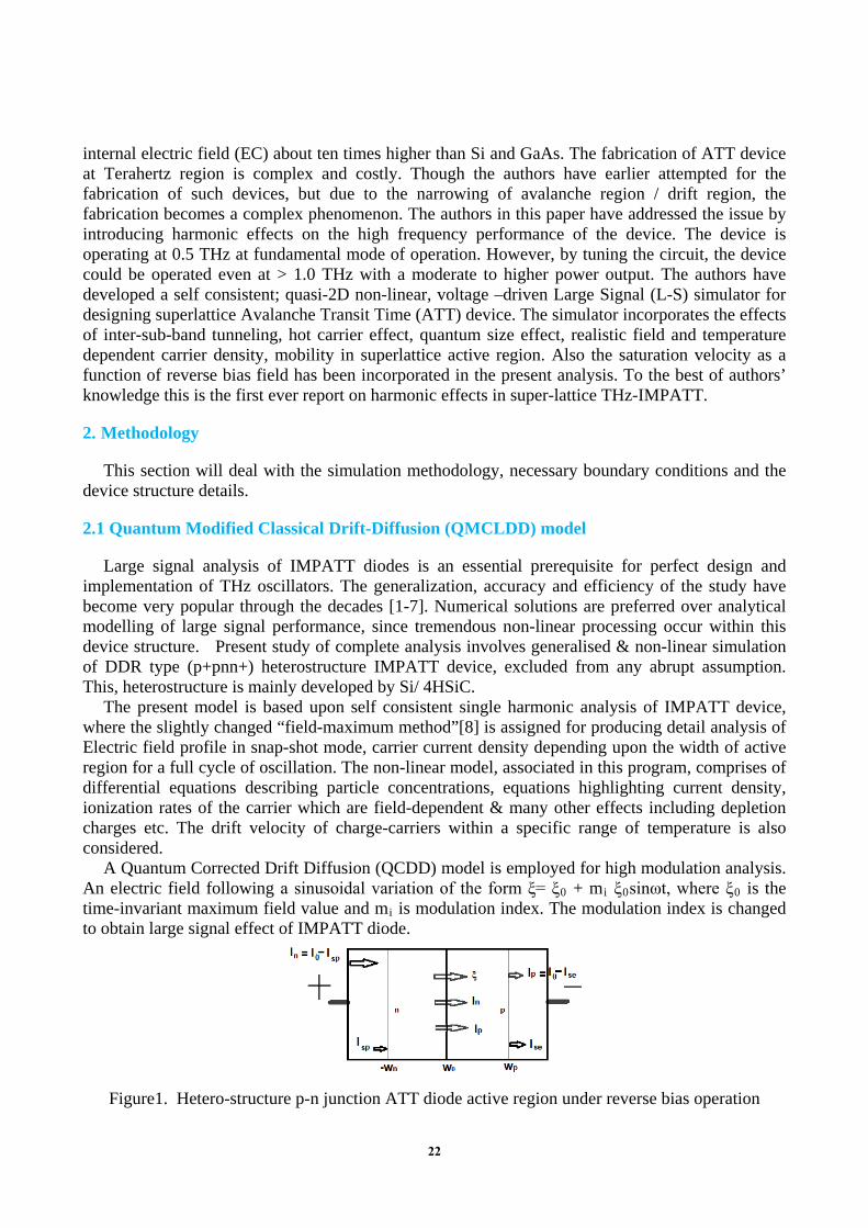
The heterostructure Si/4HSiC IMPATT simulation effects are presented here, where transport mechanism within the mesa structure is considered to be directed along the symmetry axis. The equivalent circuit is shown in Figure 1. Instantaneous electric field profile in the course of oscillation is a keynote of the analysis. A precise & effective single harmonic model [9] is analysed to develop impedance & admittance characteristics of the device depending upon signal amplitude in THz frequency range. As depicted in Figure 2, the mode of biasing is DC which is coupled to an AC supply within a finite extent, so that, mathematically it is expressed as ϕt = ϕdc + ϕrf sin (ωt + ψ) , ‘ω’ being the operating frequency & ‘ψ’ is the beginning phase angle. Complete current of the diode therefore including both DC & AC components, is given by:
Figure 2. Display of peripheral current and voltage of IMPATT diode, Cdep = depletion region capacitance, χd = diode admittance, χc = circuit admittance
= - ) + (1)
The expression for diode admittance χd, depending on the oscillation frequency ω is given by
= + - - (2)
Where is a constant and is the avalanche frequency. The simulation is conducted over large space & changing the meshes. For operating frequency at
maximum values, the output power is obtained using the expression,
(3)
Here is the conductance (negative) at the top frequency.
3. Results and Discussions
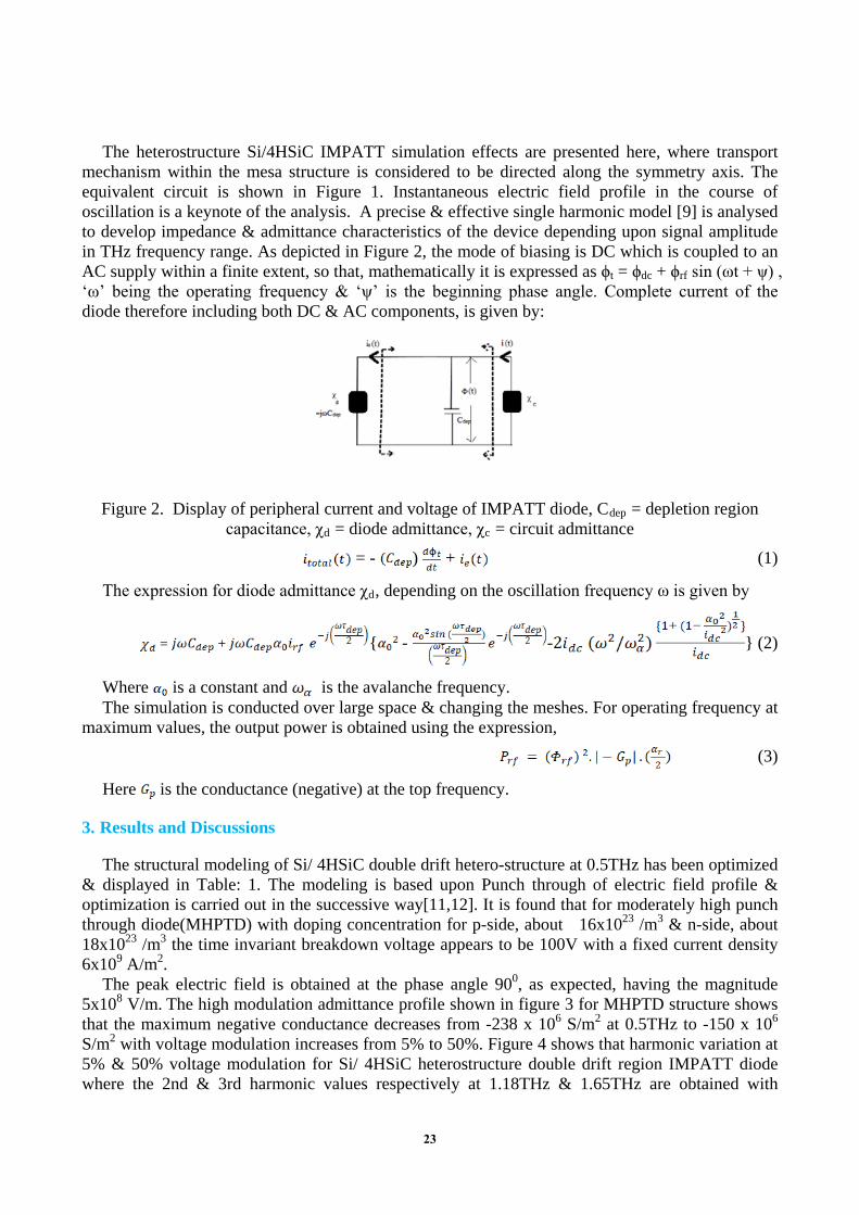
The structural modeling of Si/ 4HSiC double drift hetero-structure at 0.5THz has been optimized & displayed in Table: 1. The modeling is based upon Punch through of electric field profile & optimization is carried out in the successive way[11,12]. It is found that for moderately high punch through diode(MHPTD) with doping concentration for p-side, about 16x1023 /m3 & n-side, about 18x1023 /m3 the time invariant breakdown voltage appears to be 100V with a fixed current density 6x10⁹ A/m2.
The peak electric field is obtained at the phase angle 900, as expected, having the magnitude 5x10⁸ V/m. The high modulation admittance profile shown in figure 3 for MHPTD structure shows that the maximum negative conductance decreases from -238 x 106 S/m2 at 0.5THz to -150 x 106 S/m2 with voltage modulation increases from 5% to 50%. Figure 4 shows that harmonic variation at 5% & 50% voltage modulation for Si/ 4HSiC heterostructure double drift region IMPATT diode where the 2nd & 3rd harmonic values respectively at 1.18THz & 1.65THz are obtained with
23
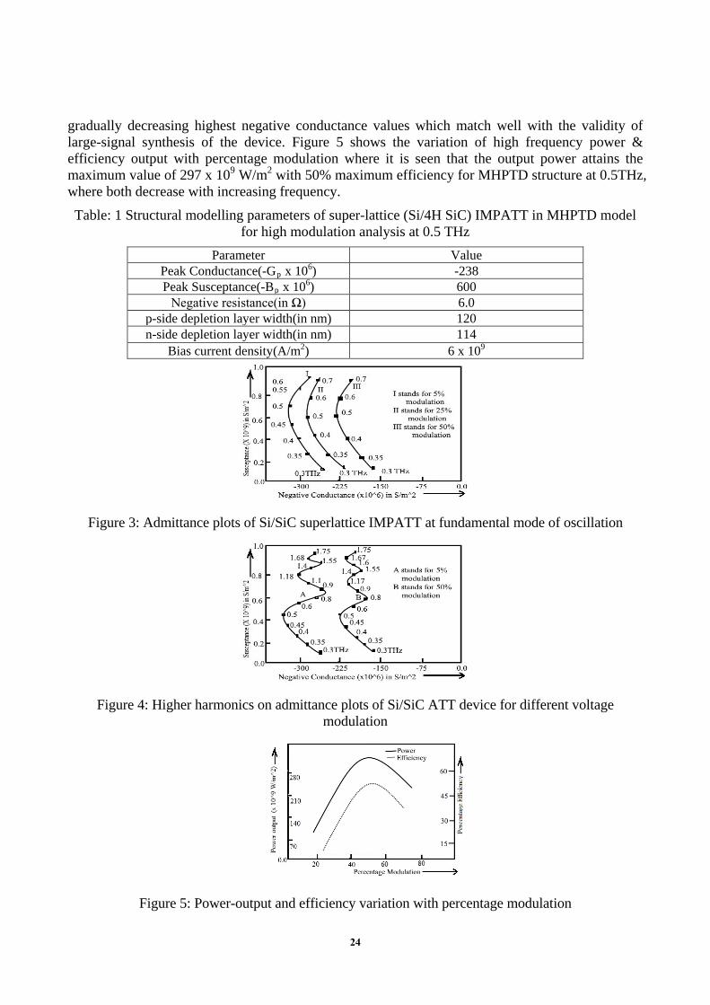
gradually decreasing highest negative conductance values which match well with the validity of large-signal synthesis of the device. Figure 5 shows the variation of high frequency power & efficiency output with percentage modulation where it is seen that the output power attains the maximum value of 297 x 109 W/m2 with 50% maximum efficiency for MHPTD structure at 0.5THz, where both decrease with increasing frequency. Table: 1 Structural modelling parameters of super-lattice (Si/4H SiC) IMPATT in MHPTD model
for high modulation analysis at 0.5 THz Parameter Value
Peak Conductance(-Gp x 106) -238 Peak Susceptance(-Bp x 106) 600
Negative resistance(in Ω) 6.0 p-side depletion layer width(in nm) 120 n-side depletion layer width(in nm) 114
Bias current density(A/m2) 6 x 10⁹
Figure 3: Admittance plots of Si/SiC superlattice IMPATT at fundamental mode of oscillation
Figure 4: Higher harmonics on admittance plots of Si/SiC ATT device for different voltage
modulation
Figure 5: Power-output and efficiency variation with percentage modulation
24
4. Conclusion
The authors have studied and reported the large signal modeling of Si/SiC super-lattice ATT device incorporating the higher harmonic effects. The generalized simulation technique, incorporating physics as much as possible, is developed by the authors. Effect of higher harmonic on THz admittance plots is studied and it is found that due to the super-lattice structure harmonic effects are considerably good in Si/SiC devices. To the best of the author’s knowledge this is the first report on hetero-structure IMPATT at this frequency level with the proposed super-lattice Si/4H-SiC.
References
[1] Eric R. Mueller(2003) Terahertz Radiation: Applications and Sources. The Industrial Physicist, August/ September, 27-29.[2] Blue J L(1969) Approximate large-signal analysis of IMPATT oscillators.Bell Syst Tech J413, 2, 38.[3] Schroeder W E, Haddad G I( 1973) Nonlinear properties of IMPATT devices. Proc IEEE, 61, 153.[4] Grierson J R, O’Hara S(1973) A comparison of silicon and gallium arsenide large-signal IMPATT diode behaviourbetween 10 and 100 GHz. Solid-State Electron, 16, 719.[5] Mathur P C, Sharma V(1976) Large signal analysis of IMPATT diodes. Physica Status Solidi A, 36(1), 269.[6] Thomson I(1972) Large signal analysis of abrupt junction silicon IMPATT diode. International Journal ofElectronics, 32(2), 121.[7] Scharfetter D L, Gummel H K(1969) Large signal analysis of a silicon read diode oscillator. IEEE Trans ElectronDevices, ED-16(1), 64.[8] Roy S K, Banerjee J P, Pati S P (1985)A computer analysis of the distribution of high frequency negative resistancein the depletion layer of IMPATT diodes. Proc 4th Conf on Num Anal of Semiconductor Devices Dublin: Boole,NASECODE IV, 494.[9] Gupta Madhu – Sudan and Lomax Ronald J(April 1973) A Current –Excited Large Signal Analysis of IMPATTDevices and Its Circuit Implications . IEEE Transactions on Electron Devices, ED-20,4.[10] Mukherjee M, Tripathy P R, Pati S P(2011) Asymmetrical homojunction and heterojunction transit time devicesbased on Si/Ge and Ge/Si material systems—a comparative analysis at MM-wave frequencies. Journal ofSemiconductors, 32(11), 113001.[11] Mukherjee M, Majumder N, Roy S K, Goswami K(26 October 2007) GaN IMPATT diode: a photo-sensitive highpower terahertz source. Semiconductor Science and Technology-2007 IOP Publishing Ltd, 22,12.[12] Pattanaik S R, Dash G N and Mishra J K(17 February 2005) Prospects of 6H-SiC for operation as an IMPATTdiode at 140 GHz. Semiconductor Science and Technology-2005 IOP Publishing Ltd,2(3).
25