RRQ030P03 : Transistors Breakdown voltage temperature coefficient ΔV (BR)DSS ΔT j I D = -1mA...
12
Datasheet www.rohm.com © 2012 ROHM Co., Ltd. All rights reserved. RRQ030P03 Pch -30V -3A Power MOSFET lOutline V DSS -30V TSMT6 R DS(on) (Max.) 75mW I D -3A P D 1.25W lFeatures lInner circuit 1) Low on - resistance. 2) Built-in G-S Protection Diode. 3) Small Surface Mount Package (TSMT6). 4) Pb-free lead plating ; RoHS compliant lPackaging specifications Type Packaging Taping lApplication Reel size (mm) 180 DC/DC converters Tape width (mm) 8 Basic ordering unit (pcs) 3,000 Drain - Source voltage V DSS -30 V Taping code TR Marking UA lAbsolute maximum ratings(T a = 25°C) Parameter Symbol Value Unit Continuous drain current I D *1 3 A Pulsed drain current I D,pulse *2 12 A Power dissipation Gate - Source voltage V GSS 20 V P D *3 1.25 W P D *4 0.6 W Junction temperature T j 150 °C Range of storage temperature T stg -55 to +150 °C (2) (1) (4) (3) (5) (6) *1 ESD PROTECTION DIODE *2 BODY DIODE (1) Drain (2) Drain (3) Gate (4) Source (5) Drain (6) Drain 1/11 2012.09 - Rev.B
Transcript of RRQ030P03 : Transistors Breakdown voltage temperature coefficient ΔV (BR)DSS ΔT j I D = -1mA...

Datasheet
www.rohm.com© 2012 ROHM Co., Ltd. All rights reserved.
RRQ030P03 Pch -30V -3A Power MOSFET
lOutline
VDSS -30VTSMT6
RDS(on) (Max.) 75mW
ID -3APD 1.25W
lFeatures lInner circuit
1) Low on - resistance.
2) Built-in G-S Protection Diode.
3) Small Surface Mount Package (TSMT6).
4) Pb-free lead plating ; RoHS compliant
lPackaging specifications
Type
Packaging Taping
lApplication Reel size (mm) 180
DC/DC converters Tape width (mm) 8
Basic ordering unit (pcs) 3,000
Drain - Source voltage VDSS -30 V
Taping code TR
Marking UA
lAbsolute maximum ratings(Ta = 25°C)
Parameter Symbol Value Unit
Continuous drain current ID *1
3 A
Pulsed drain current ID,pulse *2
12 A
Power dissipation
Gate - Source voltage VGSS 20 V
PD *3 1.25 W
PD *4 0.6 W
Junction temperature Tj 150 °C
Range of storage temperature Tstg -55 to +150 °C
(2)
(1)
(4)
(3)
(5) (6)
*1 ESD PROTECTION DIODE *2 BODY DIODE
(1) Drain (2) Drain (3) Gate (4) Source (5) Drain (6) Drain
1/11 2012.09 - Rev.B
www.rohm.com© 2012 ROHM Co., Ltd. All rights reserved.
Data SheetRRQ030P03
*1 Limited only by maximum temperature allowed.
*2 Pw 10ms, Duty cycle 1%
*3 Mounted on a ceramic board (30×30×0.8mm)
*4 Mounted on a FR4 (15×20×0.8mm)
*5 Pulsed
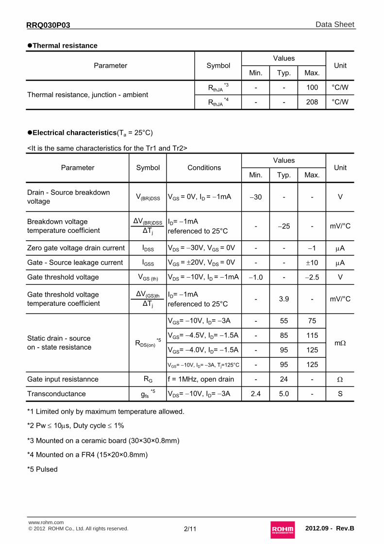
lThermal resistance
Parameter SymbolValues
UnitMin. Typ. Max.
RthJA *4 - - 208 °C/W
RthJA *3 - - 100 °C/W
Thermal resistance, junction - ambient
lElectrical characteristics(Ta = 25°C)
Parameter Symbol ConditionsValues
UnitMin. Typ. Max.
<It is the same characteristics for the Tr1 and Tr2>
V
Breakdown voltagetemperature coefficient
ΔV(BR)DSS
ΔTj
ID= -1mAreferenced to 25°C
- -25 - mV/°C
Drain - Source breakdownvoltage
V(BR)DSS VGS = 0V, ID = -1mA -30 - -
mA
Gate - Source leakage current IGSS VGS = 20V, VDS = 0V - - 10 mA
Zero gate voltage drain current IDSS VDS = -30V, VGS = 0V - - -1
V
Gate threshold voltagetemperature coefficient
ΔV(GS)th
ΔTj
ID= -1mAreferenced to 25°C
- 3.9 - mV/°C
Gate threshold voltage VGS (th) VDS = -10V, ID = -1mA -1.0 - -2.5
Static drain - sourceon - state resistance RDS(on)
*5
VGS= -10V, ID= -3A - 55 75
- 95 125
mWVGS= -4.5V, ID= -1.5A - 85 115
VGS= -4.0V, ID= -1.5A - 95 125
VGS= -10V, ID= -3A, Tj=125°C
W
Transconductance gfs *5 VDS= -10V, ID= -3A 2.4 5.0 - S
Gate input resistannce RG f = 1MHz, open drain - 24 -
2/11 2012.09 - Rev.B

www.rohm.com© 2012 ROHM Co., Ltd. All rights reserved.
Data SheetRRQ030P03
lElectrical characteristics(Ta = 25°C)
Parameter Symbol ConditionsValues
UnitMin. Typ. Max.
<It is the same characteristics for the Tr1 and Tr2>
pFOutput capacitance Coss VDS = -10V - 70 -
Reverse transfer capacitance Crss f = 1MHz
Input capacitance Ciss VGS = 0V - 480 -
- 70 -
UnitMin. Typ. Max.
<It is the same characteristics for the Tr1 and Tr2>
Turn - on delay time td(on) *5 VDD ⋍ -15V, VGS = -10V - 7 -
nsRise time tr
*5 ID = -1.5A - 18 -
Turn - off delay time td(off) *5 RL = 10W - 50 -
VDD ⋍ -15V, ID= -3AVGS = -5V
- 5.2 -
VDD ⋍ -15V, ID= -3AVGS = -10V
- 12 -
-
lGate Charge characteristics(Ta = 25°C)
Parameter Symbol ConditionsValues
Fall time tf *5 RG = 10W - 35
ConditionsValues
UnitMin. Typ. Max.
- 1.6 -
<It is the same characteristics for the Tr1 and Tr2>
lBody diode electrical characteristics (Source-Drain)(Ta = 25°C)
Parameter Symbol
nC
Gate - Drain charge Qgd *5 - 1.6 -
Gate - Source charge Qgs *5
VDD ⋍ -15V, ID= -3AVGS = -5V
Total gate charge Qg *5
- -1.2 V
AInverse diode continuous,forward current IS *1 Ta = 25°C - - -1.0
Forward voltage VSD *5 VGS = 0V, Is = -3A -
3/11 2012.09 - Rev.B
www.rohm.com© 2012 ROHM Co., Ltd. All rights reserved.
Data SheetRRQ030P03
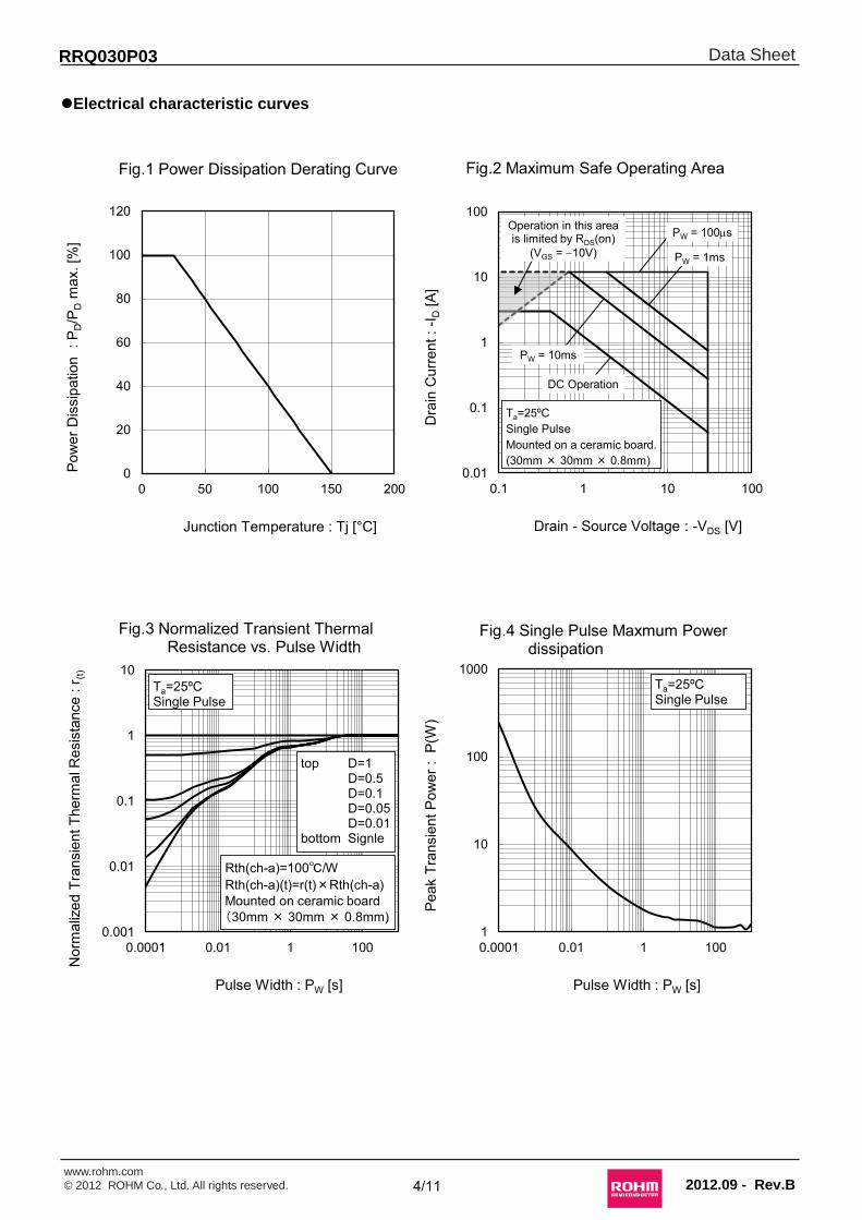
lElectrical characteristic curves
1
10
100
1000
0.0001 0.01 1 100
Ta=25ºC Single Pulse
0.01
0.1
1
10
100
0.1 1 10 100
Ta=25ºC Single Pulse Mounted on a ceramic board. (30mm × 30mm × 0.8mm)
Operation in this area is limited by RDS(on)
(VGS = -10V)
PW = 100ms
PW = 1ms
PW = 10ms
DC Operation
0
20
40
60
80
100
120
0 50 100 150 200
0.001
0.01
0.1
1
10
0.0001 0.01 1 100
Rth(ch-a)=100℃/W Rth(ch-a)(t)=r(t)×Rth(ch-a) Mounted on ceramic board (30mm × 30mm × 0.8mm)
top D=1 D=0.5 D=0.1 D=0.05 D=0.01 bottom Signle
Ta=25ºC Single Pulse
Fig.1 Power Dissipation Derating Curve Fig.2 Maximum Safe Operating Area
Pow
er D
issi
patio
n :
P D/P
D m
ax. [
%]
Dra
in C
urre
nt :
-I D [A
]
Fig.3 Normalized Transient Thermal Resistance vs. Pulse Width
Fig.4 Single Pulse Maxmum Power dissipation
Nor
mal
ized
Tra
nsie
nt T
herm
al R
esis
tanc
e : r
(t)
Pulse Width : PW [s] Pulse Width : PW [s]
Peak
Tra
nsie
nt P
ower
: P
(W)
Junction Temperature : Tj [°C] Drain - Source Voltage : -VDS [V]
4/11 2012.09 - Rev.B

www.rohm.com© 2012 ROHM Co., Ltd. All rights reserved.
Data SheetRRQ030P03
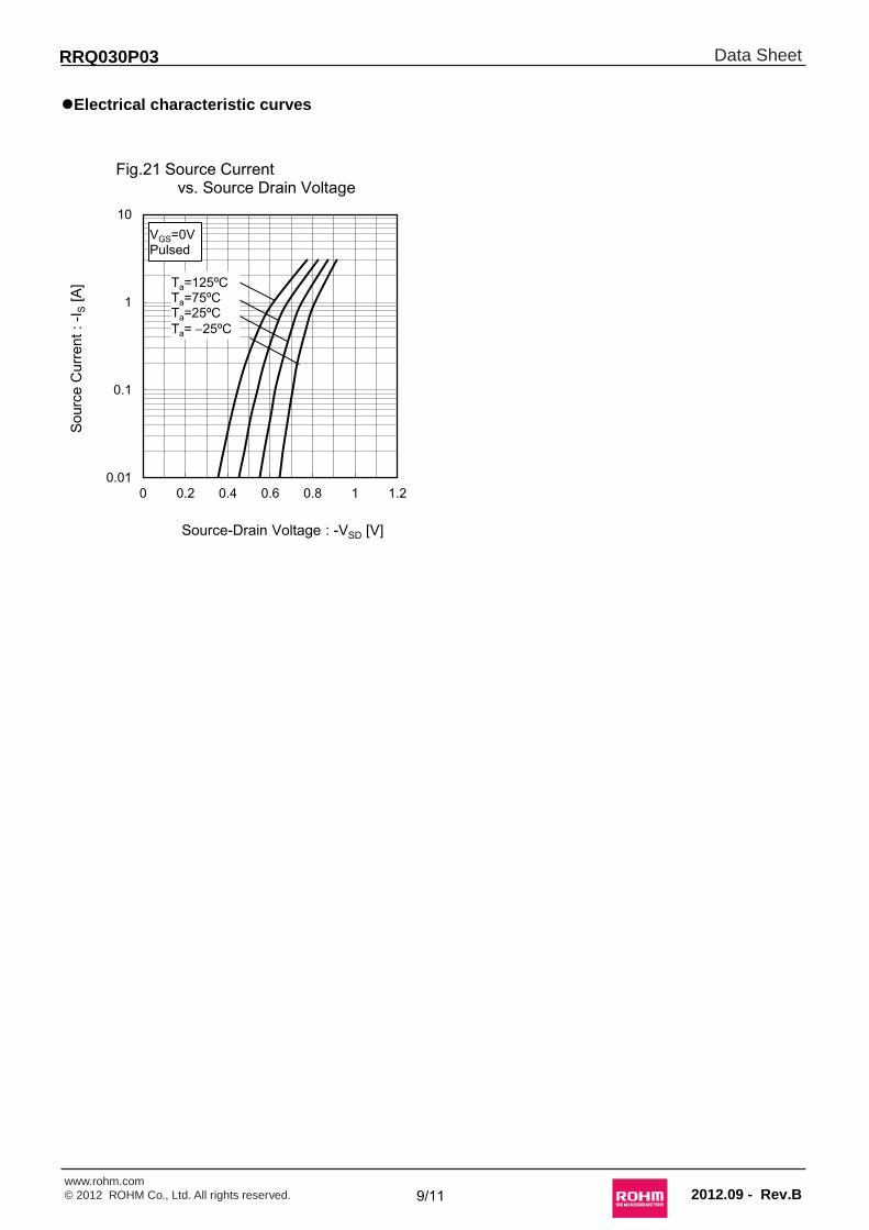
lElectrical characteristic curves
0
20
40
60
-50 0 50 100 150
VGS = 0V ID = -1mA Pulsed
0.001
0.01
0.1
1
10
0 1 2 3 4
Ta= 125ºC Ta= 75ºC Ta= 25ºC Ta= -25ºC
VDS= -10V Pulsed
0
0.5
1
1.5
2
2.5
3
0 0.2 0.4 0.6 0.8 1
VGS= -10.0V
VGS= -3.8V
VGS= -3.2V VGS= -4.5V
VGS= -3.0V
VGS= -2.5V
VGS= -2.8V
0
0.5
1
1.5
2
2.5
3
0 2 4 6 8 10
VGS= -2.8V
VGS= -10.0V
VGS= -3.6V
VGS= -3.0V
VGS= -4.5V
VGS= -3.2V
Ta=25ºC Pulsed
Fig.5 Typical Output Characteristics(I)
Dra
in C
urre
nt :
-I D [A
]
Drain - Source Voltage : -VDS [V]
Fig.6 Typical Output Characteristics(II)
Dra
in C
urre
nt :
-I D [A
]
Drain - Source Voltage : -VDS [V]
Fig.7 Breakdown Voltage vs. Junction Temperature
Dra
in -
Sour
ce B
reak
dow
n Vo
ltage
: -V
(BR
)DSS
[V]
Junction Temperature : Tj [°C]
Fig.8 Typical Transfer Characteristics
Gate - Source Voltage : -VGS [V]
Dra
in C
urre
nt :
-I D [A
] Ta=25ºC Pulsed
5/11 2012.09 - Rev.B

www.rohm.com© 2012 ROHM Co., Ltd. All rights reserved.
Data SheetRRQ030P03
lElectrical characteristic curves
0
1
2
3
-50 0 50 100 150
VDS = -10V ID = -1mA Pulsed
0
0.2
0.4
0.6
0.8
1
1.2
-25 0 25 50 75 100 125 150
0.1
1
10
0.1 1 10
VDS= -10V Pulsed
Ta= -25ºC Ta=25ºC Ta=75ºC Ta=125ºC
0
100
200
300
0 2 4 6 8 10
ID = -3.0A
ID = -1.5A
Ta=25ºC Pulsed
Fig.9 Gate Threshold Voltage vs. Junction Temperature
Gat
e Th
resh
old
Volta
ge :
-VG
S(th
) [V]
Junction Temperature : Tj [°C]
Fig.10 Transconductance vs. Drain Current
Tran
scon
duct
ance
: g f
s [S]
Drain Current : -ID [A]
Fig.11 Drain CurrentDerating Curve
Dra
in C
urre
nt D
issi
patio
n
: ID/I D
max
. (%
)
Junction Temperature : Tj [ºC]
Fig.12 Static Drain - Source On - State Resistance vs. Gate Source Voltage
Stat
ic D
rain
- So
urce
On-
Stat
e R
esis
tanc
e
: RD
S(on
) [m
W]
Gate - Source Voltage : -VGS [V]
6/11 2012.09 - Rev.B

www.rohm.com© 2012 ROHM Co., Ltd. All rights reserved.
Data SheetRRQ030P03
lElectrical characteristic curves
0
20
40
60
80
100
-50 -25 0 25 50 75 100 125 150
VGS = -10V ID = -3.0A Pulsed
10
100
1000
0.1 1 10
Ta=25ºC Pulsed
VGS= -4.0V VGS= -4.5V VGS= -10V
10
100
1000
0.1 1 10
VGS= -4.5V Pulsed Ta=125ºC
Ta=75ºC Ta=25ºC Ta= -25ºC
10
100
1000
0.1 1 10
VGS= -10V Pulsed
Ta=125ºC Ta=75ºC Ta=25ºC Ta= -25ºC
Fig.13 Static Drain - Source On - State Resistance vs. Drain Current(I)
Stat
ic D
rain
- So
urce
On-
Stat
e R
esis
tanc
e
: RD
S(on
) [m
W]
Junction Temperature : Tj [ºC]
Fig.14 Static Drain - Source On - State Resistance vs. Junction Temperature
Stat
ic D
rain
- So
urce
On-
Stat
e R
esis
tanc
e
: RD
S(on
) [m
W]
Drain Current : -ID [A]
Fig.16 Static Drain-Source On-State Resistance vs. Drain Current(III)
Stat
ic D
rain
- So
urce
On-
Stat
e R
esis
tanc
e
: RD
S(on
) [m
W]
Drain Current : -ID [A]
Fig.15 Static Drain - Source On - State Resistance vs. Drain Current(II)
Stat
ic D
rain
- So
urce
On-
Stat
e R
esis
tanc
e
: RD
S(on
) [m
W]
Drain Current : -ID [A]
7/11 2012.09 - Rev.B

www.rohm.com© 2012 ROHM Co., Ltd. All rights reserved.
Data SheetRRQ030P03
lElectrical characteristic curves
10
100
1000
0.1 1 10
VGS= -4.0V Pulsed
Ta=125ºC Ta=75ºC Ta=25ºC Ta= -25ºC
10
100
1000
0.01 0.1 1 10 100
Coss
Crss
Ciss
Ta = 25ºC f = 1MHz VGS = 0V
0
2
4
6
8
10
0 2 4 6 8 101
10
100
1000
0.01 0.1 1 10
tr
tf
td(on)
td(off) Ta=25ºC VDD= -15V VGS= -10V RG=10W Pulsed
Fig.17 Static Drain - Source On - State Resistance vs. Drain Current(IV)
Stat
ic D
rain
- So
urce
On-
Stat
e R
esis
tanc
e
: RD
S(on
) [m
W]
Drain Current : -ID [A]
Fig.18 Typical Capacitance vs. Drain - Source Voltage
Cap
acita
nce
: C [p
F]
Drain - Source Voltage : -VDS [V]
Fig.19 Switching Characteristics
Switc
hing
Tim
e : t
[ns]
Drain Current : -ID [A]
Fig.20 Dynamic Input Characteristics
Gat
e - S
ourc
e Vo
ltage
: -V
GS
[V]
Total Gate Charge : Qg [nC]
Ta=25ºC VDD= -15V ID= -3.0A RG=10W Pulsed
8/11 2012.09 - Rev.B
www.rohm.com© 2012 ROHM Co., Ltd. All rights reserved.
Data SheetRRQ030P03
lElectrical characteristic curves
0.01
0.1
1
10
0 0.2 0.4 0.6 0.8 1 1.2
VGS=0V Pulsed
Ta=125ºC Ta=75ºC Ta=25ºC Ta= -25ºC
Fig.21 Source Current vs. Source Drain Voltage
Sour
ce C
urre
nt :
-I S [A
]
Source-Drain Voltage : -VSD [V]
9/11 2012.09 - Rev.B
www.rohm.com© 2012 ROHM Co., Ltd. All rights reserved.
Data SheetRRQ030P03
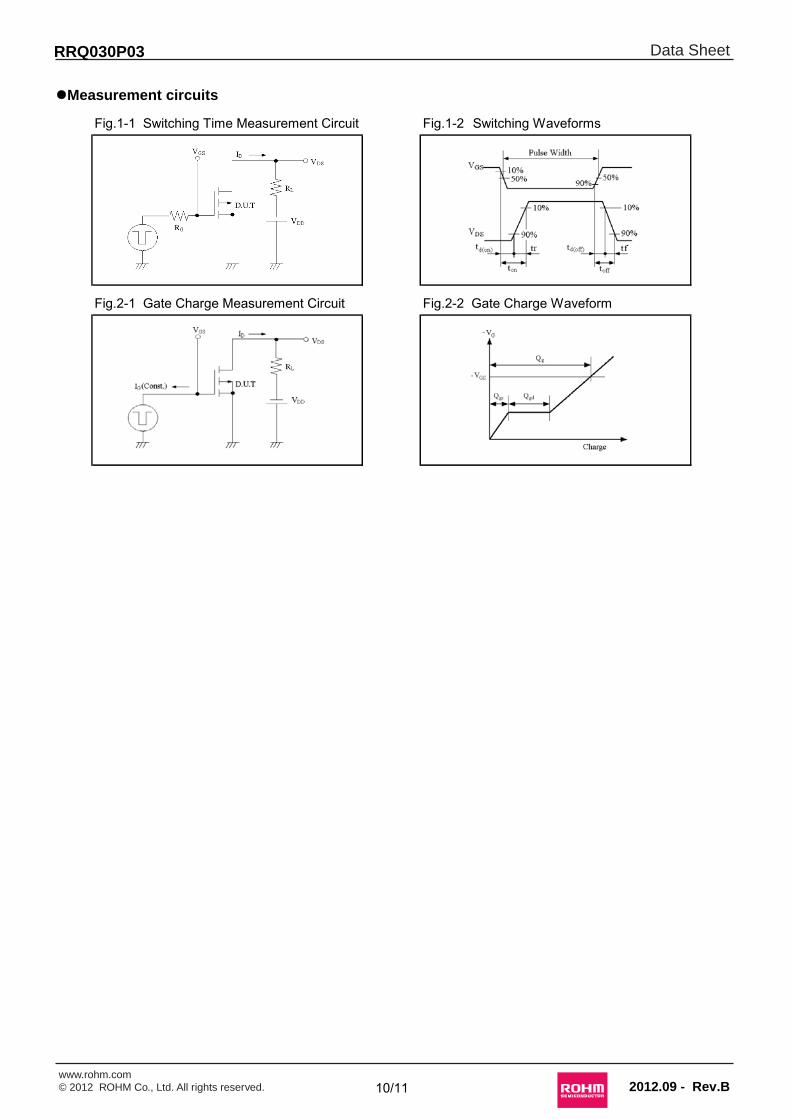
lMeasurement circuits
Fig.1-1 Switching Time Measurement Circuit Fig.1-2 Switching Waveforms
Fig.2-1 Gate Charge Measurement Circuit Fig.2-2 Gate Charge Waveform
10/11 2012.09 - Rev.B
www.rohm.com© 2012 ROHM Co., Ltd. All rights reserved.
Data SheetRRQ030P03
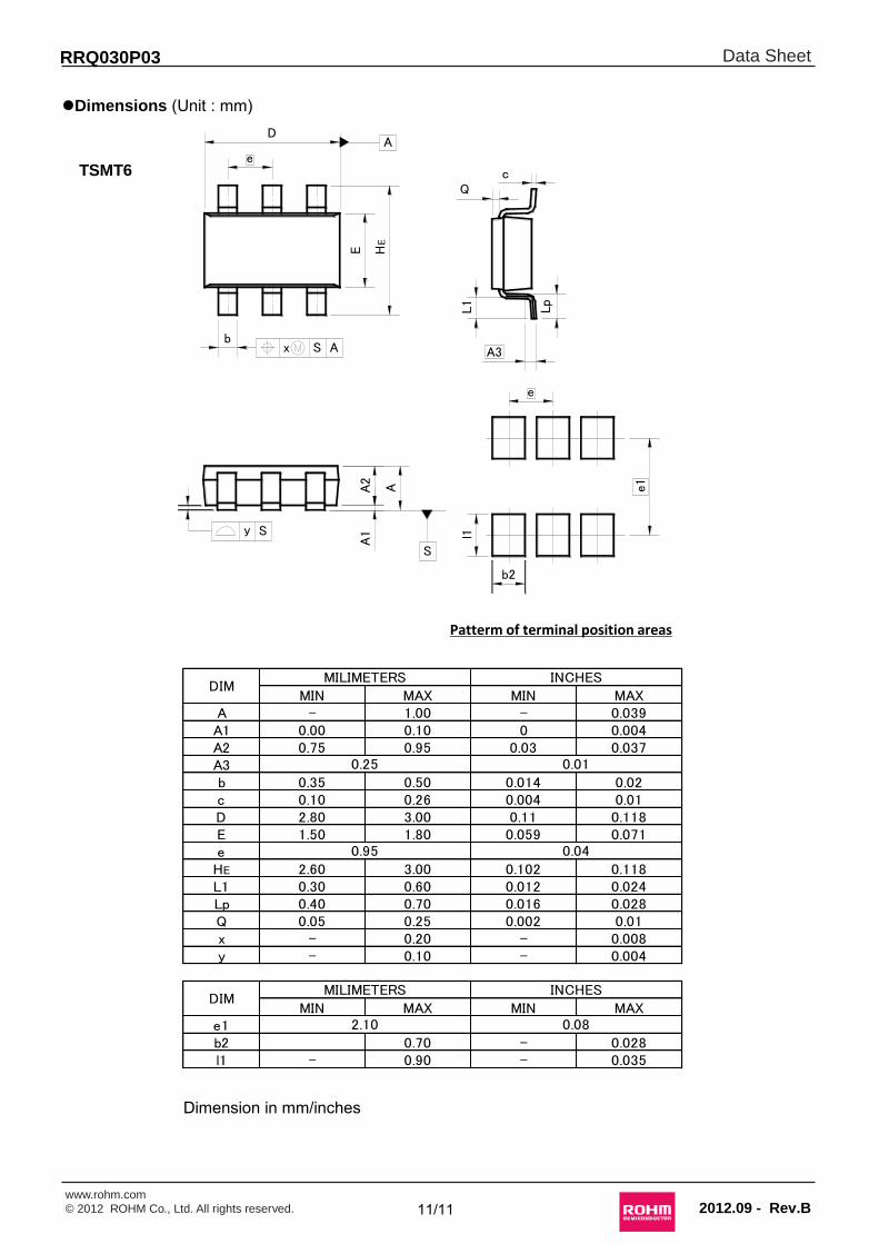
lDimensions (Unit : mm)
Dimension in mm/inches
TSMT6
Patterm of terminal position areas
e
D
E H
b
E
Lp
L1
A3
c
A
x S A
A1
A2
S
y S
A e1
e
b2
l1
Q
MIN MAX MIN MAXA - 1.00 - 0.039A1 0.00 0.10 0 0.004A2 0.75 0.95 0.03 0.037A3b 0.35 0.50 0.014 0.02c 0.10 0.26 0.004 0.01D 2.80 3.00 0.11 0.118E 1.50 1.80 0.059 0.071eHE 2.60 3.00 0.102 0.118L1 0.30 0.60 0.012 0.024Lp 0.40 0.70 0.016 0.028Q 0.05 0.25 0.002 0.01x - 0.20 - 0.008y - 0.10 - 0.004
MIN MAX MIN MAXe1b2 0.70 - 0.028l1 - 0.90 - 0.035
0.25 0.01
DIMMILIMETERS INCHES
2.10 0.08
DIMMILIMETERS INCHES
0.95 0.04
11/11 2012.09 - Rev.B

R1120Awww.rohm.com© 2012 ROHM Co., Ltd. All rights reserved.
Notice
ROHM Customer Support System http://www.rohm.com/contact/
Thank you for your accessing to ROHM product informations. More detail product informations and catalogs are available, please contact us.
N o t e s
No copying or reproduction of this document, in part or in whole, is permitted without the consent of ROHM Co.,Ltd. The content specified herein is subject to change for improvement without notice. The content specified herein is for the purpose of introducing ROHM's products (hereinafter "Products"). If you wish to use any such Product, please be sure to refer to the specifications, which can be obtained from ROHM upon request. Examples of application circuits, circuit constants and any other information contained herein illustrate the standard usage and operations of the Products. The peripheral conditions must be taken into account when designing circuits for mass production. Great care was taken in ensuring the accuracy of the information specified in this document. However, should you incur any damage arising from any inaccuracy or misprint of such information, ROHM shall bear no responsibility for such damage. The technical information specified herein is intended only to show the typical functions of and examples of application circuits for the Products. ROHM does not grant you, explicitly or implicitly, any license to use or exercise intellectual property or other rights held by ROHM and other parties. ROHM shall bear no responsibility whatsoever for any dispute arising from the use of such technical information. The Products specified in this document are intended to be used with general-use electronic equipment or devices (such as audio visual equipment, office-automation equipment, commu-nication devices, electronic appliances and amusement devices). The Products specified in this document are not designed to be radiation tolerant. While ROHM always makes efforts to enhance the quality and reliability of its Products, a Product may fail or malfunction for a variety of reasons. Please be sure to implement in your equipment using the Products safety measures to guard against the possibility of physical injury, fire or any other damage caused in the event of the failure of any Product, such as derating, redundancy, fire control and fail-safe designs. ROHM shall bear no responsibility whatsoever for your use of any Product outside of the prescribed scope or not in accordance with the instruction manual. The Products are not designed or manufactured to be used with any equipment, device or system which requires an extremely high level of reliability the failure or malfunction of which may result in a direct threat to human life or create a risk of human injury (such as a medical instrument, transportation equipment, aerospace machinery, nuclear-reactor controller, fuel-controller or other safety device). ROHM shall bear no responsibility in any way for use of any of the Products for the above special purposes. If a Product is intended to be used for any such special purpose, please contact a ROHM sales representative before purchasing. If you intend to export or ship overseas any Product or technology specified herein that may be controlled under the Foreign Exchange and the Foreign Trade Law, you will be required to obtain a license or permit under the Law.


![Panasonic Sc-Ak970lb-k Br [ET]](https://static.fdocument.org/doc/165x107/55cf944e550346f57ba11646/panasonic-sc-ak970lb-k-br-et.jpg)