TP2271 TP2272 3 P E A K 8-Pin SOIC 8-Pin … · TP2271/ / 3 TP2272 TP2274 36V Single supply, 7MHz...
16
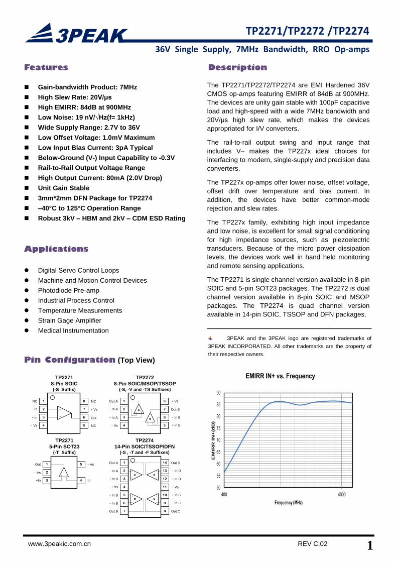
3PEAK 1 TP2271/TP2272 /TP2274 36V Single Supply, 7MHz Bandwidth, RRO Op-amps www.3peakic.com.cn REV C.02 Features Gain-bandwidth Product: 7MHz High Slew Rate: 20V/μs High EMIRR: 84dB at 900MHz Low Noise: 19 nV/√Hz(f= 1kHz) Wide Supply Range: 2.7V to 36V Low Offset Voltage: 1.0mV Maximum Low Input Bias Current: 3pA Typical Below-Ground (V-) Input Capability to -0.3V Rail-to-Rail Output Voltage Range High Output Current: 80mA (2.0V Drop) Unit Gain Stable 3mm*2mm DFN Package for TP2274 –40°C to 125°C Operation Range Robust 3kV – HBM and 2kV – CDM ESD Rating Applications Digital Servo Control Loops Machine and Motion Control Devices Photodiode Pre-amp Industrial Process Control Temperature Measurements Strain Gage Amplifier Medical Instrumentation Pin Configuration (Top View) TP2272 8-Pin SOIC/MSOP/TSSOP (-S, -V and -TS Suffixes) 8 6 5 7 3 2 1 4 Out A ﹢In A ﹣In A ﹢In B ﹣In B Out B A B ﹣Vs ﹢Vs TP2274 14-Pin SOIC/TSSOP/DFN (-S , -T and -F Suffixes) 14 13 12 11 10 9 8 6 5 7 3 2 1 4 Out A ﹢In A ﹣In A D A C B Out D ﹢In D ﹣In D Out B ﹢In B ﹣In B Out C ﹢In C ﹣In C ﹣Vs ﹢Vs TP2271 8-Pin SOIC (-S Suffix) Out TP2271 5-Pin SOT23 (-T Suffix) 8 6 5 7 3 2 1 4 NC ﹢In ﹣In ﹣Vs ﹢Vs NC NC 4 5 3 2 1 Out +In -In ﹣Vs ﹢Vs Description The TP2271/TP2272/TP2274 are EMI Hardened 36V CMOS op-amps featuring EMIRR of 84dB at 900MHz. The devices are unity gain stable with 100pF capacitive load and high-speed with a wide 7MHz bandwidth and 20V/μs high slew rate, which makes the devices appropriated for I/V converters. The rail-to-rail output swing and input range that includes V– makes the TP227x ideal choices for interfacing to modern, single-supply and precision data converters. The TP227x op-amps offer lower noise, offset voltage, offset drift over temperature and bias current. In addition, the devices have better common-mode rejection and slew rates. The TP227x family, exhibiting high input impedance and low noise, is excellent for small signal conditioning for high impedance sources, such as piezoelectric transducers. Because of the micro power dissipation levels, the devices work well in hand held monitoring and remote sensing applications. The TP2271 is single channel version available in 8-pin SOIC and 5-pin SOT23 packages. The TP2272 is dual channel version available in 8-pin SOIC and MSOP packages. The TP2274 is quad channel version available in 14-pin SOIC, TSSOP and DFN packages. 3PEAK and the 3PEAK logo are registered trademarks of 3PEAK INCORPORATED. All other trademarks are the property of their respective owners. EMIRR IN+ vs. Frequency 50 55 60 65 70 75 80 85 90 400 4000 EMIRR IN+(dB) Frequency (MHz)
Transcript of TP2271 TP2272 3 P E A K 8-Pin SOIC 8-Pin … · TP2271/ / 3 TP2272 TP2274 36V Single supply, 7MHz...
3PEAK
1
TP2271/TP2272 /TP2274
36V Single Supply, 7MHz Bandwidth, RRO Op-amps
www.3peakic.com.cn REV C.02
Features
Gain-bandwidth Product: 7MHz
High Slew Rate: 20V/μs
High EMIRR: 84dB at 900MHz
Low Noise: 19 nV/√Hz(f= 1kHz)
Wide Supply Range: 2.7V to 36V
Low Offset Voltage: 1.0mV Maximum
Low Input Bias Current: 3pA Typical
Below-Ground (V-) Input Capability to -0.3V
Rail-to-Rail Output Voltage Range
High Output Current: 80mA (2.0V Drop)
Unit Gain Stable
3mm*2mm DFN Package for TP2274
–40°C to 125°C Operation Range
Robust 3kV – HBM and 2kV – CDM ESD Rating
Applications
Digital Servo Control Loops
Machine and Motion Control Devices
Photodiode Pre-amp
Industrial Process Control
Temperature Measurements
Strain Gage Amplifier
Medical Instrumentation
Pin Configuration (Top View)
TP2272
8-Pin SOIC/MSOP/TSSOP(-S, -V and -TS Suffixes)
8
6
5
7
3
2
1
4
Out A
﹢In A
﹣In A
﹢In B
﹣In B
Out BA
B
﹣Vs
﹢Vs
TP2274
14-Pin SOIC/TSSOP/DFN(-S , -T and -F Suffixes)
14
13
12
11
10
9
8
6
5
7
3
2
1
4
Out A
﹢In A
﹣In ADA
CB
Out D
﹢In D
﹣In D
Out B
﹢In B
﹣In B
Out C
﹢In C
﹣In C
﹣Vs﹢Vs
TP2271
8-Pin SOIC(-S Suffix)
Out
TP2271
5-Pin SOT23(-T Suffix)
8
6
5
7
3
2
1
4
NC
﹢In
﹣In
﹣Vs
﹢Vs
NC
NC
4
5
3
2
1Out
+In -In
﹣Vs
﹢Vs
Description
The TP2271/TP2272/TP2274 are EMI Hardened 36V
CMOS op-amps featuring EMIRR of 84dB at 900MHz.
The devices are unity gain stable with 100pF capacitive
load and high-speed with a wide 7MHz bandwidth and
20V/μs high slew rate, which makes the devices
appropriated for I/V converters.
The rail-to-rail output swing and input range that
includes V– makes the TP227x ideal choices for
interfacing to modern, single-supply and precision data
converters.
The TP227x op-amps offer lower noise, offset voltage,
offset drift over temperature and bias current. In
addition, the devices have better common-mode
rejection and slew rates.
The TP227x family, exhibiting high input impedance
and low noise, is excellent for small signal conditioning
for high impedance sources, such as piezoelectric
transducers. Because of the micro power dissipation
levels, the devices work well in hand held monitoring
and remote sensing applications.
The TP2271 is single channel version available in 8-pin
SOIC and 5-pin SOT23 packages. The TP2272 is dual
channel version available in 8-pin SOIC and MSOP
packages. The TP2274 is quad channel version
available in 14-pin SOIC, TSSOP and DFN packages.
3PEAK and the 3PEAK logo are registered trademarks of
3PEAK INCORPORATED. All other trademarks are the property of
their respective owners.
EMIRR IN+ vs. Frequency
50
55
60
65
70
75
80
85
90
400 4000
EM
IRR
IN
+(d
B)
Frequency (MHz)
2 REV C.02
www.3peakic.com.cn
TP2271 / TP2272 / TP2274
36V Single supply, 7MHz Bandwidth, RRO Op-amps
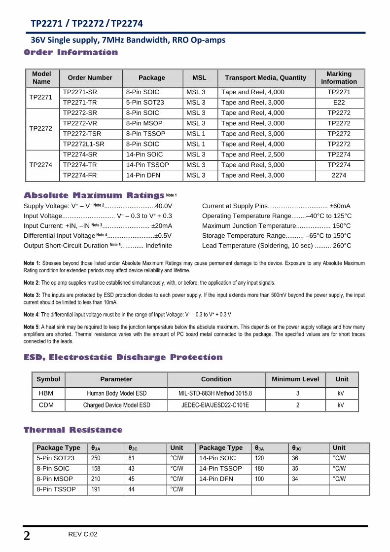
Order Information
Model
Name Order Number Package MSL Transport Media, Quantity
Marking
Information
TP2271 TP2271-SR 8-Pin SOIC MSL 3 Tape and Reel, 4,000 TP2271
TP2271-TR 5-Pin SOT23 MSL 3 Tape and Reel, 3,000 E22
TP2272
TP2272-SR 8-Pin SOIC MSL 3 Tape and Reel, 4,000 TP2272
TP2272-VR 8-Pin MSOP MSL 3 Tape and Reel, 3,000 TP2272
TP2272-TSR 8-Pin TSSOP MSL 1 Tape and Reel, 3,000 TP2272
TP2272L1-SR 8-Pin SOIC MSL 1 Tape and Reel, 4,000 TP2272
TP2274
TP2274-SR 14-Pin SOIC MSL 3 Tape and Reel, 2,500 TP2274
TP2274-TR 14-Pin TSSOP MSL 3 Tape and Reel, 3,000 TP2274
TP2274-FR 14-Pin DFN MSL 3 Tape and Reel, 3,000 2274
Absolute Maximum Ratings Note 1
Supply Voltage: V+ – V– Note 2............................40.0V
Input Voltage............................. V– – 0.3 to V+ + 0.3
Input Current: +IN, –IN Note 3.......................... ±20mA
Differential Input Voltage Note 4..........................±0.5V
Output Short-Circuit Duration Note 5…......... Indefinite
Current at Supply Pins……………............... ±60mA
Operating Temperature Range........–40°C to 125°C
Maximum Junction Temperature................... 150°C
Storage Temperature Range.......... –65°C to 150°C
Lead Temperature (Soldering, 10 sec) ......... 260°C
Note 1: Stresses beyond those listed under Absolute Maximum Ratings may cause permanent damage to the device. Exposure to any Absolute Maximum
Rating condition for extended periods may affect device reliability and lifetime.
Note 2: The op amp supplies must be established simultaneously, with, or before, the application of any input signals.
Note 3: The inputs are protected by ESD protection diodes to each power supply. If the input extends more than 500mV beyond the power supply, the input
current should be limited to less than 10mA.
Note 4: The differential input voltage must be in the range of Input Voltage: V– – 0.3 to V+ + 0.3 V
Note 5: A heat sink may be required to keep the junction temperature below the absolute maximum. This depends on the power supply voltage and how many
amplifiers are shorted. Thermal resistance varies with the amount of PC board metal connected to the package. The specified values are for short traces
connected to the leads.
ESD, Electrostatic Discharge Protection
Symbol Parameter Condition Minimum Level Unit
HBM Human Body Model ESD MIL-STD-883H Method 3015.8 3 kV
CDM Charged Device Model ESD JEDEC-EIA/JESD22-C101E 2 kV
Thermal Resistance
Package Type θJA θJC Unit Package Type θJA θJC Unit
5-Pin SOT23 250 81 ° C/W 14-Pin SOIC 120 36 ° C/W
8-Pin SOIC 158 43 ° C/W 14-Pin TSSOP 180 35 ° C/W
8-Pin MSOP 210 45 ° C/W 14-Pin DFN 100 34 ° C/W
8-Pin TSSOP 191 44 ° C/W
3
TP2271/TP2272 / TP2274
36V Single supply, 7MHz Bandwidth, RRO Op-amps
www.3peakic.com.cn REV C.02
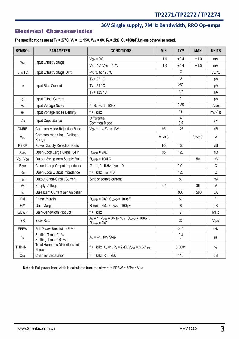
Electrical Characteristics
The specifications are at TA = 27° C. VS = ±15V, VCM = 0V, RL = 2kΩ, CL =100pF.Unless otherwise noted.
SYMBOL PARAMETER CONDITIONS MIN TYP MAX UNITS
VOS Input Offset Voltage VCM = 0V -1.0 ± 0.4 +1.0 mV
VS = 5V, VCM = 2.5V -1.0 ± 0.4 +1.0 mV
VOS TC Input Offset Voltage Drift -40° C to 125° C 2 μV/° C
IB Input Bias Current
TA = 27 ° C 3 pA
TA = 85 ° C 250 pA
TA = 125 ° C 7.7 nA
IOS Input Offset Current 1 pA
Vn Input Voltage Noise f = 0.1Hz to 10Hz 2.35 μVRMS
en Input Voltage Noise Density f = 1kHz 19 nV/√Hz
CIN Input Capacitance Differential
Common Mode
4
2.5 pF
CMRR Common Mode Rejection Ratio VCM = -14.5V to 13V 95 126 dB
VCM Common-mode Input Voltage
Range V– -0.3 V+-2.0 V
PSRR Power Supply Rejection Ratio 95 130 dB
AVOL Open-Loop Large Signal Gain RLOAD = 2kΩ 95 120 dB
VOL, VOH Output Swing from Supply Rail RLOAD = 100kΩ 50 mV
ROUT Closed-Loop Output Impedance G = 1, f =1kHz, IOUT = 0 0.01 Ω
RO Open-Loop Output Impedance f = 1kHz, IOUT = 0 125 Ω
ISC Output Short-Circuit Current Sink or source current 80 mA
VS Supply Voltage 2.7 36 V
IQ Quiescent Current per Amplifier 900 1500 μA
PM Phase Margin RLOAD = 2kΩ, CLOAD = 100pF 60 °
GM Gain Margin RLOAD = 2kΩ, CLOAD = 100pF 8 dB
GBWP Gain-Bandwidth Product f = 1kHz 7 MHz
SR Slew Rate AV = 1, VOUT = 0V to 10V, CLOAD = 100pF,
RLOAD = 2kΩ 20 V/μs
FPBW Full Power Bandwidth Note 1 210 kHz
tS Settling Time, 0.1%
Settling Time, 0.01% AV = –1, 10V Step
0.8
1 μs
THD+N Total Harmonic Distortion and
Noise f = 1kHz, AV =1, RL = 2kΩ, VOUT = 3.5VRMS 0.0001 %
Xtalk Channel Separation f = 1kHz, RL = 2kΩ 110 dB
Note 1: Full power bandwidth is calculated from the slew rate FPBW = SR/π • VP-P
4 REV C.02
www.3peakic.com.cn
TP2271 / TP2272 / TP2274
36V Single supply, 7MHz Bandwidth, RRO Op-amps
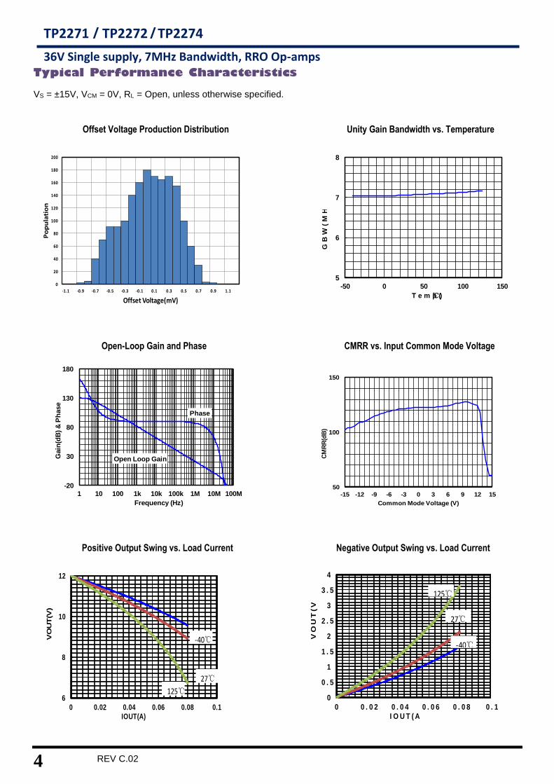
Typical Performance Characteristics
VS = ±15V, VCM = 0V, RL = Open, unless otherwise specified.
Offset Voltage Production Distribution Unity Gain Bandwidth vs. Temperature
0
20
40
60
80
100
120
140
160
180
200
-1.1 -0.9 -0.7 -0.5 -0.3 -0.1 0.1 0.3 0.5 0.7 0.9 1.1
Po
pu
lati
on
Offset Voltage(mV)
5
6
7
8
-50 0 50 100 150
GB
W(
MH
z)
T e m p (℃)
Open-Loop Gain and Phase CMRR vs. Input Common Mode Voltage
-20
30
80
130
180
1 10 100 1k 10k 100k 1M 10M 100M
Gain
(dB
) &
Ph
ase
Frequency (Hz)
Phase
Open Loop Gain
50
100
150
-15 -12 -9 -6 -3 0 3 6 9 12 15
CM
RR
(dB
)
Common Mode Voltage (V)
Positive Output Swing vs. Load Current Negative Output Swing vs. Load Current
6
8
10
12
0 0.02 0.04 0.06 0.08 0.1
VO
UT
(V)
IOUT(A)
125℃
27℃
-40℃
0
0 . 5
1
1 . 5
2
2 . 5
3
3 . 5
4
0 0 . 0 2 0 . 0 4 0 . 0 6 0 . 0 8 0 . 1
VO
UT
(V
)
I O U T ( A )
125℃
27℃
-40℃
5
TP2271/TP2272 / TP2274
36V Single supply, 7MHz Bandwidth, RRO Op-amps
www.3peakic.com.cn REV C.02
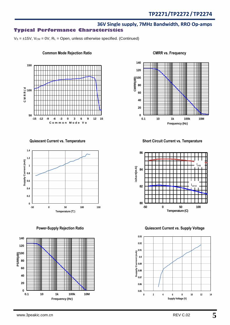
Typical Performance Characteristics
VS = ±15V, VCM = 0V, RL = Open, unless otherwise specified. (Continued)
Common Mode Rejection Ratio CMRR vs. Frequency
50
100
150
-15 -12 -9 -6 -3 0 3 6 9 12 15
CM
RR
(d
B)
C o m m o n M o d e V o l t a g e ( V )
0
20
40
60
80
100
120
140
0.1 10 1k 100k 10M
CM
RR
(dB
)
Frequency (Hz)
Quiescent Current vs. Temperature Short Circuit Current vs. Temperature
0
0.2
0.4
0.6
0.8
1
1.2
1.4
-50 0 50 100 150
Su
pp
ly C
urr
en
t (m
A)
Temperature (℃)
80
82
84
86
-50 0 50 100
ish
ort
(mA
)
Temperature (C)
Isorce
Isink
Power-Supply Rejection Ratio Quiescent Current vs. Supply Voltage
0
20
40
60
80
100
120
140
0.1 10 1k 100k 10M
PS
RR
(dB
)
Frequency (Hz)
0.85
0.86
0.87
0.88
0.89
0.9
0.91
0.92
0.93
0 2 4 6 8 10 12 14
Su
pp
ly C
urre
nt
(mA
)
Supply Voltage (V)
6 REV C.02
www.3peakic.com.cn
TP2271 / TP2272 / TP2274
36V Single supply, 7MHz Bandwidth, RRO Op-amps
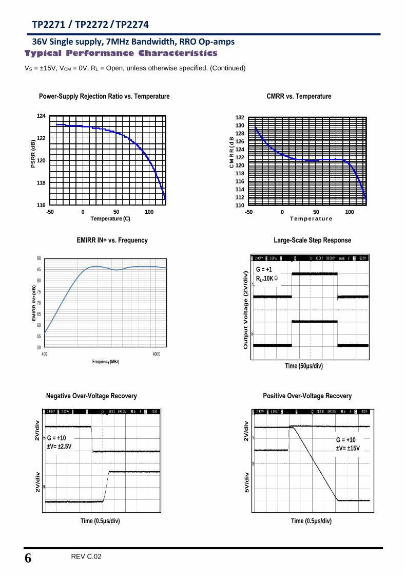
Typical Performance Characteristics
VS = ±15V, VCM = 0V, RL = Open, unless otherwise specified. (Continued)
Power-Supply Rejection Ratio vs. Temperature CMRR vs. Temperature
116
118
120
122
124
-50 0 50 100
PS
RR
(d
B)
Temperature (C)
110
112
114
116
118
120
122
124
126
128
130
132
-50 0 50 100
CM
RR
(d
B)
T em p er atu r e (C)
EMIRR IN+ vs. Frequency Large-Scale Step Response
50
55
60
65
70
75
80
85
90
400 4000
EM
IRR
IN
+(d
B)
Frequency (MHz)
Time (50μs/div)
Ou
tpu
t V
olt
ag
e (
2V
/div
) G = +1
RL=10KΩ
Negative Over-Voltage Recovery Positive Over-Voltage Recovery
G = +1
RL=10KΩ
2V
/div
Time (0.5μs/div)
2V
/div
G = +10
±V= ±2.5V
2V
/div
Time (0.5μs/div)
5V
/div
G = +10
±V= ±15V
7
TP2271/TP2272 / TP2274
36V Single supply, 7MHz Bandwidth, RRO Op-amps
www.3peakic.com.cn REV C.02
Pin Functions
-IN: Inverting Input of the Amplifier. Voltage range of this
pin can go from V– to (V+ - 2.0V).
+IN: Non-Inverting Input of Amplifier. This pin has the
same voltage range as –IN.
V+ or +VS: Positive Power Supply. Typically the voltage
is from 2.7V to 36V. Split supplies are possible as long
as the voltage between V+ and V– is between 2.7V and
36V. A bypass capacitor of 0.1μF as close to the part as
possible should be used between power supply pins or
between supply pins and ground.
V– or –VS: Negative Power Supply. It is normally tied to
ground. It can also be tied to a voltage other than
ground as long as the voltage between V+ and V– is from
2.7V to 36V. If it is not connected to ground, bypass it
with a capacitor of 0.1μF as close to the part as
possible.
OUT: Amplifier Output. The voltage range extends to
within milli-volts of each supply rail.
N/C: No connection.
The exposed thermal pad of DFN package should be
left floated.
Operation
The TP227x op-amps have input signal range from V– to (V+ – 2.0V). The output can extend all the way to the supply
rails. The input stage is comprised of a PMOS differential amplifier. The Class-AB control buffer and output bias stage
uses a proprietary compensation technique to take full advantage of the process technology to drive very high
capacitive loads. This is evident from the transient over shoot measurement plots in the Typical Performance
Characteristics.
Applications Information
EMI Harden
The EMI hardening makes the TP2271/2272/2274 a must for almost all op amp applications. Most applications are
exposed to Radio Frequency (RF) signals such as the signals transmitted by mobile phones or wireless computer
peripherals. The TP2271/2272/2274 will effectively reduce disturbances caused by RF signals to a level that will be
hardly noticeable. This again reduces the need for additional filtering and shielding Using this EMI resistant series of
op amps will thus reduce the number of components and space needed for applications that are affected by EMI, and
will help applications, not yet identified as possible EMI sensitive, to be more robust for EMI.
Wide Supply Voltage
The TP2271/2272/2274 operational amplifiers can operate with power supply voltages from 2.7V to 36V. Each
amplifier draws 0.8mA quiescent current at 36V supply voltage. The TP2271/2272/2274 is optimized for wide
bandwidth low power applications. They have an industry leading high GBW to power ratio and the GBW remains
nearly constant over specified temperature range.
Low Input Bias Current
The TP2271/2272/2274 is a CMOS OPA family and features very low input bias current in pA range. The low input
bias current allows the amplifiers to be used in applications with high resistance sources. Care must be taken to
minimize PCB Surface Leakage. See below section on “PCB Surface Leakage” for more details.
PCB Surface Leakage
In applications where low input bias current is critical, Printed Circuit Board (PCB) surface leakage effects need to be
considered. Surface leakage is caused by humidity, dust or other contamination on the board. Under low humidity
conditions, a typical resistance between nearby traces is 1012Ω. A 5V difference would cause 5pA of current to flow,
8 REV C.02
www.3peakic.com.cn
TP2271 / TP2272 / TP2274
36V Single supply, 7MHz Bandwidth, RRO Op-amps
which is greater than the TP2271/2272/2274 OPA’s input bias current at +27°C (±3pA, typical). It is recommended to
use multi-layer PCB layout and route the OPA’s -IN and +IN signal under the PCB surface.
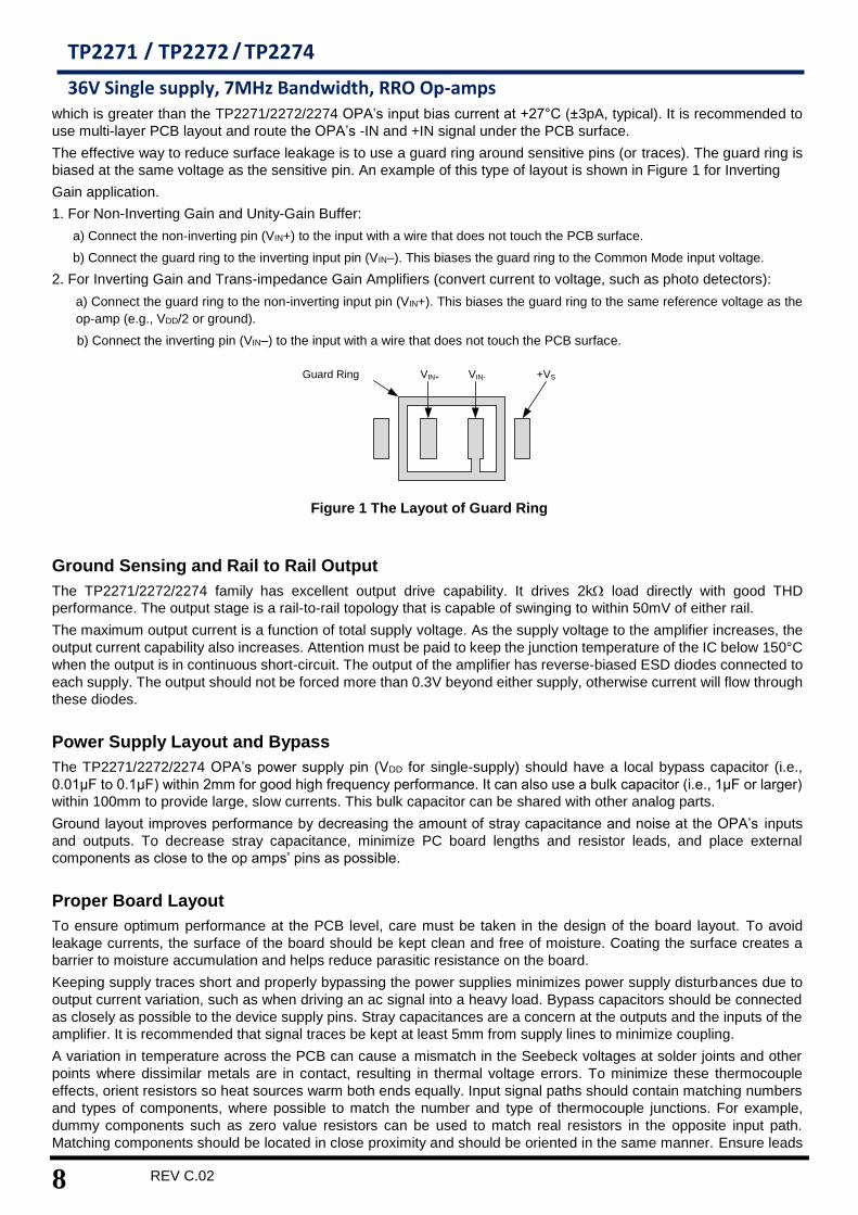
The effective way to reduce surface leakage is to use a guard ring around sensitive pins (or traces). The guard ring is
biased at the same voltage as the sensitive pin. An example of this type of layout is shown in Figure 1 for Inverting
Gain application.
1. For Non-Inverting Gain and Unity-Gain Buffer:
a) Connect the non-inverting pin (VIN+) to the input with a wire that does not touch the PCB surface.
b) Connect the guard ring to the inverting input pin (VIN–). This biases the guard ring to the Common Mode input voltage.
2. For Inverting Gain and Trans-impedance Gain Amplifiers (convert current to voltage, such as photo detectors):
a) Connect the guard ring to the non-inverting input pin (VIN+). This biases the guard ring to the same reference voltage as the
op-amp (e.g., VDD/2 or ground).
b) Connect the inverting pin (VIN–) to the input with a wire that does not touch the PCB surface.
VIN+ VIN- +VSGuard Ring
Figure 1 The Layout of Guard Ring
Ground Sensing and Rail to Rail Output
The TP2271/2272/2274 family has excellent output drive capability. It drives 2k load directly with good THD
performance. The output stage is a rail-to-rail topology that is capable of swinging to within 50mV of either rail.
The maximum output current is a function of total supply voltage. As the supply voltage to the amplifier increases, the
output current capability also increases. Attention must be paid to keep the junction temperature of the IC below 150°C
when the output is in continuous short-circuit. The output of the amplifier has reverse-biased ESD diodes connected to
each supply. The output should not be forced more than 0.3V beyond either supply, otherwise current will flow through
these diodes.
Power Supply Layout and Bypass
The TP2271/2272/2274 OPA’s power supply pin (VDD for single-supply) should have a local bypass capacitor (i.e.,
0.01μF to 0.1μF) within 2mm for good high frequency performance. It can also use a bulk capacitor (i.e., 1μF or larger)
within 100mm to provide large, slow currents. This bulk capacitor can be shared with other analog parts.
Ground layout improves performance by decreasing the amount of stray capacitance and noise at the OPA’s inputs
and outputs. To decrease stray capacitance, minimize PC board lengths and resistor leads, and place external
components as close to the op amps’ pins as possible.
Proper Board Layout
To ensure optimum performance at the PCB level, care must be taken in the design of the board layout. To avoid
leakage currents, the surface of the board should be kept clean and free of moisture. Coating the surface creates a
barrier to moisture accumulation and helps reduce parasitic resistance on the board.
Keeping supply traces short and properly bypassing the power supplies minimizes power supply disturbances due to
output current variation, such as when driving an ac signal into a heavy load. Bypass capacitors should be connected
as closely as possible to the device supply pins. Stray capacitances are a concern at the outputs and the inputs of the
amplifier. It is recommended that signal traces be kept at least 5mm from supply lines to minimize coupling.
A variation in temperature across the PCB can cause a mismatch in the Seebeck voltages at solder joints and other
points where dissimilar metals are in contact, resulting in thermal voltage errors. To minimize these thermocouple
effects, orient resistors so heat sources warm both ends equally. Input signal paths should contain matching numbers
and types of components, where possible to match the number and type of thermocouple junctions. For example,
dummy components such as zero value resistors can be used to match real resistors in the opposite input path.
Matching components should be located in close proximity and should be oriented in the same manner. Ensure leads
9
TP2271/TP2272 / TP2274
36V Single supply, 7MHz Bandwidth, RRO Op-amps
www.3peakic.com.cn REV C.02
are of equal length so that thermal conduction is in equilibrium. Keep heat sources on the PCB as far away from
amplifier input circuitry as is practical.
The use of a ground plane is highly recommended. A ground plane reduces EMI noise and also helps to maintain a
constant temperature across the circuit board.
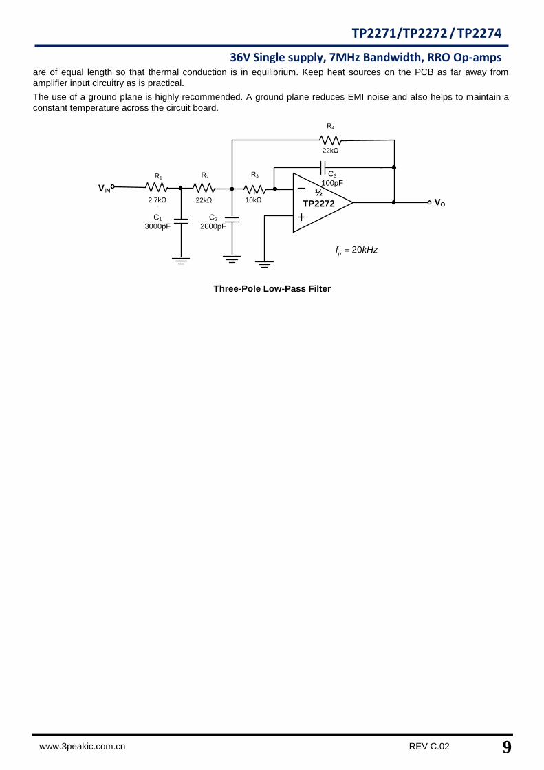
½
TP2272
VIN
C1
3000pF
R2
22kΩ
22kΩ
R4
R1
2.7kΩ 10kΩ
R3 C3
100pF
VO
C2
2000pF
20pf kHz
Three-Pole Low-Pass Filter
10 REV C.02
www.3peakic.com.cn
TP2271 / TP2272 / TP2274
36V Single supply, 7MHz Bandwidth, RRO Op-amps
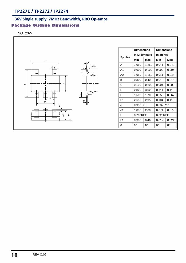
Package Outline Dimensions
SOT23-5
Symbol
Dimensions
In Millimeters
Dimensions
In Inches
Min Max Min Max
A 1.050 1.250 0.041 0.049
A1 0.000 0.100 0.000 0.004
A2 1.050 1.150 0.041 0.045
b 0.300 0.400 0.012 0.016
C 0.100 0.200 0.004 0.008
D 2.820 3.020 0.111 0.119
E 1.500 1.700 0.059 0.067
E1 2.650 2.950 0.104 0.116
e 0.950TYP 0.037TYP
e1 1.800 2.000 0.071 0.079
L 0.700REF 0.028REF
L1 0.300 0.460 0.012 0.024
θ 0° 8° 0° 8°
11
TP2271/TP2272 / TP2274
36V Single supply, 7MHz Bandwidth, RRO Op-amps
www.3peakic.com.cn REV C.02
D
E1
b
E
A1
A2
e
θ
L1
C
Package Outline Dimensions
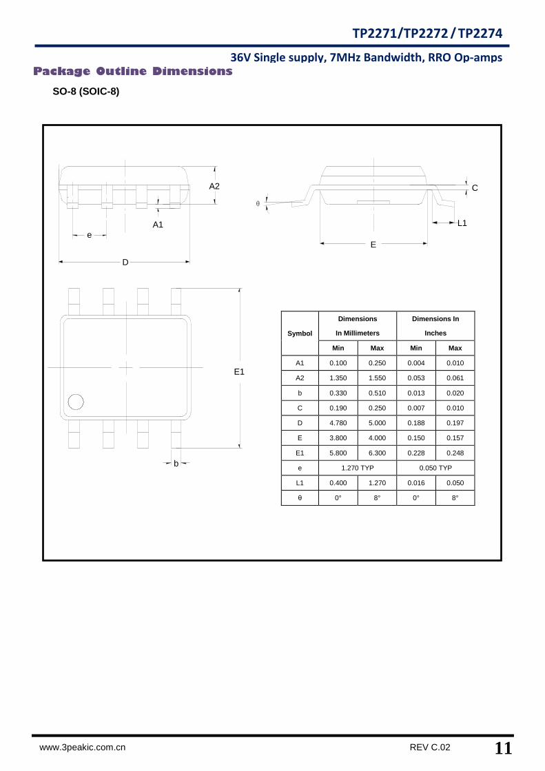
SO-8 (SOIC-8)
Symbol
Dimensions
In Millimeters
Dimensions In
Inches
Min Max Min Max
A1 0.100 0.250 0.004 0.010
A2 1.350 1.550 0.053 0.061
b 0.330 0.510 0.013 0.020
C 0.190 0.250 0.007 0.010
D 4.780 5.000 0.188 0.197
E 3.800 4.000 0.150 0.157
E1 5.800 6.300 0.228 0.248
e 1.270 TYP 0.050 TYP
L1 0.400 1.270 0.016 0.050
θ 0° 8° 0° 8°
12 REV C.02
www.3peakic.com.cn
TP2271 / TP2272 / TP2274
36V Single supply, 7MHz Bandwidth, RRO Op-amps
Package Outline Dimensions
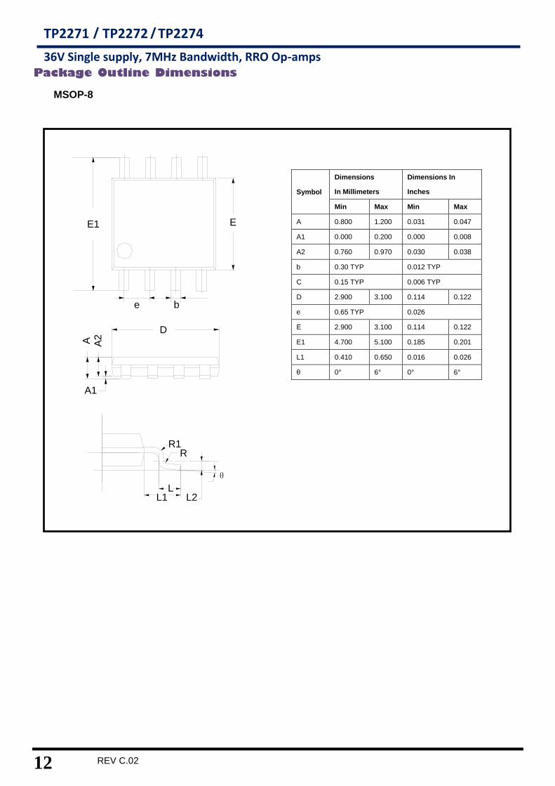
MSOP-8
Symbol
Dimensions
In Millimeters
Dimensions In
Inches
Min Max Min Max
A 0.800 1.200 0.031 0.047
A1 0.000 0.200 0.000 0.008
A2 0.760 0.970 0.030 0.038
b 0.30 TYP 0.012 TYP
C 0.15 TYP 0.006 TYP
D 2.900 3.100 0.114 0.122
e 0.65 TYP 0.026
E 2.900 3.100 0.114 0.122
E1 4.700 5.100 0.185 0.201
L1 0.410 0.650 0.016 0.026
θ 0° 6° 0° 6°
E1
e
E
A1
A2A
D
L1 L2L
RR1
θ
b
13
TP2271/TP2272 / TP2274
36V Single supply, 7MHz Bandwidth, RRO Op-amps
www.3peakic.com.cn REV C.02
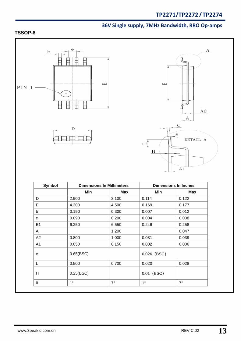
TSSOP-8
Symbol Dimensions In Millimeters Dimensions In Inches
Min Max Min Max
D 2.900 3.100 0.114 0.122
E 4.300 4.500 0.169 0.177
b 0.190 0.300 0.007 0.012
c 0.090 0.200 0.004 0.008
E1 6.250 6.550 0.246 0.258
A 1.200 0.047
A2 0.800 1.000 0.031 0.039
A1 0.050 0.150 0.002 0.006
e 0.65(BSC) 0.026(BSC)
L 0.500 0.700 0.020 0.028
H 0.25(BSC) 0.01(BSC)
θ 1° 7° 1° 7°
14 REV C.02
www.3peakic.com.cn
TP2271 / TP2272 / TP2274
36V Single supply, 7MHz Bandwidth, RRO Op-amps
Package Outline Dimensions
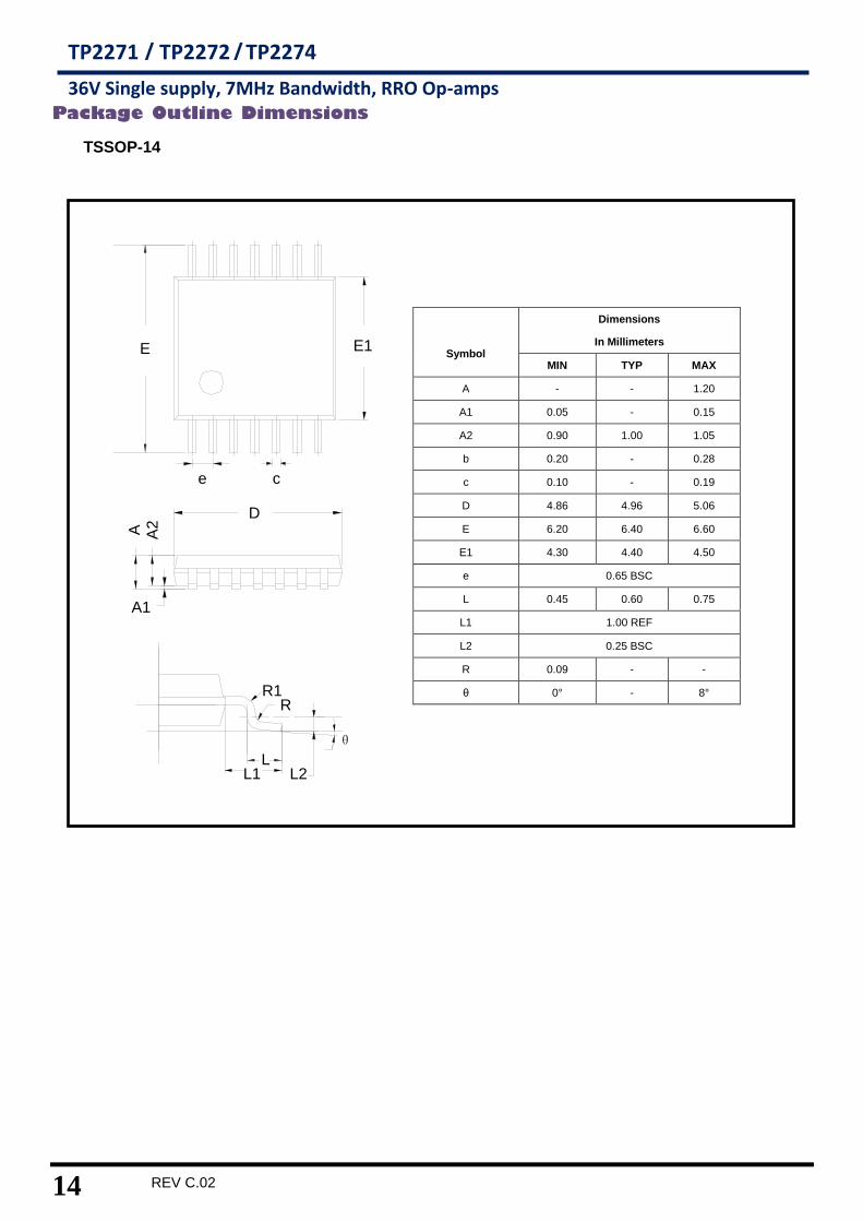
TSSOP-14
Symbol
Dimensions
In Millimeters
MIN TYP MAX
A - - 1.20
A1 0.05 - 0.15
A2 0.90 1.00 1.05
b 0.20 - 0.28
c 0.10 - 0.19
D 4.86 4.96 5.06
E 6.20 6.40 6.60
E1 4.30 4.40 4.50
e 0.65 BSC
L 0.45 0.60 0.75
L1 1.00 REF
L2 0.25 BSC
R 0.09 - -
θ 0° - 8°
E
e
E1
A1
A2A
D
L1 L2L
RR1
θ
c
15
TP2271/TP2272 / TP2274
36V Single supply, 7MHz Bandwidth, RRO Op-amps
www.3peakic.com.cn REV C.02
θ
e b
E1 E
D
A1
A A2
L1L
L2
Package Outline Dimensions
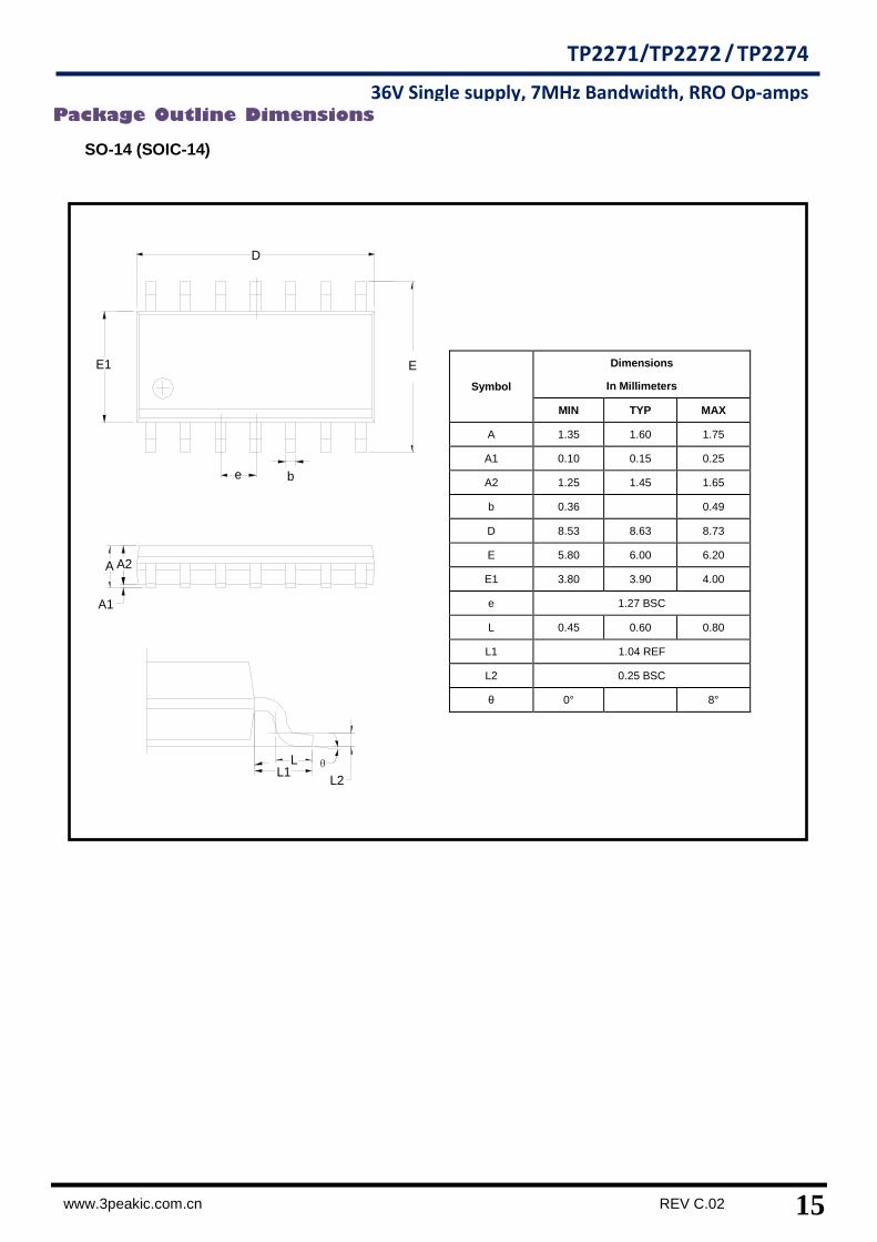
SO-14 (SOIC-14)
Symbol
Dimensions
In Millimeters
MIN TYP MAX
A 1.35 1.60 1.75
A1 0.10 0.15 0.25
A2 1.25 1.45 1.65
b 0.36 0.49
D 8.53 8.63 8.73
E 5.80 6.00 6.20
E1 3.80 3.90 4.00
e 1.27 BSC
L 0.45 0.60 0.80
L1 1.04 REF
L2 0.25 BSC
θ 0° 8°
16 REV C.02
www.3peakic.com.cn
TP2271 / TP2272 / TP2274
36V Single supply, 7MHz Bandwidth, RRO Op-amps
Package Outline Dimensions
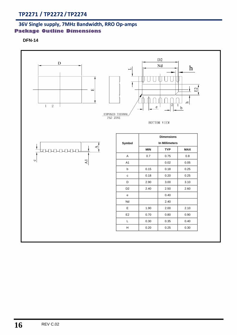
DFN-14
Symbol
Dimensions
In Millimeters
MIN TYP MAX
A 0.7 0.75 0.8
A1 0.02 0.05
b 0.15 0.18 0.25
c 0.18 0.20 0.25
D 2.90 3.00 3.10
D2 2.40 2.50 2.60
e 0.40
Nd 2.40
E 1.90 2.00 2.10
E2 0.70 0.80 0.90
L 0.30 0.35 0.40
H 0.20 0.25 0.30