Thermionic Emmision in Abrupt Junction Diffusion … 5: I-V of Heterojunction diodes 2011-01-19...
15
Lecture 5: I-V of Heterojunction diodes 2011-01-19 1 Lecture 5, High Speed Devices 2011 •Thermionic Emmision in Abrupt Junction •Diffusion current in graded Junctions •Generation Currents •Iso-type Junctions
Transcript of Thermionic Emmision in Abrupt Junction Diffusion … 5: I-V of Heterojunction diodes 2011-01-19...

Lecture 5: I-V of Heterojunction diodes
2011-01-19 1Lecture 5, High Speed Devices 2011
•Thermionic Emmision in Abrupt Junction•Diffusion current in graded Junctions•Generation Currents•Iso-type Junctions

Thermionic Emission, Metal-semiconductor junction
2011-01-19 2Lecture 5, High Speed Devices 2011
Ef
φs
φb Va
φs
φb Assumption: Carriers with an energy over s are able to pass over the barrier.
22
0
*
3
2**
2*
/1204
1expexp
KcmAm
m
h
kmA
kT
qV
kT
qTAJ
ee
bth
A* is Richardson’s constant
Forward Bias
Reverse Bias

Thermionic Emission, Metal-semiconductor junction
2011-01-19 3Lecture 5, High Speed Devices 2009
Ef
φsΦb’
VaN
φs
1expexp
'2*
kT
qV
kT
qTAJ anb
th
Identify Φb’ and VaN for p+N junction
Forward Bias
Reverse Bias
Φb’
1)1
exp()/exp(
1
1
'2*
1
1
'
K
V
kT
qkTqTAAI
N
NK
VN
N
N
NV
N
N
qN
N
q
EE
q
aBDd
ap
dN
a
ap
dN
ap
dNan
ap
dNN
ap
dNpcgpNNOB

Graded junctions I: Quasi Fermi Levels
2011-01-19 4Lecture 5, High Speed Devices 2011
ia
i
fpv
v
cfn
c
nkT
qVnnp
kT
EENp
kT
EENn
)exp(
)exp(
)exp(
Fermi levels are only defined under equilibrium conditions
For device under external bias, we define quasi-fermi-levels:
Efn
Efp
XN-Xp
Va
XN, Xp: depletion width edge
Efn: Fermi-level for electronsEfp: Fermi-level for holes

2 minute exercise: Quasi Fermi level
2011-01-19 5Lecture 5, High Speed Devices 2011
-Xp
Xn
EfnEfp
-Xp
Xn
-Xp Xn
log
(n,p
)
HolesElectrons
Equilibriumconcentrations
Add out of equilibriumn,p concentrations!
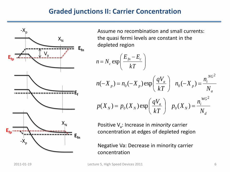
Graded junctions II: Carrier Concentration
2011-01-19 6Lecture 5, High Speed Devices 2011
Assume no recombination and small currents: the quasi fermi levels are constant in the depleted region
Efn
Efp
XN
-Xp
Va
-Xp
XN
Efn
Ef
Efp
d
WG
iN
aNN
a
NG
ip
app
N
nXp
kT
qVXpXp
N
nXn
kT
qVXnXn
2
00
2
00
)(exp)()(
)(exp)()(
Positive Va: Increase in minority carrier concentration at edges of depleted region
Negative Va: Decrease in minority carrierconcentration
kT
EENn
cfn
c exp
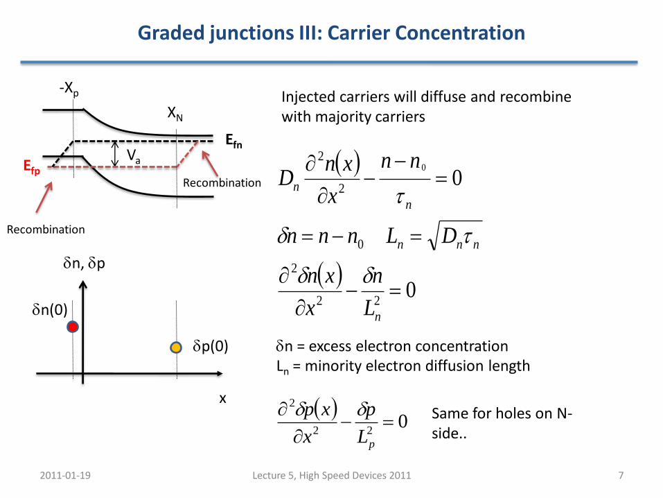
Graded junctions III: Carrier Concentration
2011-01-19 7Lecture 5, High Speed Devices 2011
Injected carriers will diffuse and recombine with majority carriers
Efn
Efp
XN
-Xp
Va
0
0
22
2
0
2
20
n
nnn
n
n
L
n
x
xn
DLnnn
nn
x
xnD
n = excess electron concentrationLn = minority electron diffusion length
0
22
2
pL
p
x
xp Same for holes on N-side..
x
n, p
n(0)
p(0)
Recombination
Recombination

Graded junctions IV: Carrier Concentration (Long diode)
2011-01-19 8Lecture 5, High Speed Devices 2011
Boundary value problem, 2nd order:
Efn
Efp
XN
-Xp
Va
x
n, p
n(0)
p(0)
1exp
0
0kT
qVpXp
p
aN
n
na
a
NG
i
p
Na
d
WG
i
L
XX
kT
qV
N
nxn
L
XX
kT
qV
N
nxp
exp1exp
exp1exp
2
2
NXx
pXx
p(0)
n(0)
For GaAs:~1nsDn~25 cm2/sDp~1 cm2/sLn=1.6 mmLp=0.3 mm

Graded junctions: Evaluation of current (Long diode)
2011-01-19 9Lecture 5, High Speed Devices 2011
Efn
Efp
XN
-Xp
Va
x
n, p
n(0)
p(0)
1exp
22
kT
qV
N
n
L
D
N
n
L
DqAI a
a
NG
i
n
n
d
WG
i
p
p
dD
x
XpqDpq
x
pqDJ N
pXxpppN
m
0minority
x
XnqDnq
x
nqDJ
p
nXxnnnp
m
Hole current Electron current
?
NXxnnn nqx
nqDJ m
Majority n>>0
0
We not not evaulate the electron current on the N-side, since:
Dn>Dp, niWG>>ni
NG

2 minute exercise: el/hole currents
2011-01-19 10Lecture 5, High Speed Devices 2011
-Xp
Xn
EfNEfp
x
XpqDJ N
pp
x
XnqDJ
p
nn
Assume that the diode has Dn=Dp and Ln=Lp
Which one is correct:
A Jp = Jn
B Jp >> Jn
C Jn >> Jp
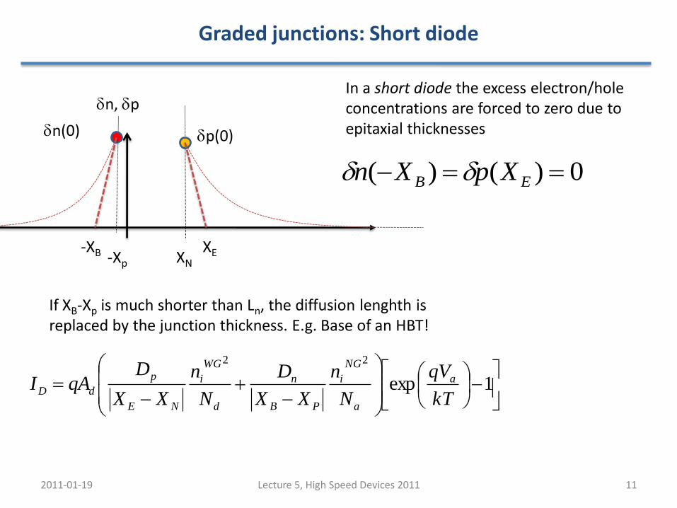
Graded junctions: Short diode
2011-01-19 11Lecture 5, High Speed Devices 2011
n, p
n(0) p(0)
If XB-Xp is much shorter than Ln, the diffusion lenghth is replaced by the junction thickness. E.g. Base of an HBT!
-Xp XN
XE-XB
0)()( EB XpXn
In a short diode the excess electron/hole concentrations are forced to zero due to epitaxial thicknesses
1exp
22
kT
qV
N
n
XX
D
N
n
XX
DqAI a
a
NG
i
PB
n
d
WG
i
NE
p
dD

Recombination in forward bias
2011-01-19 12Lecture 5, High Speed Devices 2011
p+ region: p >> n
)2( i
i
npn
nnpU
Recombination rate, SRH
N
p
X
WG
X
NG
rec xdxUqxdxUqJ0
0
)()(
kT
qVJ
kT
xEE
kT
qVn
nU a
rec
ifaNG
i
NG exp
expexp
N region: n=p gives Umax
kT
qVJ
kT
qVn
U arec
aWG
iWG
2exp
2
2exp
max
h=1
h=2
Depending on which term is dominating, 1<h<2, usually h~2For a p+N junction, the hole current is usually dominated by recombination

Generation in reverse bias
2011-01-19 13Lecture 5, High Speed Devices 2011
ii
i
npnn
npn
nnpU i
,
2)2(
2
Generation Rate, SRH
N
p
X
X
gen xdxUqJ )(
abipN
igen VXX
qnJ
2
V
I
kT
qVI a
Dh
exp

Summary for p+N diode
2011-01-19 14Lecture 5, High Speed Devices 2011
In a p+N junction, the current is essentially set by the electrons!Reverse current increases due to generation
1exp0
kT
qVII a
Dh
ap
dN
N
N
h 1
1 Graded Junction
Abrupt Junction
V
I
kT
qVI a
Dh
exp
agenD VIII 0
If recombination is important: 1<h<2
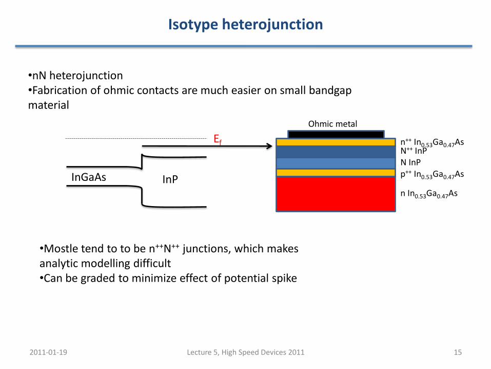
Isotype heterojunction
2011-01-19 15Lecture 5, High Speed Devices 2011
•nN heterojunction•Fabrication of ohmic contacts are much easier on small bandgap material
InPInGaAs
Ef
•Mostle tend to to be n++N++ junctions, which makes analytic modelling difficult•Can be graded to minimize effect of potential spike
N InPp++ In0.53Ga0.47As
n In0.53Ga0.47As
N++ InPn++ In0.53Ga0.47As
Ohmic metal