Theory and Practice of Electron Diffraction - Zuo Research...
36
DOE BES/DMS Materials Science and Engineering/Frederick Seitz Materials Research Laboratory J. M. Zuo Dept. of Materials and Engineering and Materials Research Laboratory University of Illinois at Urbana and Champaign 1304 W Green Street, Urbana, IL61801 [email protected] http://cbed.mse.uiuc.edu Theory and Practice of Electron Diffraction
Transcript of Theory and Practice of Electron Diffraction - Zuo Research...
DOE BES/DMS Materials Science and Engineering/Frederick Seitz Materials Research Laboratory
J. M. Zuo Dept. of Materials and Engineering and Materials
Research LaboratoryUniversity of Illinois at Urbana and Champaign
1304 W Green Street, Urbana, [email protected]
http://cbed.mse.uiuc.edu
Theory and Practice of Electron Diffraction
DOE BES/DMS Materials Science and Engineering/Frederick Seitz Materials Research Laboratory
Covered Topics
• Electron diffraction• Crystal diffraction patterns • Kikuchi Lines• Convergent beam electron diffraction• Electron nanobeam diffraction and examples
DOE BES/DMS Materials Science and Engineering/Frederick Seitz Materials Research Laboratory
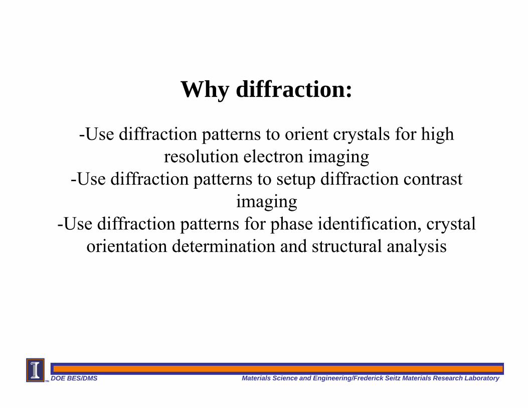
Why diffraction:
-Use diffraction patterns to orient crystals for high resolution electron imaging
-Use diffraction patterns to setup diffraction contrast imaging
-Use diffraction patterns for phase identification, crystal orientation determination and structural analysis
DOE BES/DMS Materials Science and Engineering/Frederick Seitz Materials Research Laboratory
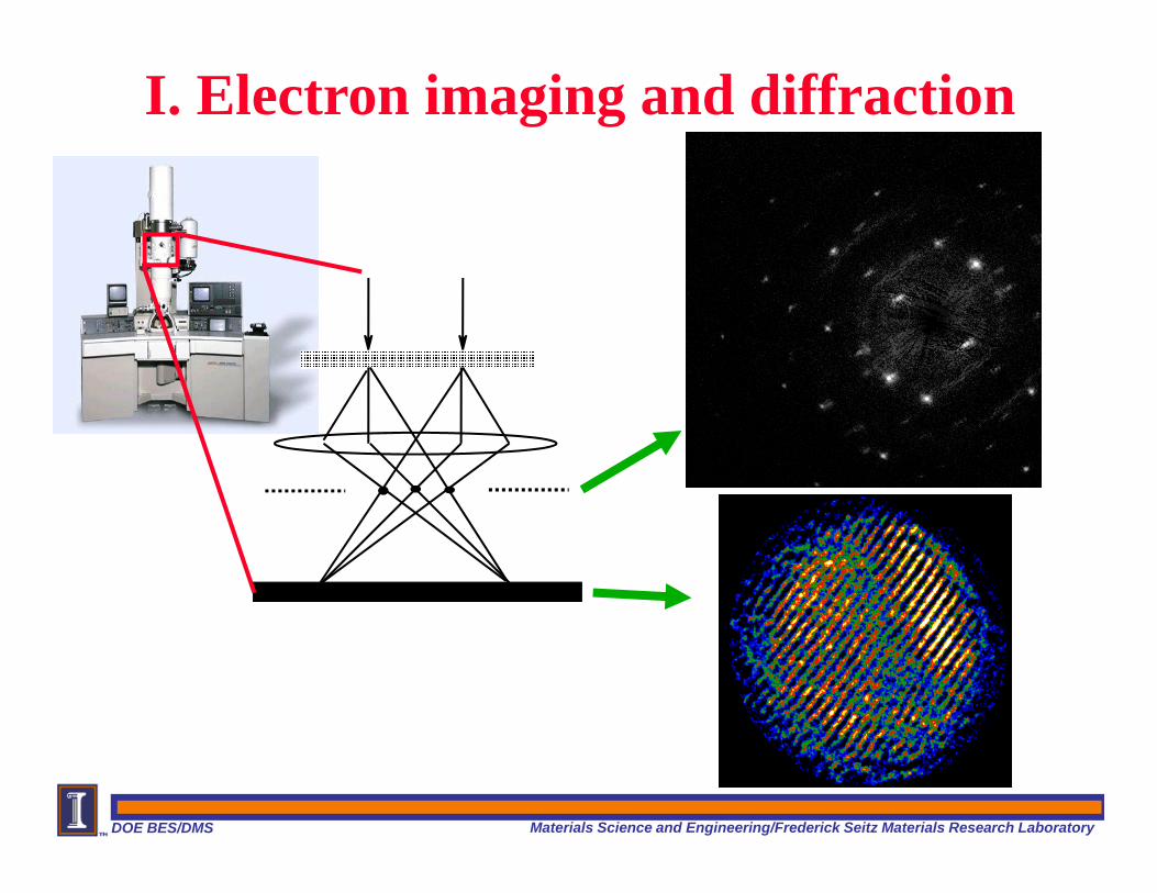
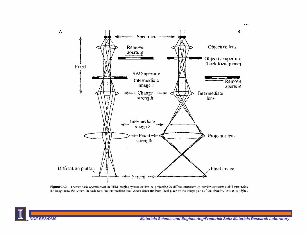
I. Electron imaging and diffraction
DOE BES/DMS Materials Science and Engineering/Frederick Seitz Materials Research Laboratory
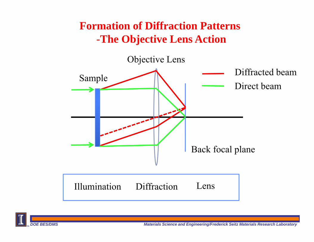
Direct beamDiffracted beam
Back focal plane
Objective Lens
Sample
Formation of Diffraction Patterns -The Objective Lens Action
Illumination Diffraction Lens
DOE BES/DMS Materials Science and Engineering/Frederick Seitz Materials Research Laboratory
DOE BES/DMS Materials Science and Engineering/Frederick Seitz Materials Research Laboratory
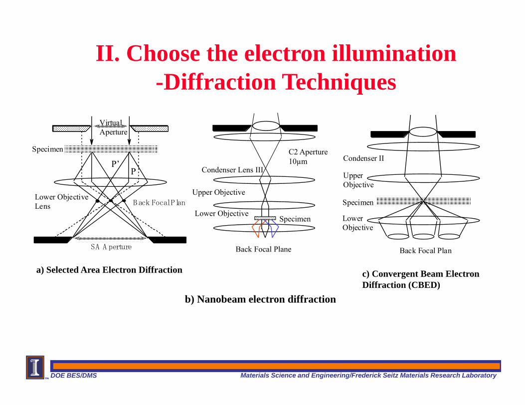
SA A perture
VirtualAperture
Specimen
Lower ObjectiveLens B ack FocalPlan
a) Selected Area Electron Diffraction
Specimen
nBack Focal Pla
ICondenser I
UpperObjective
LowerObjective
c) Convergent Beam Electron Diffraction (CBED)
Upper Objective
Lower ObjectiveSpecimen
Condenser Lens III
C2 Aperture10µm
Back Focal Plane
b) Nanobeam electron diffraction
PP’
II. Choose the electron illumination-Diffraction Techniques
DOE BES/DMS Materials Science and Engineering/Frederick Seitz Materials Research Laboratory
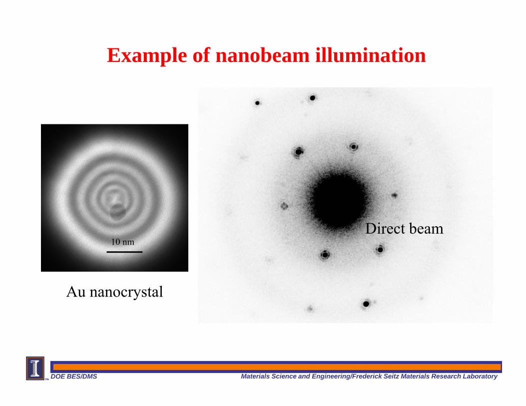
10 nm
Example of nanobeam illumination
Direct beam
Au nanocrystal

DOE BES/DMS Materials Science and Engineering/Frederick Seitz Materials Research Laboratory
CBED
DOE BES/DMS Materials Science and Engineering/Frederick Seitz Materials Research Laboratory
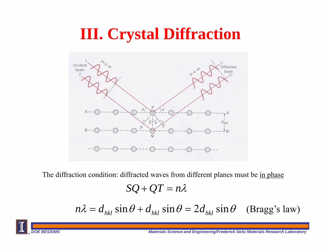
III. Crystal Diffraction
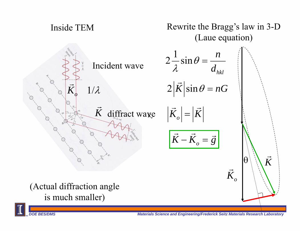
The diffraction condition: diffracted waves from different planes must be in phase
SQ QT nλ+ =
sin sin 2 sinhkl hkl hkln d d dλ θ θ θ= + = (Bragg’s law)
DOE BES/DMS Materials Science and Engineering/Frederick Seitz Materials Research Laboratory
Inside TEM
(Actual diffraction angle is much smaller)
Rewrite the Bragg’s law in 3-D (Laue equation)
12 sinhkl
nd
θλ
=
2 sinK nGθ =r
1/oK λr
Kr
oK K=r r
Incident wave
diffract wave
oK K g− =r r r
oKr
oKr
oKr K
rθ
DOE BES/DMS Materials Science and Engineering/Frederick Seitz Materials Research Laboratory
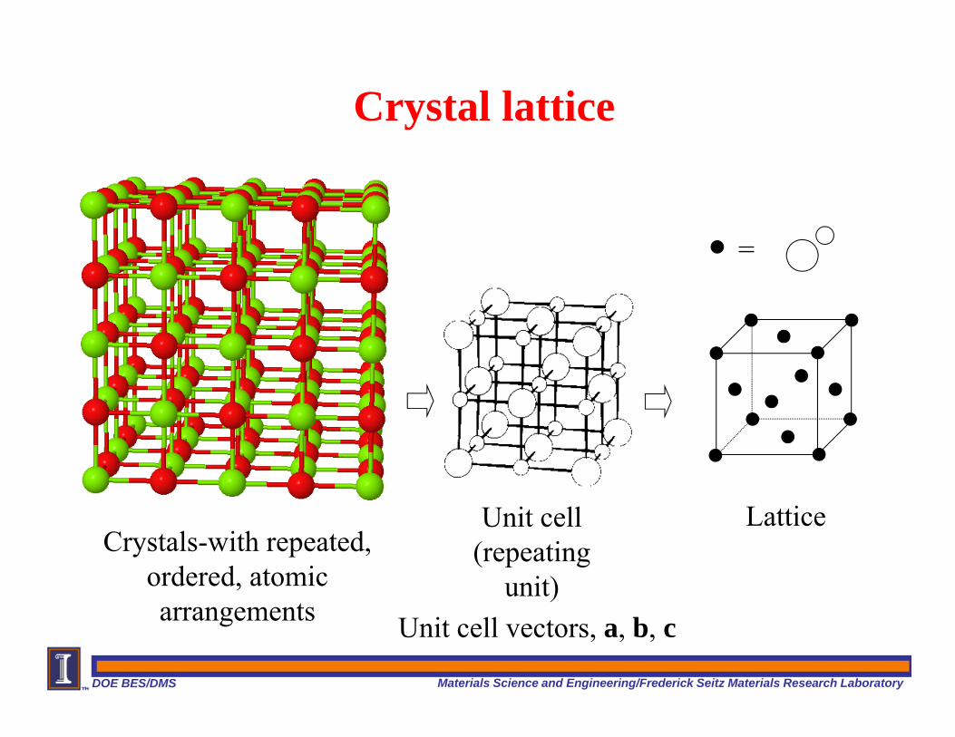
Crystal lattice
=
LatticeCrystals-with repeated,
ordered, atomic arrangements
Unit cell (repeating
unit)Unit cell vectors, a, b, c
DOE BES/DMS Materials Science and Engineering/Frederick Seitz Materials Research Laboratory
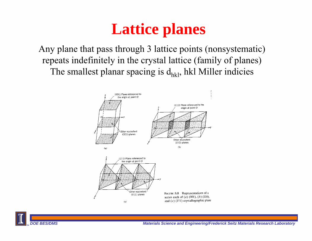
Lattice planesAny plane that pass through 3 lattice points (nonsystematic) repeats indefinitely in the crystal lattice (family of planes)
The smallest planar spacing is dhkl, hkl Miller indicies
DOE BES/DMS Materials Science and Engineering/Frederick Seitz Materials Research Laboratory
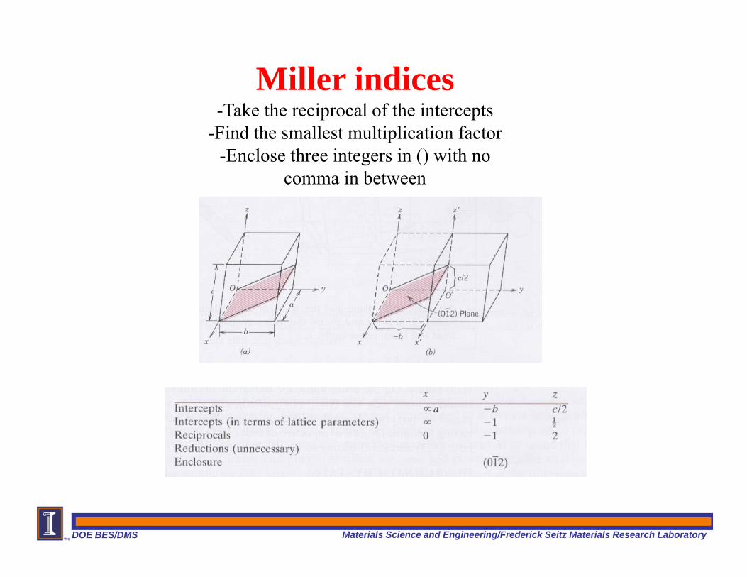
Miller indices-Take the reciprocal of the intercepts
-Find the smallest multiplication factor-Enclose three integers in () with no
comma in between
DOE BES/DMS Materials Science and Engineering/Frederick Seitz Materials Research Laboratory
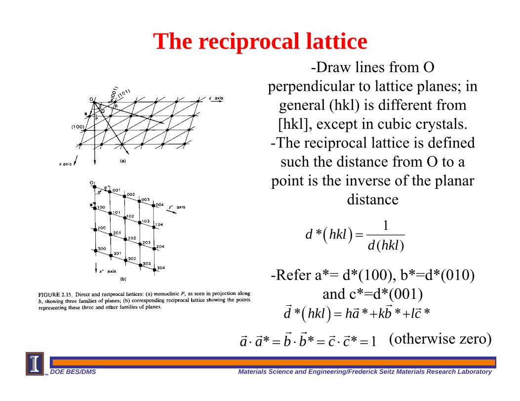
The reciprocal lattice-Draw lines from O
perpendicular to lattice planes; in general (hkl) is different from [hkl], except in cubic crystals.
-The reciprocal lattice is defined such the distance from O to a
point is the inverse of the planar distance
-Refer a*= d*(100), b*=d*(010) and c*=d*(001)
( ) 1*( )
d hkld hkl
=
( )* * * *d hkl ha kb lc= + +r rr r
* * * 1a a b b c c⋅ = ⋅ = ⋅ =r rr r r r (otherwise zero)
DOE BES/DMS Materials Science and Engineering/Frederick Seitz Materials Research Laboratory
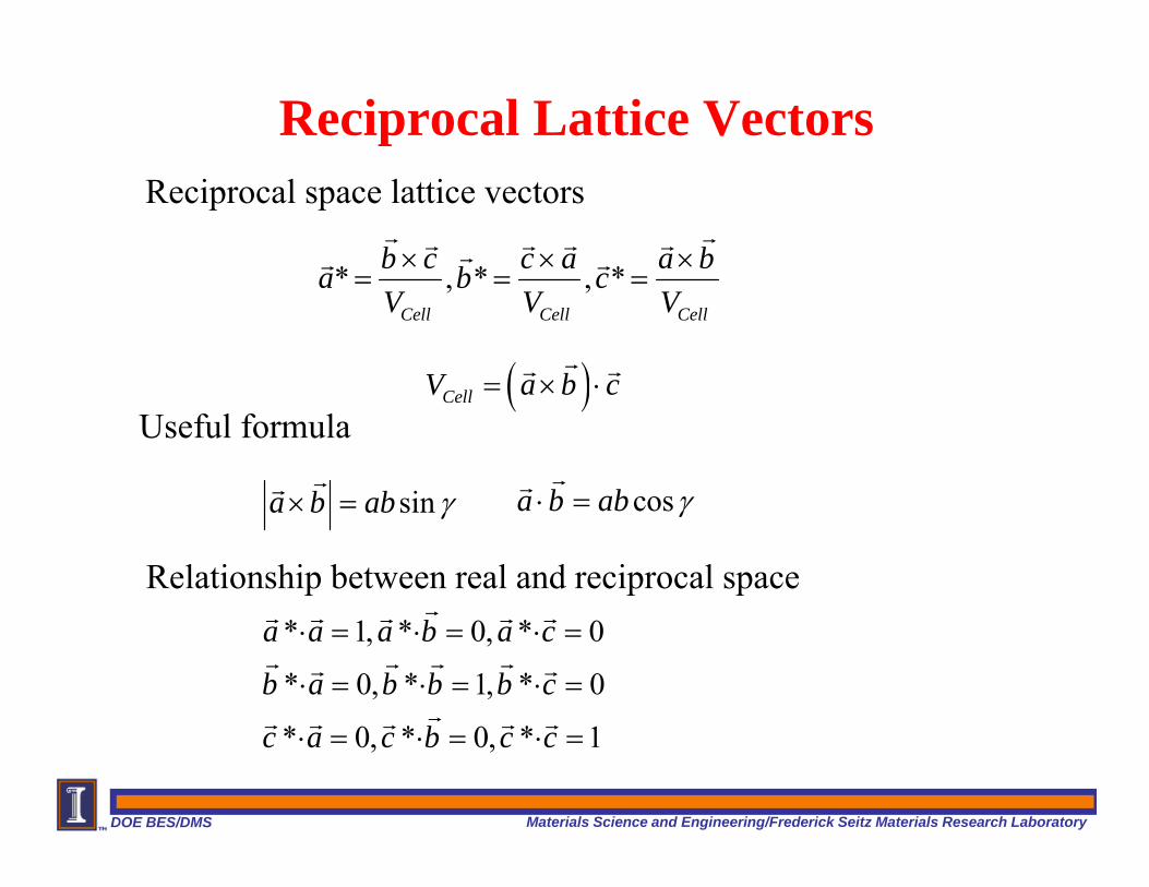
Reciprocal Lattice Vectors
* , * , *Cell Cell Cell
b c c a a ba b cV V V× × ×
= = =r rr r r rrr r
( )CellV a b c= × ⋅rr r
sina b ab γ× =rr
Useful formula
Reciprocal space lattice vectors
cosa b ab γ⋅ =rr
Relationship between real and reciprocal space* 1, * 0, * 0
* 0, * 1, * 0
* 0, * 0, * 1
a a a b a c
b a b b b c
c a c b c c
⋅ = ⋅ = ⋅ =
⋅ = ⋅ = ⋅ =
⋅ = ⋅ = ⋅ =
rr r r r r
r r r rr r
rr r r r r
DOE BES/DMS Materials Science and Engineering/Frederick Seitz Materials Research Laboratory
DOE BES/DMS Materials Science and Engineering/Frederick Seitz Materials Research Laboratory
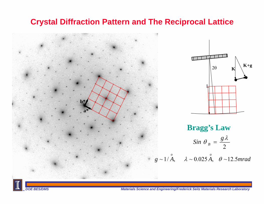
Crystal Diffraction Pattern and The Reciprocal Lattice
a*
b*
KK+g
L
2θ
2λθ gSin B =
Bragg’s Law
~ 1/ , ~ 0.025 , ~12.5o o
g A A mradλ θ
DOE BES/DMS Materials Science and Engineering/Frederick Seitz Materials Research Laboratory
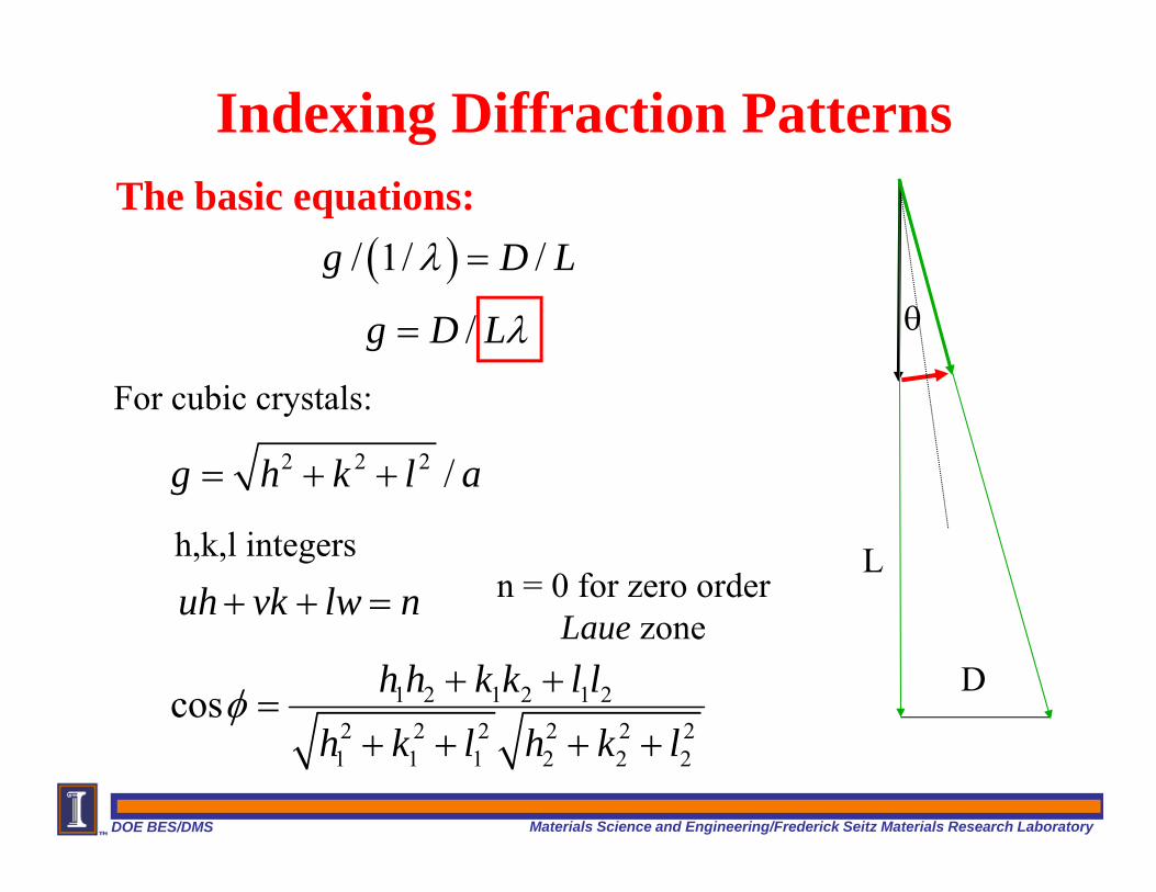
Indexing Diffraction PatternsThe basic equations:
θ
D
L
( )/ 1/ /g D Lλ =
/g D Lλ=
For cubic crystals:
2 2 2 /g h k l a= + +
h,k,l integers
uh vk lw n+ + = n = 0 for zero order Laue zone
1 2 1 2 1 22 2 2 2 2 2
1 1 1 2 2 2
cos h h k k l lh k l h k l
φ + +=
+ + + +
DOE BES/DMS Materials Science and Engineering/Frederick Seitz Materials Research Laboratory
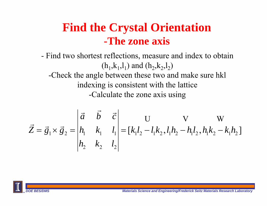
Find the Crystal Orientation-The zone axis
- Find two shortest reflections, measure and index to obtain (h1,k1,l1) and (h2,k2,l2)
-Check the angle between these two and make sure hkl indexing is consistent with the lattice
-Calculate the zone axis using
1 2 1 1 1 1 2 1 2 1 2 1 2 1 2 1 2
2 2 2
[ , , ]a b c
Z g g h k l k l l k l h h l h k k hh k l
= × = = − − −
rr r
r r rU V W
DOE BES/DMS Materials Science and Engineering/Frederick Seitz Materials Research Laboratory
DOE BES/DMS Materials Science and Engineering/Frederick Seitz Materials Research Laboratory
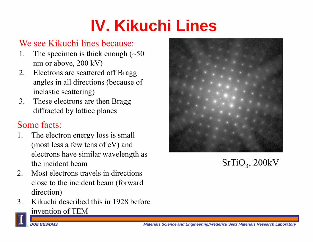
IV. Kikuchi LinesWe see Kikuchi lines because:1. The specimen is thick enough (~50
nm or above, 200 kV)2. Electrons are scattered off Bragg
angles in all directions (because of inelastic scattering)
3. These electrons are then Bragg diffracted by lattice planes
Some facts:1. The electron energy loss is small
(most less a few tens of eV) and electrons have similar wavelength as the incident beam
2. Most electrons travels in directions close to the incident beam (forward direction)
3. Kikuchi described this in 1928 before invention of TEM
SrTiO3, 200kV
DOE BES/DMS Materials Science and Engineering/Frederick Seitz Materials Research Laboratory
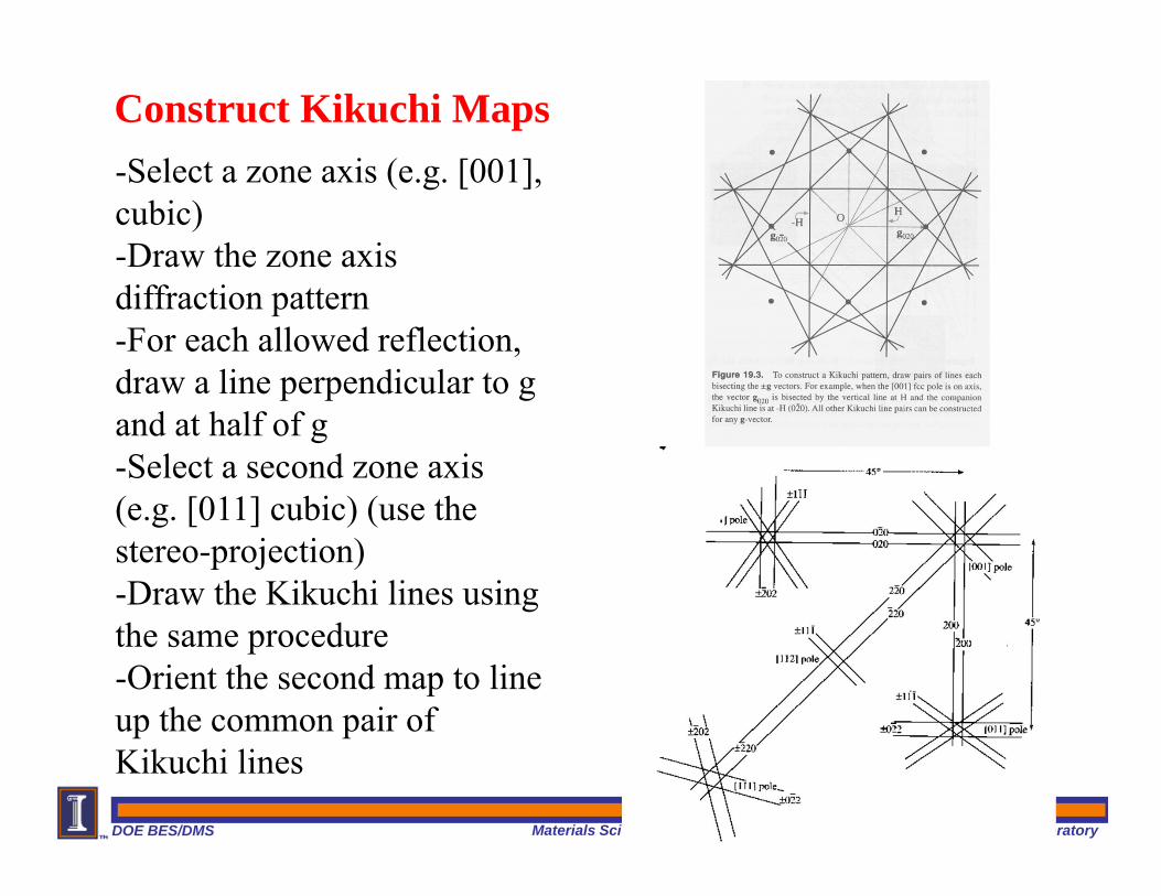
Construct Kikuchi Maps-Select a zone axis (e.g. [001], cubic)-Draw the zone axis diffraction pattern-For each allowed reflection, draw a line perpendicular to g and at half of g-Select a second zone axis (e.g. [011] cubic) (use the stereo-projection)-Draw the Kikuchi lines using the same procedure-Orient the second map to line up the common pair of Kikuchi lines
DOE BES/DMS Materials Science and Engineering/Frederick Seitz Materials Research Laboratory
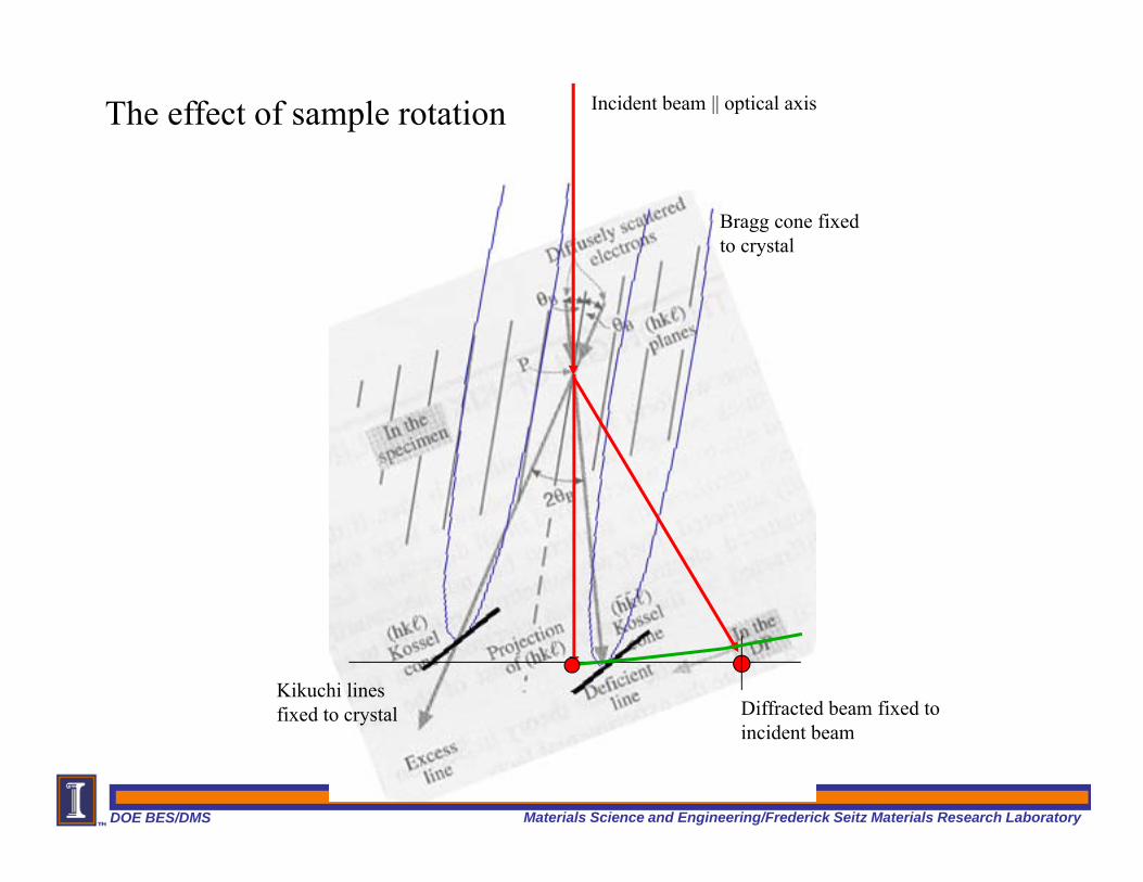
The effect of sample rotation Incident beam || optical axis
Diffracted beam fixed to incident beam
Bragg cone fixed to crystal
Kikuchi lines fixed to crystal
DOE BES/DMS Materials Science and Engineering/Frederick Seitz Materials Research Laboratory
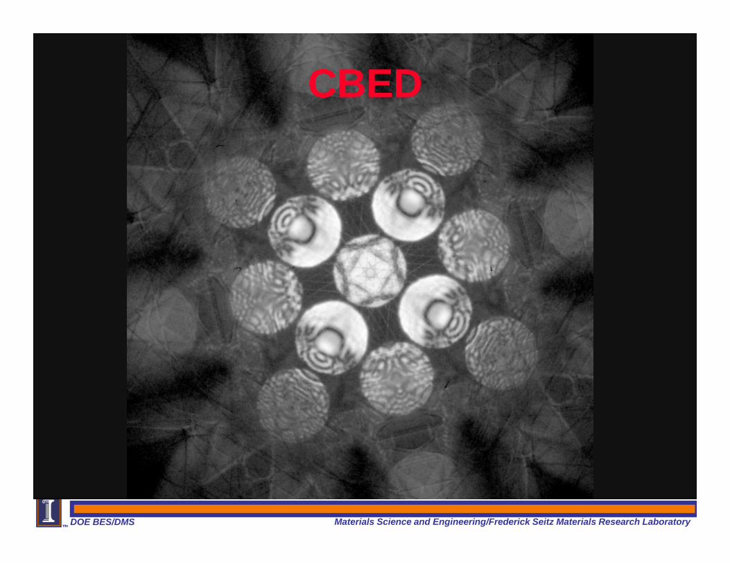
CBED
DOE BES/DMS Materials Science and Engineering/Frederick Seitz Materials Research Laboratory
Specimen
Back Focal Plan
Condenser II
Upper Objective
Lower Objective
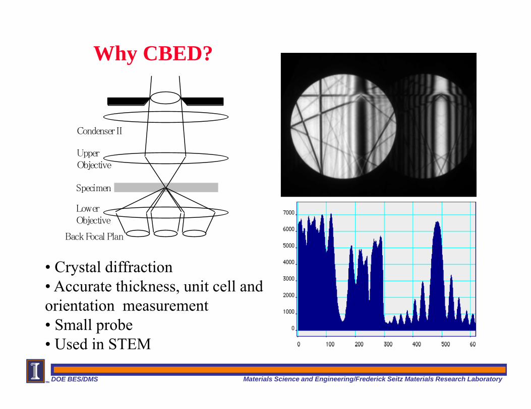
• Crystal diffraction• Accurate thickness, unit cell and orientation measurement• Small probe • Used in STEM
Why CBED?
DOE BES/DMS Materials Science and Engineering/Frederick Seitz Materials Research Laboratory
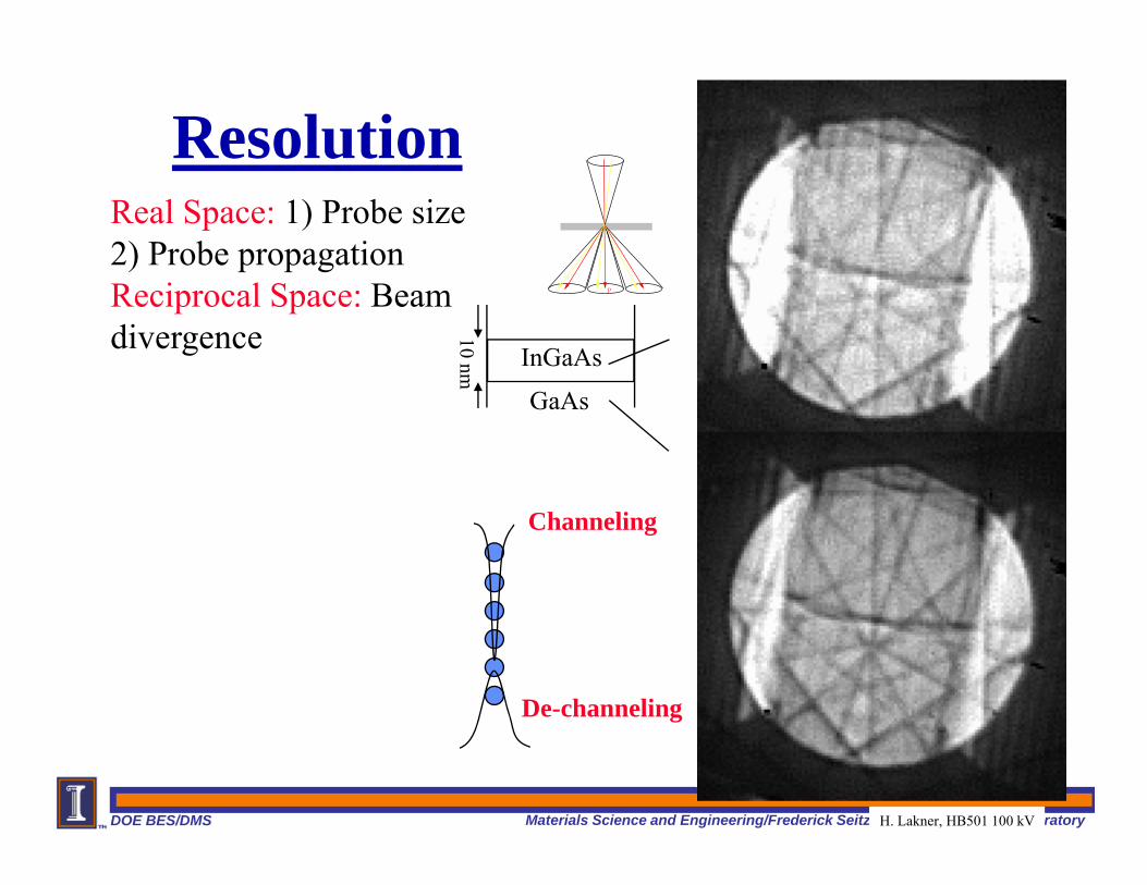
GaAs
InGaAs
10 nm
H. Lakner, HB501 100 kV
Real Space: 1) Probe size 2) Probe propagationReciprocal Space: Beam divergence
Resolution
Channeling
De-channeling
PP'
DOE BES/DMS Materials Science and Engineering/Frederick Seitz Materials Research Laboratory
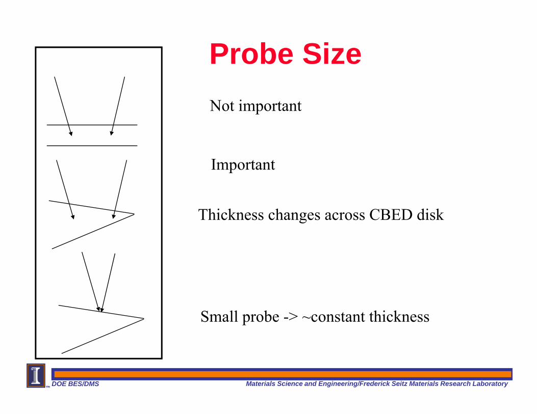
Probe SizeNot important
Important
Thickness changes across CBED disk
Small probe -> ~constant thickness
DOE BES/DMS Materials Science and Engineering/Frederick Seitz Materials Research Laboratory
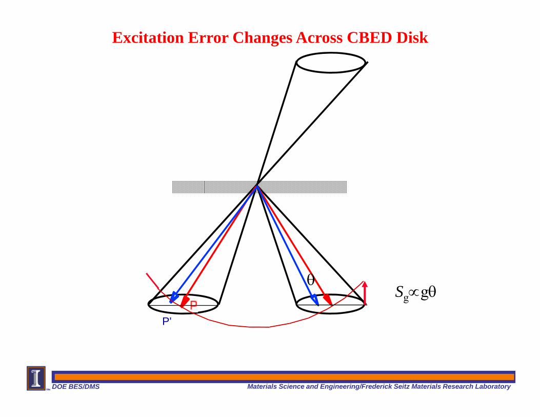
P'
Sg∝gθθ
Excitation Error Changes Across CBED Disk
DOE BES/DMS Materials Science and Engineering/Frederick Seitz Materials Research Laboratory
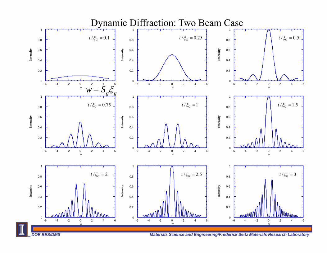
0
0.2
0.4
0.6
0.8
1
-6 -4 -2 0 2 4 6W
Inte
nsity
0
0.2
0.4
0.6
0.8
1
-6 -4 -2 0 2 4 6W
Inte
nsity
0
0.2
0.4
0.6
0.8
1
-6 -4 -2 0 2 4 6W
Inte
nsity
0
0.2
0.4
0.6
0.8
1
-6 -4 -2 0 2 4 6W
Inte
nsity
0
0.2
0.4
0.6
0.8
1
-6 -4 -2 0 2 4 6W
Inte
nsity
0
0.2
0.4
0.6
0.8
1
-6 -4 -2 0 2 4 6W
Inte
nsity
0
0.2
0.4
0.6
0.8
1
-6 -4 -2 0 2 4 6W
Inte
nsity
0
0.2
0.4
0.6
0.8
1
-6 -4 -2 0 2 4 6W
Inte
nsity
0
0.2
0.4
0.6
0.8
1
-6 -4 -2 0 2 4 6W
Inte
nsity
t /ξG = 0.1 t /ξG = 0.25 t /ξG = 0.5
t /ξG = 0.75 t /ξG =1 t /ξG =1.5
t /ξG = 2 t /ξG = 2.5 t /ξG = 3
Dynamic Diffraction: Two Beam Case
g gw S ξ=
DOE BES/DMS Materials Science and Engineering/Frederick Seitz Materials Research Laboratory
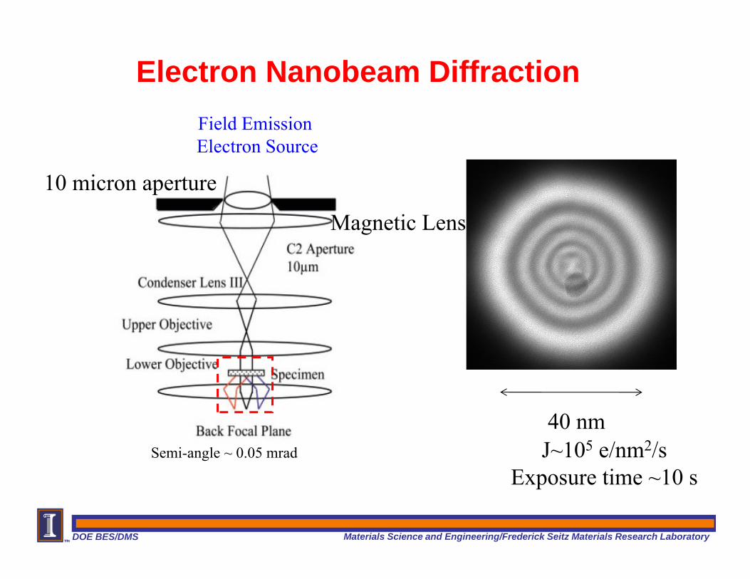
Electron Nanobeam DiffractionField Emission Electron Source
Semi-angle ~ 0.05 mrad
Magnetic Lens
10 micron aperture
40 nmJ~105 e/nm2/s
Exposure time ~10 s
DOE BES/DMS Materials Science and Engineering/Frederick Seitz Materials Research Laboratory
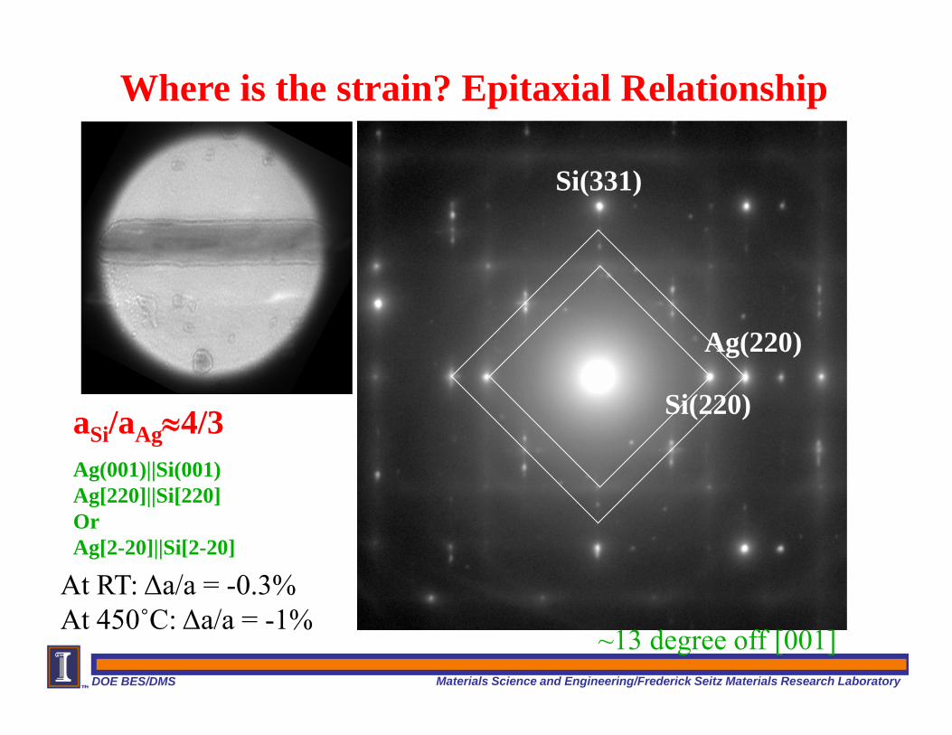
Si(220)
Ag(220)
Where is the strain? Epitaxial Relationship
aSi/aAg≈4/3Ag(001)||Si(001)Ag[220]||Si[220]OrAg[2-20]||Si[2-20]
Si(331)
~13 degree off [001]
At RT: Δa/a = -0.3%At 450˚C: Δa/a = -1%
DOE BES/DMS Materials Science and Engineering/Frederick Seitz Materials Research Laboratory
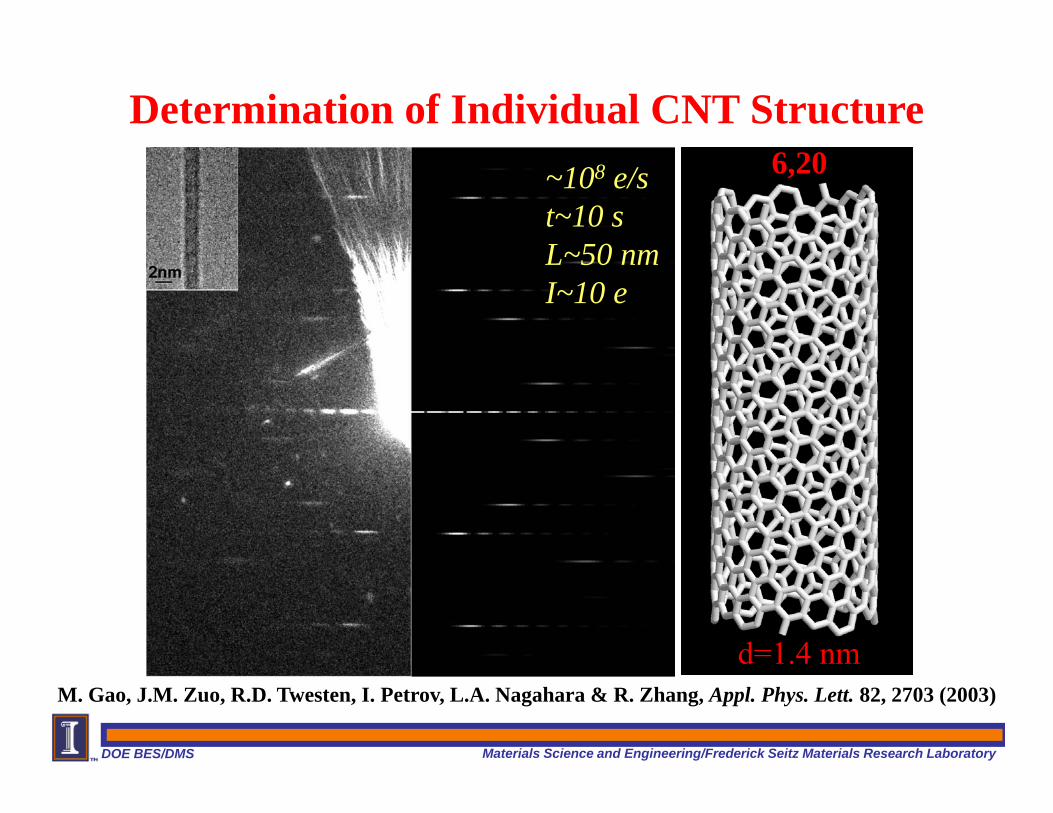
Determination of Individual CNT Structure
M. Gao, J.M. Zuo, R.D. Twesten, I. Petrov, L.A. Nagahara & R. Zhang, Appl. Phys. Lett. 82, 2703 (2003)
6,20~108 e/st~10 sL~50 nmI~10 e
d=1.4 nm
DOE BES/DMS Materials Science and Engineering/Frederick Seitz Materials Research Laboratory
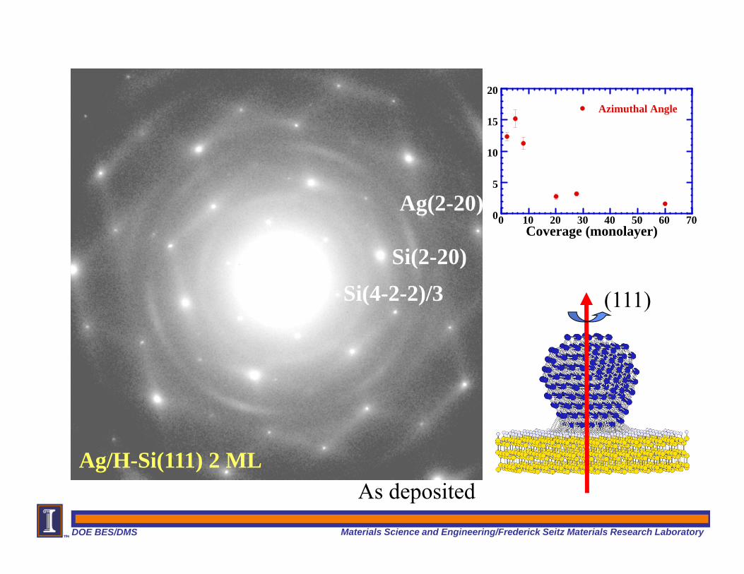
Ag/H-Si(111) 2 ML
Si(2-20)Si(4-2-2)/3
Ag(2-20)
(111)
0
5
10
15
20
0 10 20 30 40 50 60 70
Azimuthal Angle
Coverage (monolayer)
As deposited
DOE BES/DMS Materials Science and Engineering/Frederick Seitz Materials Research Laboratory
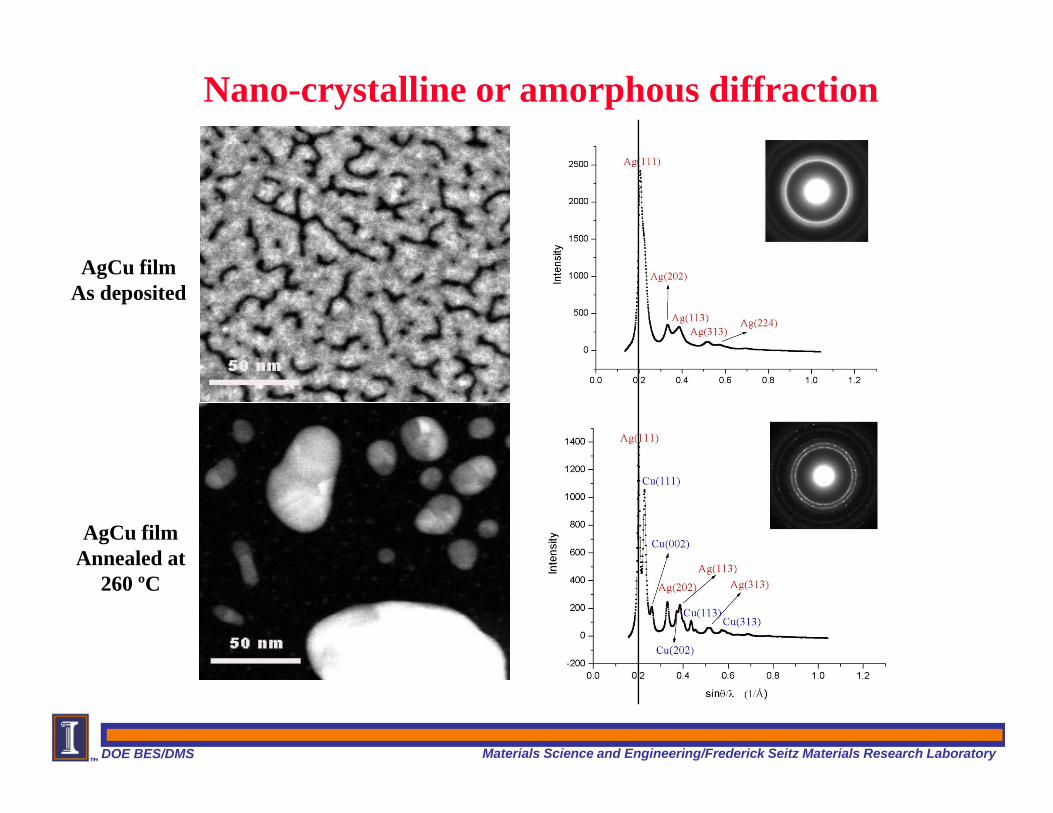
Nano-crystalline or amorphous diffraction
AgCu filmAs deposited
AgCu filmAnnealed at
260 ºC
DOE BES/DMS Materials Science and Engineering/Frederick Seitz Materials Research Laboratory
References
D.B. Williams and C. B. Carter, Transmission Electron Microscopy, Plenum, New York (1996)
J.W. Edington, Practical Electron Microscopy in Materials Science, Monograph 2, Electron Diffraction in the Electron Microscope, Philips Technical Library (1975)
J.M. Cowley, Diffraction Physics, North-Holland, New York (1981)
J.C.H. Spence and J.M. Zuo, Electron Microdiffraction, Plenum, New York (1992)