The Future of Electronics: Post-Silicon Logic and Memory
33
IBM T. J. Watson Research Center © 2006 IBM Corporation The Future of Electronics: The Future of Electronics: Post Post- Silicon Logic and Memory Silicon Logic and Memory Thomas N. Theis, Director, Physical Sciences, IBM Research
Transcript of The Future of Electronics: Post-Silicon Logic and Memory

IBM T. J. Watson Research Center
© 2006 IBM Corporation
The Future of Electronics:The Future of Electronics:PostPost--Silicon Logic and MemorySilicon Logic and Memory
Thomas N. Theis, Director, Physical Sciences, IBM Research

IBM Research
© 2006 IBM Corporation2T.N. Theis to SSSC, October 19, 2006
Can we extend the IT revolution?
Organic Electronics?Moletronics? Spintronics?Plasmonics?
Quantum Computing?…?
principle features specified to: i1mm
i10 λmi100 nm
Information technology has progressed through continuous miniaturization and repeated invention of new devices to store, process, and communicate information.The transistor and other devices are now approaching hard physical limits.
What’s Next?

IBM Research
© 2006 IBM Corporation3T.N. Theis to SSSC, October 19, 2006
$1000 buys...
1.E-06
1.E-03
1.E+00
1.E+03
1.E+06
1.E+09
1.E+12
1880 1900 1920 1940 1960 1980 2000 2020
Year
Co
mp
uta
tion
s/se
c
MechanicalElectro-mechanicalVacuum tubeDiscrete transistorIntegrated circuit
Result: Ever-Decreasing Costs of Computation, Ever-Expanding Applications of Information Technology
After R. Kurzweil, 1999

IBM Research
© 2006 IBM Corporation4T.N. Theis to SSSC, October 19, 2006
Needed: New Devices Based on New Materials and New Physics.
Carbon nanotubes
Semiconductor nanowires
Chalcogenides
New (smaller, cheaper, faster) devices
Polymers
Complex Oxides

IBM Research
© 2006 IBM Corporation5T.N. Theis to SSSC, October 19, 2006
§ The extension of silicon CMOS technology
§ The search for the “ultimate” FET
§ “Beyond the FET”: the Nanoelectronics Research Initiative
§ A Personal Outlook:prospects for adiabatic switching and reversible logic
Topics

IBM Research
© 2006 IBM Corporation6T.N. Theis to SSSC, October 19, 2006
The silicon transistor in manufacturing …
35 nmGate Length
90 nm technology generation
IBM Research
© 2006 IBM Corporation7T.N. Theis to SSSC, October 19, 2006
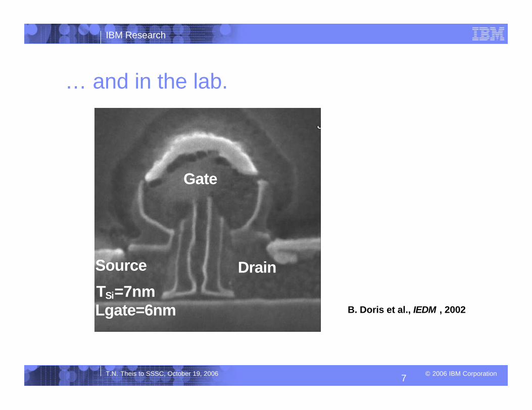
… and in the lab.
TSi=7nm Lgate=6nm
Source Drain
Gate
B. Doris et al., IEDM , 2002
IBM Research
© 2006 IBM Corporation8T.N. Theis to SSSC, October 19, 2006
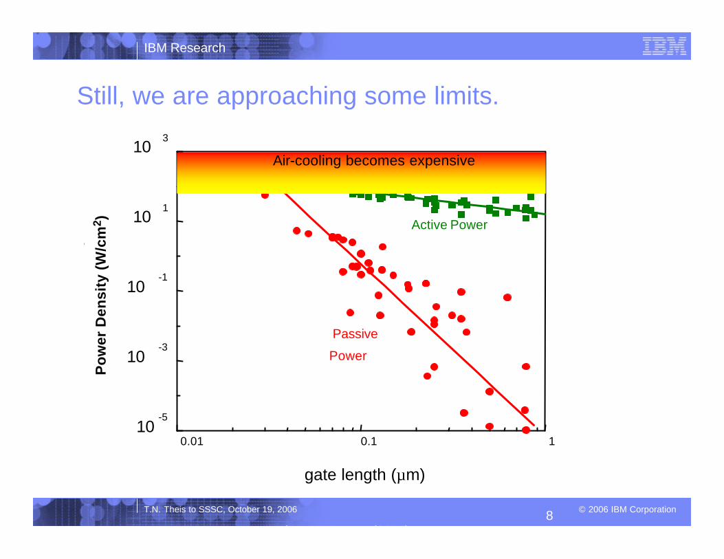
Still, we are approaching some limits.
E. Nowak, IBM J. R&D, (2002).
0.01 0.1 110
-5
10-3
10-1
101
103
pow
er (
W/c
m2 )
Active Power
Passive
Power
gate length (µm)
Po
wer
Den
sity
(W
/cm
2 )
Air-cooling becomes expensive
IBM Research
© 2006 IBM Corporation9T.N. Theis to SSSC, October 19, 2006
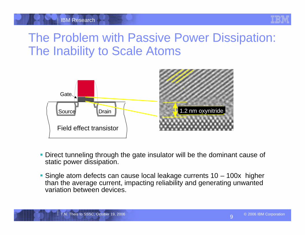
The Problem with Passive Power Dissipation:The Inability to Scale Atoms
§ Direct tunneling through the gate insulator will be the dominant cause of static power dissipation.
§ Single atom defects can cause local leakage currents 10 – 100x higher than the average current, impacting reliability and generating unwanted variation between devices.
Field effect transistor
Source Drain
Gate
1.2 nm oxynitride

IBM Research
© 2006 IBM Corporation10T.N. Theis to SSSC, October 19, 2006
Voltage-scaling regime
Insulator thickness and gate voltage no longer scaling
1.E-01
1.E+00
1.E+01
1.E+02
0.010.1110
Gate Length (um)
Sw
itch
ing
En
erg
y (f
J)
Switching energy is declining at a slower rate.
IBM Research
© 2006 IBM Corporation11T.N. Theis to SSSC, October 19, 2006
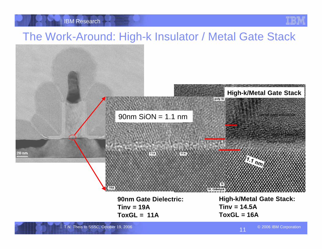
10S Tox=11A
High-k/Metal Gate Stack
90nm Gate Dielectric:Tinv = 19AToxGL = 11A
High-k/Metal Gate Stack:Tinv = 14.5AToxGL = 16A
90nm SiON = 1.1 nm
The Work-Around: High-k Insulator / Metal Gate Stack
Oxide interlayer
High-k material
Metal gate electrode

IBM Research
© 2006 IBM Corporation12T.N. Theis to SSSC, October 19, 2006
Innovation Will Continue:Transistor Roadmap Options
2004 2007 2010 2013 2016 2020
37 nm 25 nm 18 nm 13 nm 9 nm 6 nm Physical Gate
back-gate
channel
isolation
buried oxide
channel
top-gate
Double-Gate CMOS
Source Drain
Gate
depletion layer
isolation
buried oxidehalo
raised source/drain
Silicon Substrate
doped channel
High k gate dielectric FinFET
Strained Si, Ge, SiGe
isolation
buried oxide
Silicon Substrate
Ultrathin SOI
In general, growing power dissipation and increasing process variability will be addressed by introduction of new materials and device structures, and by design innovations in circuits
and system architecture.

IBM Research
© 2006 IBM Corporation13T.N. Theis to SSSC, October 19, 2006
SLm-1
SLm+1
SLm
WLn-1
WLn+1
WLn
Memory may be easier to shrink than logic.
§ Everyone is looking for a dense (cheap) cross-point memory.§ It is relatively easy to identify materials that show bistable hysteretic
behavior (easily distinguishable, stable on/off states).

IBM Research
© 2006 IBM Corporation14T.N. Theis to SSSC, October 19, 2006
Some Classes of Novel Memory Devices Under Development by Commercial Entities
§ Extensions of Silicon Nonvolatile (Flash) Memory § Magnetic Tunnel Junctions (MRAM)§ Chalcogenide Phase Change Materials (PCM) § Ferroelectric Polymers § Hysteretic Conduction in Complex Metal Oxides§ Solid-State Electrochemical Systems§ (Nano) Electro-Mechanical Systems§ and more …

IBM Research
© 2006 IBM Corporation15T.N. Theis to SSSC, October 19, 2006
Example: 16Mbit IBM MRAM Demonstration
• 4 active bits / block
• Good power supplydistribution
• Write currentstrimmed by block
Pads / peripheral circuits
Redundancy control &Write current trimming
Pads / peripheral circuits
8Mbunit
4 active 128Kb blocks
8Mbunit
• 4 active bits / block
• Good power supplydistribution
• Write currentstrimmed by block
Pads / peripheral circuits
Redundancy control &Write current trimming
Pads / peripheral circuits
8Mbunit
4 active 128Kb blocks
8Mbunit
Chip image: Cross-section:
MTJ
-150 -100 -50 0 50 100 150
1.00
1.20
1.40
1.60
1.80
2.00
2.20
2.40
Res
ista
nce
(a.u
.)
Field (Oe)
MR
(%)
-2000
20
40
60
80
100
120
140
1995
TMR
(%)
Field (Oe)
Materials Advances
-150 -100 -50 0 50 100 1500
50
100
150
200
250
300
350
400
TMR
(%)
290K
Field (Oe)Field (Oe)
2005
TMR
(%)
The Emerging Post-CMOS Landscape
© 2006 IBM Corporation16 T.N. Theis to SSSC, October 19, 2006
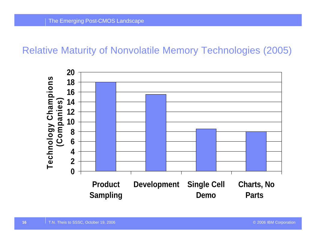
Relative Maturity of Nonvolatile Memory Technologies (2005)
02468
101214161820
ProductSampling
Development Single CellDemo
Charts, NoParts
Tech
nolo
gy C
ham
pion
s (C
ompa
nies
)
IBM Research
© 2006 IBM Corporation17T.N. Theis to SSSC, October 19, 2006
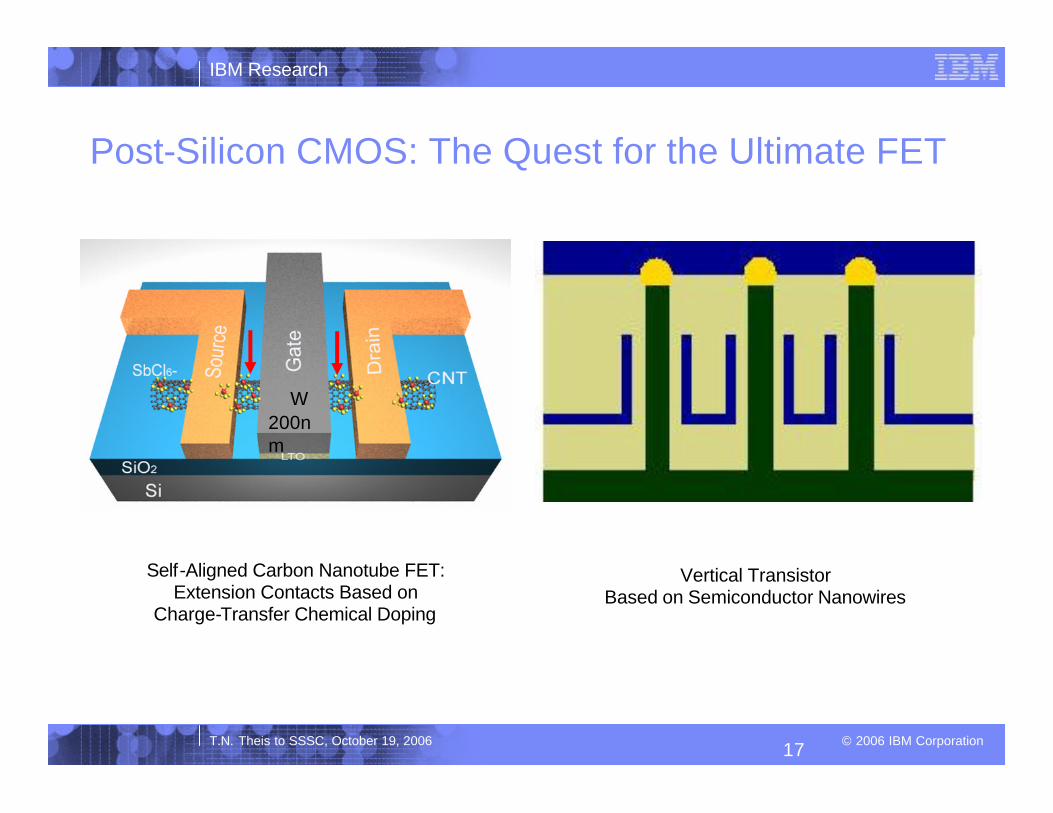
Post-Silicon CMOS: The Quest for the Ultimate FET
W200nm
Self-Aligned Carbon Nanotube FET: Extension Contacts Based on
Charge-Transfer Chemical Doping
Vertical Transistor Based on Semiconductor Nanowires

IBM Research
© 2006 IBM Corporation18T.N. Theis to SSSC, October 19, 2006
Vertical Silicon Nanowire FET
1 µm
Al gate
NW + dielectric
Vg Vsd

IBM Research
© 2006 IBM Corporation19T.N. Theis to SSSC, October 19, 2006
10-5
10-4
10-3
10-2
10-1
100
101
|I d| [
µA
]
-2 -1 0 1 2Vgs [V]
Vds -0.7 V -0.5 V -0.3 V -0.1 V
20
15
10
5
0
|I d| [
µA]
-1.2 -0.8 -0.4 0.0Vds [V]
-1.2 V
-0.8 V
-0.4 V
0 V 0.4 V
Vds = -1.6 V
12
8
4
0
gm
[µS
]
-2.0 -1.0 0.0 1.0Vgs [V]
90 K 300 K
Pd Pd
nanotube
Subthreshold Characteristics
Output Characteristics
Temperature dependence
Simple back-gated CNTFET
Intrinsic Performance of Cabon Nanotube FETs
Yu-Ming Lin et al. (IBM), EDL 2005

IBM Research
© 2006 IBM Corporation20T.N. Theis to SSSC, October 19, 2006
2m
Tg
gf
Cπ=Cut-off Frequency
260 GHz550 GHz800 GHzfT @ Lg = 65 nm
32 pF/m120 pF/m38 pF/mCg/L
3.5 µS27 µS12.5 µSMaximum gm
12-nm SiO28-nm HfO210-nm SiO2Gate Dielectric
~ 1.1 nm~ 1.7 nm~ 1.8 nmDiameter
Seidel et al. (Infineon)
Javey et al. (Stanford)
Lin et al.(IBM)
Cg : gate capacitance
Intrinsic Switching Speed of CNFETs
Yu-Ming Lin et al. (IBM), EDL 2005

IBM Research
© 2006 IBM Corporation21T.N. Theis to SSSC, October 19, 2006
Carbon Nanotube FET:Potential for greatly improved turn-on characteristics (low-voltage operation)
J. Appenzeller, Y.-M. Lin, J. Knoch, and Ph. Avouris, Phys. Rev. Lett. 93, 196805 (2004)
Dual-Gate CNTFET

IBM Research
© 2006 IBM Corporation22T.N. Theis to SSSC, October 19, 2006
Will there be a successor to the FET?
§ Many have written about this subject.
§ An article by George Bourianoff (“The Future of Nanocomputing”,IEEE Computer 36, pp. 44–53) sparked discussions within the Semiconductor Research Corporation regarding the objectives of a new research program – the Nanoelectronics Research Initiative (NRI) – which would stimulate the exploration of devices “beyond the FET”.
à computational state vectors other than electronic charge
IBM Research
© 2006 IBM Corporation23T.N. Theis to SSSC, October 19, 2006
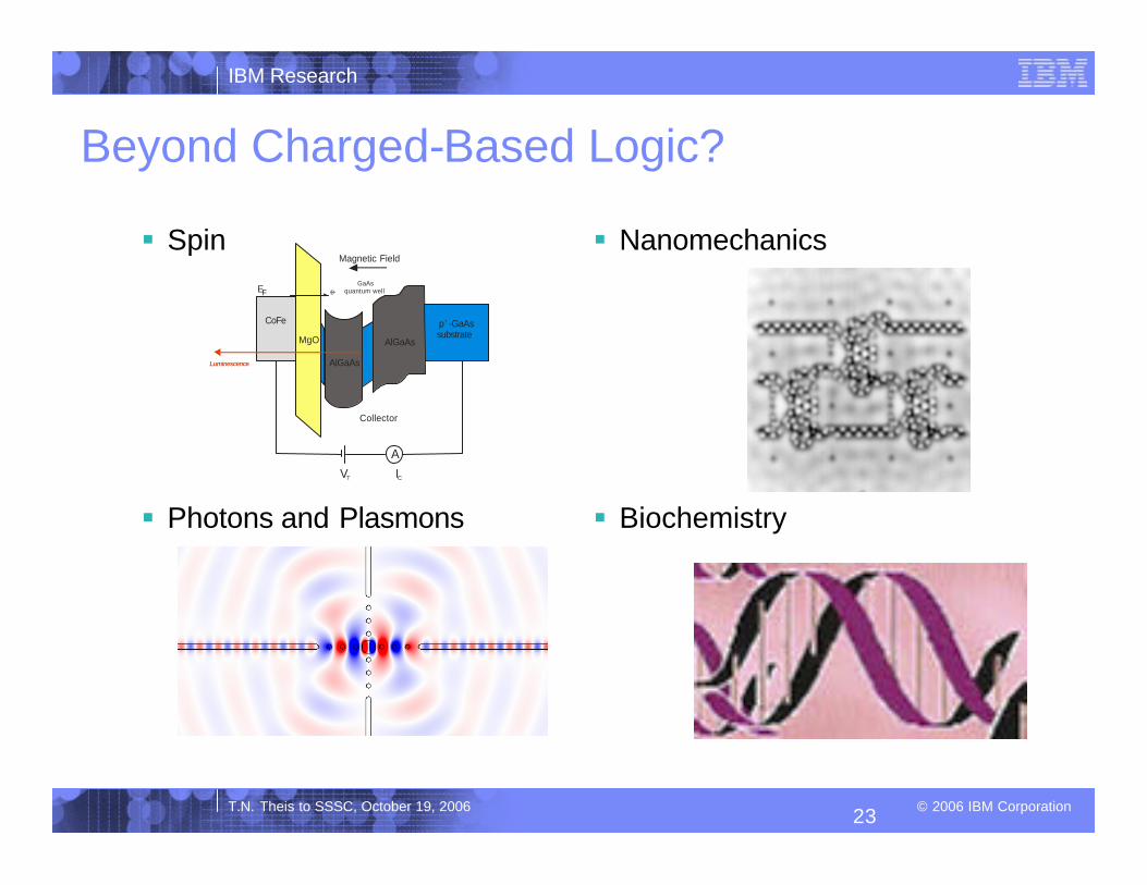
Beyond Charged-Based Logic?
§ Spin
§ Photons and Plasmons
§ Nanomechanics
§ Biochemistry
p -GaAssubstrate
+
AlGaAs
GaAsquantum wellEF
MgO
A
VT IC
CoFe
Collector
Magnetic Field
e-
Luminescence AlGaAs

IBM Research
© 2006 IBM Corporation24T.N. Theis to SSSC, October 19, 2006
Nanoelectronics Research Initiative (NRI)§ AMD, Freescale, Micron, TI, IBM, Intelà Joint Industry funding of University Research
§ Promoting both – Invention / Discovery (distributed research, “let many flowers bloom”)
– Proof of Concept (focused university consortia with outstanding facilities)
§ “Extend the historical cost/function reduction, along with increased performance and density … orders of magnitude beyond the limits of CMOS”– Computational State Vectors other than Electronic Charge
– Non-equilibrium Systems
– Novel Energy Transfer Mechanisms
– Nanoscale Thermal Management
– Directed Self-assembly of such structures
IBM Research
© 2006 IBM Corporation25T.N. Theis to SSSC, October 19, 2006
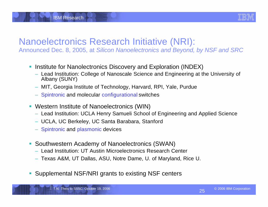
Nanoelectronics Research Initiative (NRI):Announced Dec. 8, 2005, at Silicon Nanoelectronics and Beyond, by NSF and SRC
§ Institute for Nanolectronics Discovery and Exploration (INDEX)– Lead Institution: College of Nanoscale Science and Engineering at the University of
Albany (SUNY) – MIT, Georgia Institute of Technology, Harvard, RPI, Yale, Purdue– Spintronic and molecular configurational switches
§ Western Institute of Nanoelectronics (WIN)– Lead Institution: UCLA Henry Samueli School of Engineering and Applied Science– UCLA, UC Berkeley, UC Santa Barabara, Stanford– Spintronic and plasmonic devices
§ Southwestern Academy of Nanoelectronics (SWAN)– Lead Institution: UT Austin Microelectronics Research Center– Texas A&M, UT Dallas, ASU, Notre Dame, U. of Maryland, Rice U.
§ Supplemental NSF/NRI grants to existing NSF centers

26
NSF/NRI Supplemental Awards: 2005
Nanoferroelectric Random Access Memory
Center for Semiconductor Physics in Nanostructures
MRSECU. Arkansas/ U Oklahoma
Johnson, Matt
Directed Assembly of EpitaxialSemiconductor Nanostructures for Novel Logic Switches
Center for NanoscopicMaterials
MRSECU Virginia (Notre Dame)
Hull, Robert
Development of Next Generation Devices using NanolithographicTechniques
MRSEC at UCSBMRSECUCSB (Stanford, U Mass)
Hawker, Craig
Ultrasmall Nanowire and Oxide Switches
Science of NanoscaleSystems and their Device Applications
NSECHarvard UWestervelt, Robert
Non-equilibrium Quantum Coherent Devices in 1-D materials
Columbia Center for Electronic Transport in Molecular nanostructures
NSECColumbia UYardley, James T.
Exploratory Theory, Modeling, and Simulation for the NRI
Network for Computational Nanotechnology
NCNPurdue ULundstrom, Mark
Title of SupplementCenter NameCenterInstitutionPI
NSF issued new RFP on 8/18/06 for new set of awards

27
Industrial Assignees
Director: Kang Wang
Chief Operating OfficerKos Galatsis
AdminCost Shared CNSI(Katie Christensen)
Program N : *******
Project 1Project 2
…….
WIN Organizational Structure
Equipment & Facilities
Cost Shared CNSI
Executive Committee:• Kang Wang (UCLA)• David Awschalom (UCSB)• Jeff Bokor (UC Berkeley)• James Harris (Philip Wong) (Stanford)• 4 Industrial reps:
• George Bourianoff• Jeff Welser• Sandhu S. Gurtej• Ming-Ren Lin
Program N : *******
Project 1Project 2
…….
Program N : *******
Project 1Project 2
…….
::
THEME A Theme Leader
Project 1Project 2
…….
THEME B Theme Leader
Project 1Project 2
…….
Industrial Program Manager: Youssry
Botros (Intel)
Ajey Jacob (Intel)

28
WIN Research Organization
Speed
Energy
Function
Fan OutReproducibility
Manufacturability
Resonant CouplingSpin Exchange Coupling
Spin Waves
Spin-Electron-Photon Interface Coupling
Spin Hall
Gated Spin Wave
MQCA
Spin Torque
Spin FET
Benchmark and Metrics(Theme 3)
Lead: Jim Allen (UCSB)
Benchmark and Metrics(Theme 3)
Lead: Jim Allen (UCSB)
Spin Devices(Theme 1)
Lead: Vwani Roychowdhury (UCLA)
Spin Circuits(Theme 2)
Lead: Jim Harris (Stanford)
Spin Circuits(Theme 2)
Lead: Jim Harris (Stanford)

29
INDEX Details
u Structurev Headquartered at UAlbany-CNSEv 7 university partners: UA, MIT, GIT, Harvard, Purdue, RPI, Yalev Lead PIs: A. Kaloyeros, D. Antoniadis, and J. Meindlv Work divided into 5 tasks
n Task I: Novel computing State Variable Devicesn Task II: Fabrication and Self-assembly n Task III: Modeling and Architecturen Task IV: Theory and Simulationn Task V: Strategy and Roadmap
u Timelinev Year 1: Emphasis on Tasks I & IIv Year 2: Add Task IIIv Year 3: Add Tasks IV & V
u Managementv Leadership Council with academic and industrial representativesv Technical advisory group from industry

30
INDEX Technical Program and Funding
uResearch Areasv Task I: Novel computing State Variable Devices
n Magnetoresistive devices using magnetic flux quantum as state variable
n Spintronic single electron tansistors based on the RashbaEffect
n Non-volatile logical switches based on the giant planar Hall Effect
n Molecular-mechanical relays using voltage dependent ion channels
n Graphene nanowire switchesn Metal-arene based molecular conformational switches
v Task II: Fabrication and Self-assembly n Focus for the first 3 years is on fabrication techniques for the
Task I devicesn This task is responsible for coordination between the
facilities v Task III: Modeling and Architecture

31
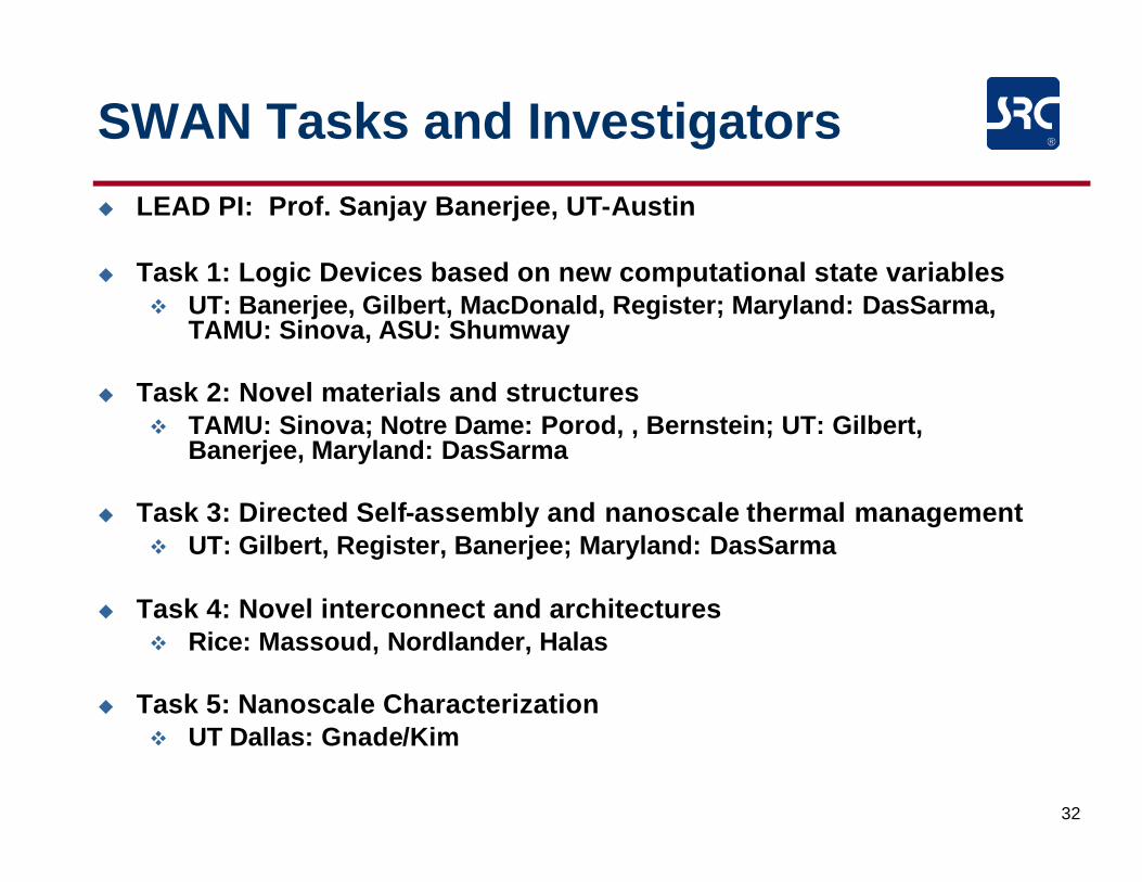
SWAN Team
u Coordinator / Lead PI: Sanjay Banerjee (UT-Austin)
u University of Texas (Austin)v Alan MacDonald, Mathew Gilbert, Frank Register
u University of Texas at Dallasv Bruce Gnade, Moon Kim
u Texas A& M Universityv Jairo Sinova
u Rice Universityv Yehia Massoud, Peter Nordlander, Naomi Halas
u University of Marylandv Sankar DasSarma
u Notre Damev Wolfgang Porod and Gary Bernstein
u Arizona State Universityv John Shumway
u Plan to establish additional relationships with Oak Ridge National Labs, NASA JSC, and potentially other schools / national labs
32
SWAN Tasks and Investigatorsu LEAD PI: Prof. Sanjay Banerjee, UT-Austin
u Task 1: Logic Devices based on new computational state variablesv UT: Banerjee, Gilbert, MacDonald, Register; Maryland: DasSarma,
TAMU: Sinova, ASU: Shumway
u Task 2: Novel materials and structuresv TAMU: Sinova; Notre Dame: Porod, , Bernstein; UT: Gilbert,
Banerjee, Maryland: DasSarma
u Task 3: Directed Self-assembly and nanoscale thermal managementv UT: Gilbert, Register, Banerjee; Maryland: DasSarma
u Task 4: Novel interconnect and architecturesv Rice: Massoud, Nordlander, Halas
u Task 5: Nanoscale Characterizationv UT Dallas: Gnade/Kim
IBM Research
© 2006 IBM Corporation33T.N. Theis to SSSC, October 19, 2006
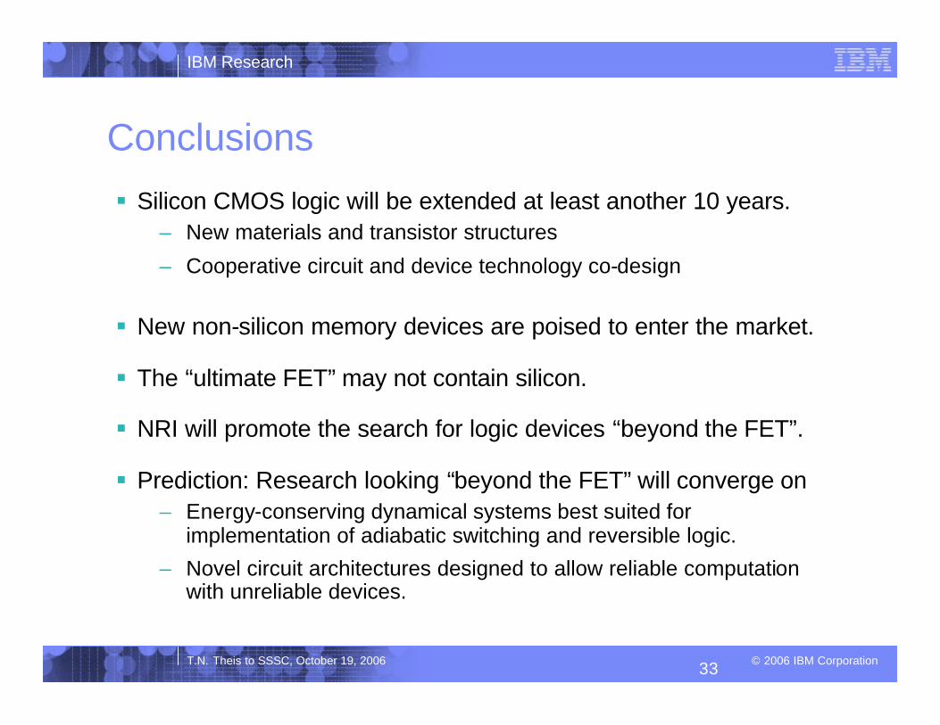
Conclusions
§ Silicon CMOS logic will be extended at least another 10 years. – New materials and transistor structures
– Cooperative circuit and device technology co-design
§ New non-silicon memory devices are poised to enter the market.
§ The “ultimate FET” may not contain silicon.
§ NRI will promote the search for logic devices “beyond the FET”.
§ Prediction: Research looking “beyond the FET” will converge on – Energy-conserving dynamical systems best suited for
implementation of adiabatic switching and reversible logic.
– Novel circuit architectures designed to allow reliable computation with unreliable devices.