Toshiba BiCD Integrated Circuit Silicon Monolithic TB6818FG Sheets/Toshiba PDFs/TB6818FG.… ·...
17
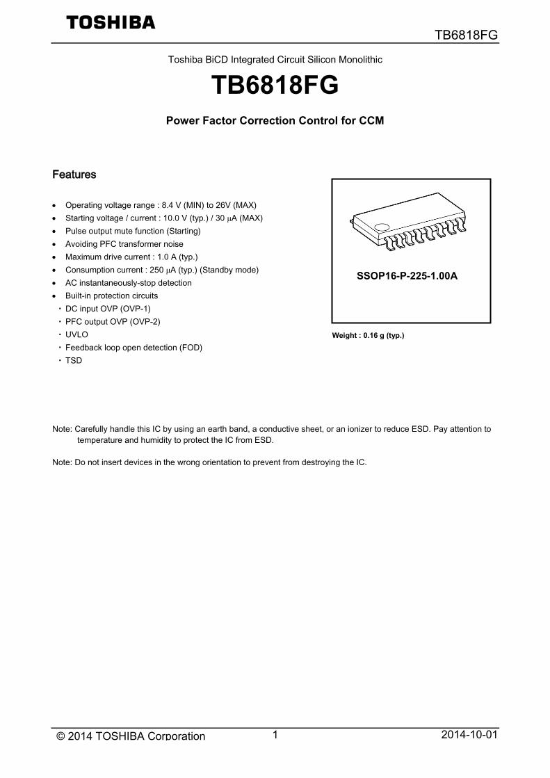
TB6818FG 2014-10-01 1 Toshiba BiCD Integrated Circuit Silicon Monolithic TB6818FG Power Factor Correction Control for CCM Features • Operating voltage range : 8.4 V (MIN) to 26V (MAX) • Starting voltage / current : 10.0 V (typ.) / 30 μA (MAX) • Pulse output mute function (Starting) • Avoiding PFC transformer noise • Maximum drive current : 1.0 A (typ.) • Consumption current : 250 μA (typ.) (Standby mode) • AC instantaneously-stop detection • Built-in protection circuits ・ DC input OVP (OVP-1) ・ PFC output OVP (OVP-2) ・ UVLO ・ Feedback loop open detection (FOD) ・ TSD Note: Carefully handle this IC by using an earth band, a conductive sheet, or an ionizer to reduce ESD. Pay attention to temperature and humidity to protect the IC from ESD. Note: Do not insert devices in the wrong orientation to prevent from destroying the IC. Weight : 0.16 g (typ.) SSOP16-P-225-1.00A © 2014 TOSHIBA Corporation
Transcript of Toshiba BiCD Integrated Circuit Silicon Monolithic TB6818FG Sheets/Toshiba PDFs/TB6818FG.… ·...
TB6818FG
2014-10-01 1
Toshiba BiCD Integrated Circuit Silicon Monolithic
TB6818FG Power Factor Correction Control for CCM
Features • Operating voltage range : 8.4 V (MIN) to 26V (MAX) • Starting voltage / current : 10.0 V (typ.) / 30 μA (MAX) • Pulse output mute function (Starting) • Avoiding PFC transformer noise • Maximum drive current : 1.0 A (typ.) • Consumption current : 250 μA (typ.) (Standby mode) • AC instantaneously-stop detection • Built-in protection circuits ・ DC input OVP (OVP-1) ・ PFC output OVP (OVP-2) ・ UVLO ・ Feedback loop open detection (FOD) ・ TSD
Note: Carefully handle this IC by using an earth band, a conductive sheet, or an ionizer to reduce ESD. Pay attention to
temperature and humidity to protect the IC from ESD. Note: Do not insert devices in the wrong orientation to prevent from destroying the IC.
Weight : 0.16 g (typ.)
SSOP16-P-225-1.00A
© 2014 TOSHIBA Corporation
TB6818FG
2014-10-01 2
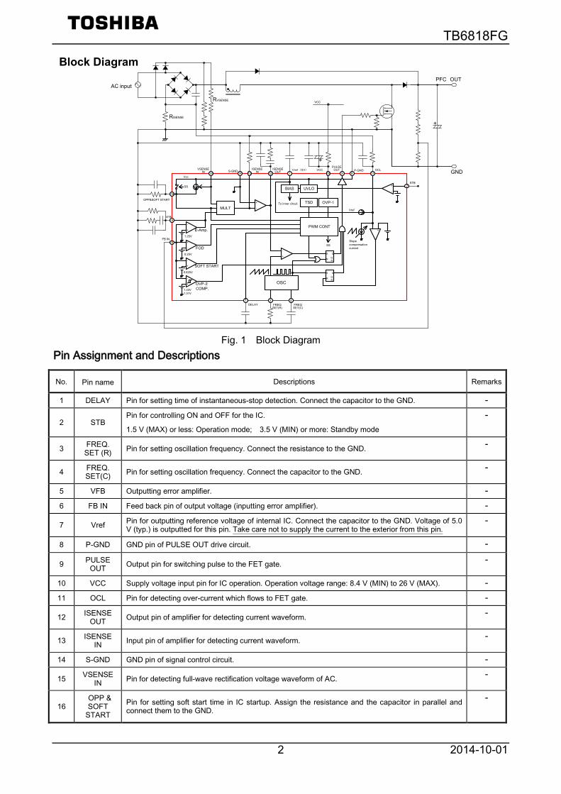
Block Diagram Pin Assignment and Descriptions
No. Pin name Descriptions Remarks
1 DELAY Pin for setting time of instantaneous-stop detection. Connect the capacitor to the GND. -
2 STB Pin for controlling ON and OFF for the IC.
1.5 V (MAX) or less: Operation mode; 3.5 V (MIN) or more: Standby mode
-
3 FREQ. SET (R) Pin for setting oscillation frequency. Connect the resistance to the GND. -
4 FREQ. SET(C) Pin for setting oscillation frequency. Connect the capacitor to the GND. -
5 VFB Outputting error amplifier. -
6 FB IN Feed back pin of output voltage (inputting error amplifier). -
7 Vref Pin for outputting reference voltage of internal IC. Connect the capacitor to the GND. Voltage of 5.0 V (typ.) is outputted for this pin. Take care not to supply the current to the exterior from this pin.
-
8 P-GND GND pin of PULSE OUT drive circuit. -
9 PULSE OUT Output pin for switching pulse to the FET gate. -
10 VCC Supply voltage input pin for IC operation. Operation voltage range: 8.4 V (MIN) to 26 V (MAX). -
11 OCL Pin for detecting over-current which flows to FET gate. -
12 ISENSE OUT Output pin of amplifier for detecting current waveform. -
13 ISENSE IN Input pin of amplifier for detecting current waveform. -
14 S-GND GND pin of signal control circuit. -
15 VSENSE IN Pin for detecting full-wave rectification voltage waveform of AC. -
16 OPP & SOFT
START Pin for setting soft start time in IC startup. Assign the resistance and the capacitor in parallel and connect them to the GND.
-
Fig. 1 Block Diagram
VSENSEIN 15
16
+
-
6
5
OPP&SOFT START
MULT+
-
13 12
OSC
3 4
119
UVLOBIAS
To inner circuit OVP-1
FB IN
VFB
PULSEOUT ISENSE
INISENSE
OUTOCL
FREQSET(R)
FREQSET(C)
2
1DELAY
VCC
Vref
Vcc14
S-GND
Slope compensationcurrent
OVP-2 COMP.
7Vref (5V)
+
-
+-
10
+
-
STB
+
PFC OUT
RVSENSE
+
RISENSE
AC input
GND
TSD
Q
QN
S
R
PWM CONT
Q
QN
S
R
+
-
FOD
+
-
E-Amp.
VCC
+
-
SOFT START
SS
SS
1.25V
0.25V
0.625V
1.33V1.31V
8P-GND
TB6818FG
2014-10-01 3
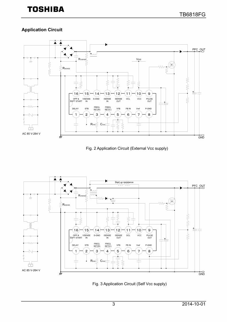
Application Circuit
Fig. 2 Application Circuit (External Vcc supply)
Fig. 3 Application Circuit (Self Vcc supply)
AC 85 V-264 V
PFC OUT
GND
RISENSE
RVSENSE+
PULSE OUT
P-GNDFB INVFB
OCLVSENSEIN
VCCOPP &SOFT START
STB VrefFREQ.SET(R)
65
16 15 1314 12 91011
1 2 3 4 87
DELAY
COSC
+
FREQ.SET(C)
ISENSEIN
ISENSEOUT
ROSC
S-GND
Start up resistance
+
AC 85 V-264 V
PFC OUT
GND
RISENSE
RVSENSE
+
PULSE OUT
P-GNDFB INVFB
OCLVSENSEIN
VCCOPP &SOFT START
STB VrefFREQ.SET(R)
65
16 15 1314 12 91011
1 2 3 4 87
DELAY
COSC
+
FREQ.SET(C)
ISENSEIN
ISENSEOUT
ROSC
S-GND
Vcc
TB6818FG
2014-10-01 4
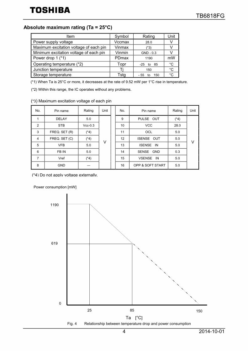
(*3) Maximum excitation voltage of each pin
Power consumption [mW]
(*4) Do not apply voltage externally.
Absolute maximum rating (Ta = 25°C) Item Symbol Rating Unit
Power supply voltage Vccmax 28.0 V Maximum excitation voltage of each pin Vinmax (*3) V Minimum excitation voltage of each pin Vinmin GND - 0.3 V Power drop 1 (*1) PDmax 1190 mW Operating temperature (*2) Topr -25 to 85 °C Junction temperature Tj 150 °C Storage temperature Tstg - 55 to 150 °C
(*1) When Ta is 25°C or more, it decreases at the rate of 9.52 mW per 1°C rise in temperature.
(*2) Within this range, the IC operates without any problems.
No. Pin name Rating Unit
No. Pin name Rating Unit
1 DELAY 5.0
V
9 PULSE OUT (*4)
V
2 STB Vcc-0.3 10 VCC 28.0
3 FREQ. SET (R) (*4) 11 OCL 5.0
4 FREQ. SET (C) (*4) 12 ISENSE OUT 5.0
5 VFB 5.0 13 ISENSE IN 5.0
6 FB IN 5.0 14 SENSE GND 0.3
7 Vref (*4) 15 VSENSE IN 5.0
8 GND ― 16 OPP & SOFT START 5.0
1190
619
Fig. 4 Relationship between temperature drop and power consumption
25 85 150
Ta [°C]
0
TB6818FG
2014-10-01 5
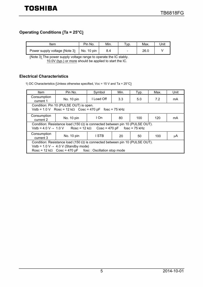
Operating Conditions (Ta = 25°C)
Item Pin No. Min. Typ. Max. Unit
Power supply voltage (Note 3) No. 10 pin 8.4 - 26.0 V
(Note 3) The power supply voltage range to operate the IC stably. 10.0V (typ.) or more should be applied to start the IC.
Electrical Characteristics 1) DC Characteristics (Unless otherwise specified, Vcc = 15 V and Ta = 25°C)
Item Pin No. Symbol Min. Typ. Max. Unit Consumption
current 1 No. 10 pin I Load Off 3.3 5.0 7.2 mA
Condition: Pin 10 (PULSE OUT) is open. Vstb = 1.0 V Rosc = 12 kΩ Cosc = 470 pF fosc = 75 kHz
Consumption current 2 No. 10 pin I On 80 100 120 mA
Condition: Resistance load (150 Ω) is connected between pin 10 (PULSE OUT). Vstb = 4.0 V → 1.0 V Rosc = 12 kΩ Cosc = 470 pF fosc = 75 kHz Consumption
current 3 No. 10 pin I STB 20 50 100 μA
Condition: Resistance load (150 Ω) is connected between pin 10 (PULSE OUT). Vstb = 1.0 V → 4.0 V (Standby mode) Rosc = 12 kΩ Cosc = 470 pF fosc : Oscillation stop mode
TB6818FG
2014-10-01 6
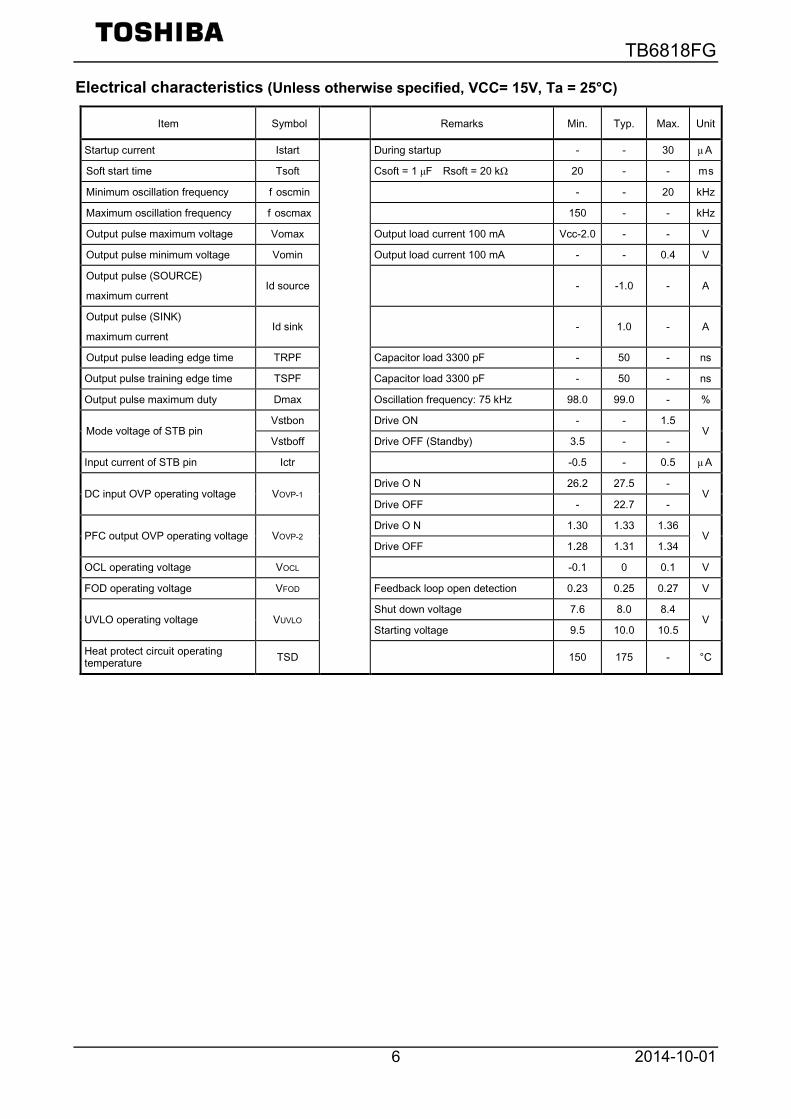
Electrical characteristics (Unless otherwise specified, VCC= 15V, Ta = 25°C)
Item Symbol Remarks Min. Typ. Max. Unit
Startup current Istart
During startup - - 30 μA
Soft start time Tsoft Csoft = 1 μF Rsoft = 20 kΩ 20 - - ms
Minimum oscillation frequency foscmin - - 20 kHz
Maximum oscillation frequency foscmax 150 - - kHz
Output pulse maximum voltage Vomax Output load current 100 mA Vcc-2.0 - - V
Output pulse minimum voltage Vomin Output load current 100 mA - - 0.4 V
Output pulse (SOURCE)
maximum current Id source - -1.0 - A
Output pulse (SINK)
maximum current Id sink - 1.0 - A
Output pulse leading edge time TRPF Capacitor load 3300 pF - 50 - ns
Output pulse training edge time TSPF Capacitor load 3300 pF - 50 - ns
Output pulse maximum duty Dmax Oscillation frequency: 75 kHz 98.0 99.0 - %
Mode voltage of STB pin Vstbon Drive ON - - 1.5
V Vstboff Drive OFF (Standby) 3.5 - -
Input current of STB pin Ictr -0.5 - 0.5 μA
DC input OVP operating voltage VOVP-1 Drive O N 26.2 27.5 -
V Drive OFF - 22.7 -
PFC output OVP operating voltage VOVP-2 Drive O N 1.30 1.33 1.36
V Drive OFF 1.28 1.31 1.34
OCL operating voltage VOCL -0.1 0 0.1 V
FOD operating voltage VFOD Feedback loop open detection 0.23 0.25 0.27 V
UVLO operating voltage VUVLO Shut down voltage 7.6 8.0 8.4
V Starting voltage 9.5 10.0 10.5
Heat protect circuit operating temperature TSD 150 175 - °C
TB6818FG
2014-10-01 7
Pin description (1) DELAY terminal (1 Pin)
It sets the time of instantaneous stop detection. The capacitor should be connected against the ground terminal. When supply of AC voltage stops during operation, the voltage of the OPP & SOFT STATY terminal (16 Pin) starts decreasing. When this voltage decreases below 0.6 V (typ.), the capacitor connected to the DELAY terminal starts charging and the voltage of the DELAY terminal increases from 0 V. At this time, when the supply of AC voltage starts again before the voltage of the DELAY terminal reaches 1.25 V (typ.), the voltage of the OPP & SOFT START terminal (16 Pin) increases. Then when this voltage reaches 0.65 V (typ.), the charged capacitor is discharged and becomes 0 V. In this case, the IC determines that instantaneous stop has recovered and PFC operation remains the same as the state
before stopping the supply of AC voltage. However, if the supply of AC voltage does not start before the voltage of the DELAY terminal reaches 1.25 V (typ.), the
IC determines that it is not an instantaneous stop and forcedly outputs low level for PULSE OUT terminal (9 Pin). Then PFC operation stops. After that, when the supply of AC voltage starts again, the IC starts normal operation. Time of instantaneous stop detection is determined by the formula below.
t (ms) = 50 × C (μF)
(2) STB terminal (2 Pin) It controls ON and OFF of the IC operation.
Operation mode: 1.5 V (MAX) or less Stand by mode: 3.5 V (MIN) or more When the operation switches to standby mode when operating at 10.0 V (typ.) or less, UVLO is released and the IC
operation stops. The IC does not restart by switching operation mode (releasing standby mode). The IC can restart when Vcc is 10.0 V (typ.) or more before it switches to standby mode.
(3) FREQ.SET(R) terminal (3 Pin), FREQ.SET(C) terminal (4 Pin) It sets the oscillation frequency. Resistance (Rosc) is connected to 3 Pin against the ground terminal. Capacitor (Cosc)
is connected to 4 Pin against the ground pin. Resistance of 12 kΩ is recommended. (Refer to the supplemental notes.)
Oscillation frequency (fosc) can be found by the following theoretical formula.
(4) VFB terminal (5 Pin) It outputs the current of error amplifier (trans-conductor amplifier).
The filter is constructed to set the gain 0 dB or less with double frequency of AC input frequency which is superimposed to PFC output, and to have sufficient phase.
(5) FB IN terminal (6 Pin) It is a feedback terminal for PFC output voltage (Input terminal of error amplifier). PFC output is input divided by the resistance. Reference voltage of error amplifier is set 1.25 V (typ.).
This terminal has other functions as follows.
× fosc = 4.24
10 5
Cosc・Rosc
(kHz) Cosc : (pF)
Rosc : (kΩ)
TB6818FG
2014-10-01 8
1) Over voltage detection of PFC output (OVP-2)
When PFC output voltage exceeds 106% of the setting voltage, output signal of PULSE OUT terminal (9 Pin) is forcedly set low and PFC operation stops. The operation restarts when the voltage becomes 105% or less of the setting voltage.
2) Open detection (FOD) of feedback (input of error amplifier) loop When the feedback loop is open, output of PULSE OUT terminal (9 Pin) is set low level and PFC operation stops. 3) Decision whether to perform soft start or not during restart. When the voltage of this terminal is 0.625 V (typ.) or less, the operation restarts with soft start.
(6) Vref terminal (7 Pin) It outputs the reference voltage of the internal IC. The capacitor of 0.1 μF is connected against the ground terminal.
A voltage of 5.0 V (typ.) is output to this terminal. Do not supply current to the exterior from this terminal.
(7) P-GND terminal (8 Pin) GND terminal of driving circuit which outputs PULSE to the PULSE OUT terminal (9 Pin).
(8) PULSE OUT terminal (9 Pin) It outputs switching pulse for FET switching gate.
(9) Vcc terminal (10 Pin) Input terminal of power supply for IC operation.
Operation voltage range is from 8.4 V (MIN) to 26 V (MAX). Be aware that when first powered on, a voltage of 10.0 V (typ.) or more must be applied. (Hysteresis function of UVLO)
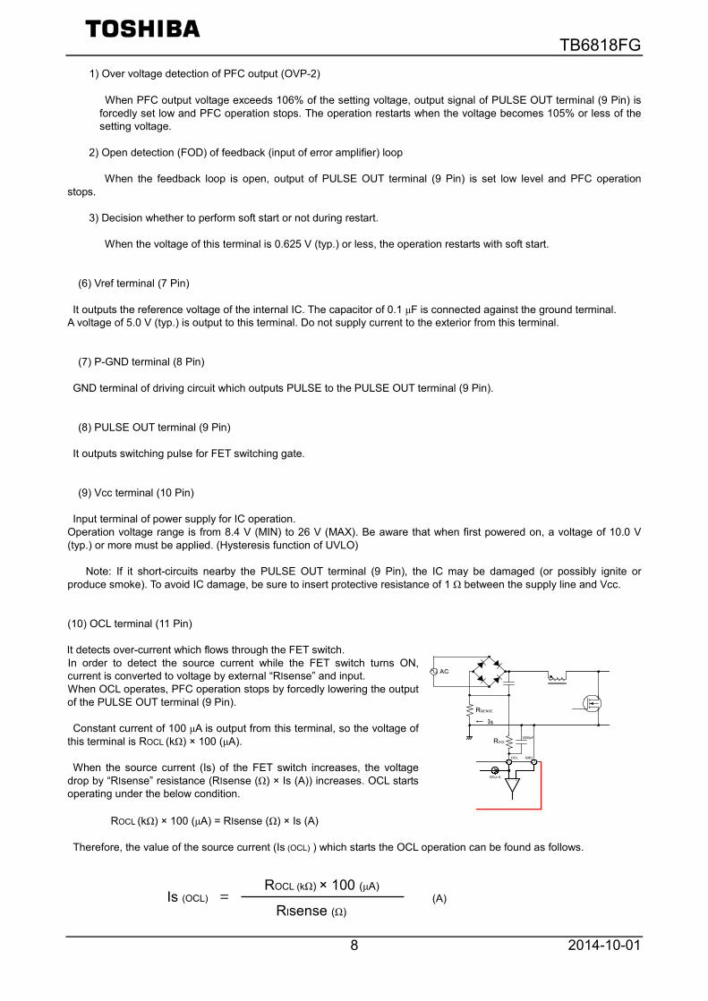
Note: If it short-circuits nearby the PULSE OUT terminal (9 Pin), the IC may be damaged (or possibly ignite or produce smoke). To avoid IC damage, be sure to insert protective resistance of 1 Ω between the supply line and Vcc. (10) OCL terminal (11 Pin) It detects over-current which flows through the FET switch. In order to detect the source current while the FET switch turns ON, current is converted to voltage by external “RIsense” and input. When OCL operates, PFC operation stops by forcedly lowering the output of the PULSE OUT terminal (9 Pin). Constant current of 100 μA is output from this terminal, so the voltage of
this terminal is ROCL (kΩ) × 100 (μA). When the source current (Is) of the FET switch increases, the voltage
drop by “RIsense” resistance (RIsense (Ω) × Is (A)) increases. OCL starts operating under the below condition.
ROCL (kΩ) × 100 (μA) = RIsense (Ω) × Is (A) Therefore, the value of the source current (Is (OCL) ) which starts the OCL operation can be found as follows.
Is (OCL) = ROCL (kΩ) × 100 (μA)
RIsense (Ω) (A)
RISENSE
AC入力
11OCL
+-
ROCL
100μA
1000pF
7
← Is
GND
TB6818FG
2014-10-01 9
OCL detection is invalid for 170 ns (typ.) after the FET switch turns on (output of PULSE OUT terminal (9 Pin) is high
level) to avoid OCL operation introducing errors from needle-like pulse noise generated at the moment the FET switches ON Connect the capacitor of 1000 pF against GND terminal in order to reduce needle-like pulse noise.
(11) ISENSE OUT terminal (12 Pin)
It outputs current (100 μA (MAX) of current detecting amplifier (Trans conductor amplifier). Filter is constructed to set the gain to 0 dB or less around the switching frequency, and to have sufficient phase.
When voltage of this terminal increases, the pulse duty output to the PULSE OUT terminal (9 Pin) becomes narrow. And when the voltage decreases, this duty becomes wide.
(12) ISENSE IN terminal (13 Pin) It inputs current detecting amplifier (Trans conductor amplifier). This terminal is connected to current output of multiple part internally. A maximum current of 200 μA can be output. This
current is converted to voltage by external resistance and inputs to the current detecting amplifier. (13) S-GND terminal (14 Pin) GND terminal for current detecting amplifier (Trans conductor amplifier) and other signal lines. This terminal should be separated from the line of P-GND terminal (8 Pin). If it is connected near the P-GND terminal, PFC may not operate correctly because of the noise.
(14) VSENSE IN terminal (15 Pin) It detects waveform of full-wave commutating voltage of AC voltage.
This terminal should be connected to the voltage line, where AC voltage is commutated with full-wave. And high resistance should be inserted. The voltage is converted to current in the IC and becomes the reference signal for PFC operation. This terminal also detects zero-cross of AC input voltage. In order to detect zero-cross certainly, input waveform of
full-wave commutating voltage should be commutated fully in special circuit, not in the line which is bridge commutated in the main circuit. (Refer to the application circuit) (15) OPP&SOFT START terminal (16 Pin) It sets the soft-start time at IC power on. Resistance and capacitor should be assigned in parallel and are connected
against GND terminal. At IC power on, voltage of this terminal rises to 4.75 V. After that, it falls slowly and settles the constant voltage corresponding to the output load of PFC. During this time, the
pulse duty output to the PULSE OUT terminal (9 Pin) spreads slowly from zero.(soft-start function) This function avoids generating rush current in the FET switch and PFC coil at IC power on.
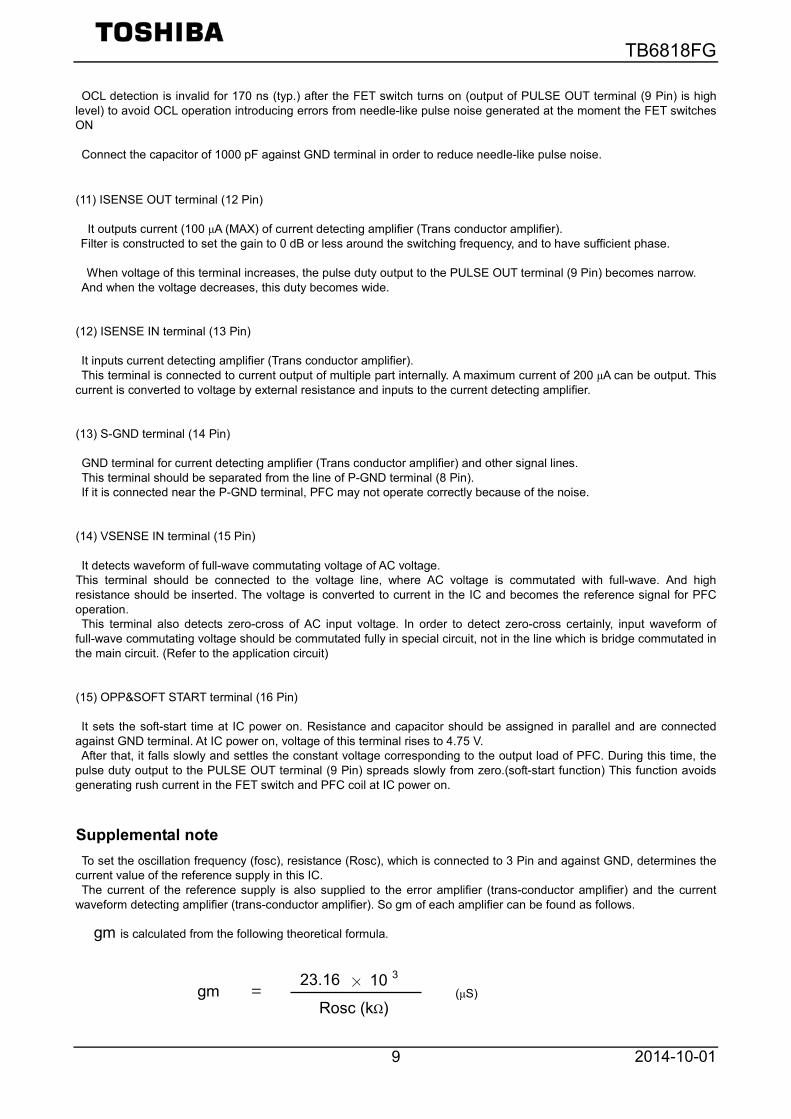
Supplemental note To set the oscillation frequency (fosc), resistance (Rosc), which is connected to 3 Pin and against GND, determines the
current value of the reference supply in this IC. The current of the reference supply is also supplied to the error amplifier (trans-conductor amplifier) and the current
waveform detecting amplifier (trans-conductor amplifier). So gm of each amplifier can be found as follows. gm is calculated from the following theoretical formula.
× gm = 23.16
10 3 Rosc (kΩ)
(μS)
TB6818FG
2014-10-01 10
In applying recommended resistance (12 kΩ), gm of each amplifier is 1.93 (mS). However, if gm is changed please change the resistance. Operation Sequence
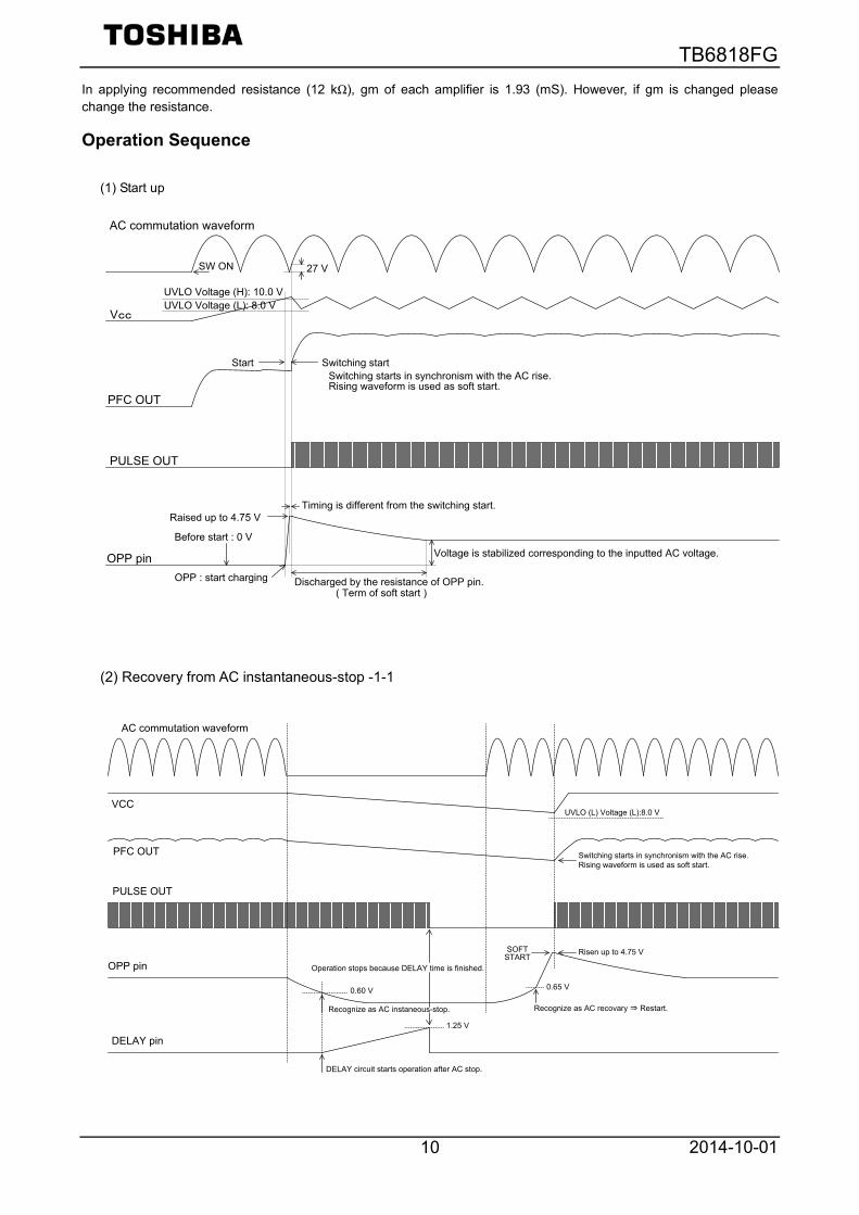
(1) Start up
(2) Recovery from AC instantaneous-stop -1-1
AC commutation waveform
Vcc
PFC OUT
Start
PULSE OUT
Switching starts in synchronism with the AC rise.Rising waveform is used as soft start.
SW ON
Switching start
OPP pinOPP : start charging
Raised up to 4.75 V
Discharged by the resistance of OPP pin. ( Term of soft start )
Timing is different from the switching start.
Voltage is stabilized corresponding to the inputted AC voltage.Before start : 0 V
27 V
UVLO Voltage (H): 10.0 VUVLO Voltage (L): 8.0 V
Switching starts in synchronism with the AC rise.Rising waveform is used as soft start.
AC commutation waveform
VCC
PFC OUT
OPP pinRisen up to 4.75 V
0.60 V 0.65 V
1.25 V
DELAY pin
Recognize as AC instaneous-stop. Recognize as AC recovary ⇒ Restart.
SOFTSTART
Operation stops because DELAY time is finished.
DELAY circuit starts operation after AC stop.
UVLO (L) Voltage (L):8.0 V
PULSE OUT
TB6818FG
2014-10-01 11
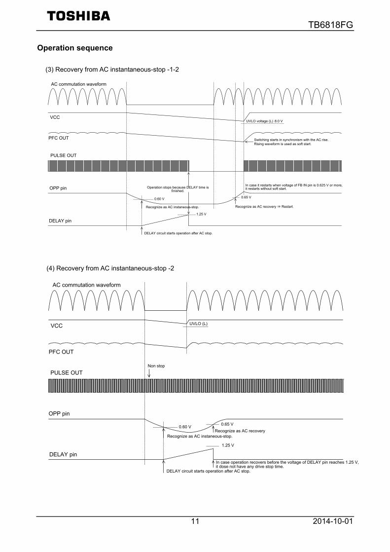
Operation sequence
(3) Recovery from AC instantaneous-stop -1-2
(4) Recovery from AC instantaneous-stop -2
Switching starts in synchronism with the AC rise.Rising waveform is used as soft start.
VCC
PFC OUT
PULSE OUT
OPP pin
0.60 V 0.65 V
1.25 V
DELAY pin
UVLO voltage (L):8.0 V
AC commutation waveform
Recognize as AC instaneous-stop.
DELAY circuit starts operation after AC stop.
Operation stops because DELAY time is finished.
Recognize as AC recovery ⇒ Restart.
In case it restarts when voltage of FB IN pin is 0.625 V or more, it restarts without soft start.
VCC
PFC OUT
OPP pin
0.60 V 0.65 V
1.25 V
DELAY pinIn case operation recovers before the voltage of DELAY pin reaches 1.25 V, it dose not have any drive stop time.
Non stop
UVLO (L)
AC commutation waveform
Recognize as AC instaneous-stop.Recognize as AC recovery
DELAY circuit starts operation after AC stop.
PULSE OUT
TB6818FG
2014-10-01 12
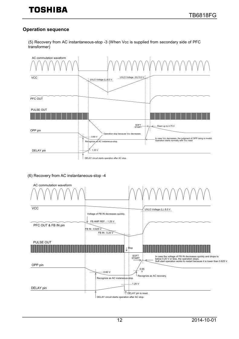
Operation sequence
(5) Recovery from AC instantaneous-stop -3 (When Vcc is supplied from secondary side of PFC transformer)
(6) Recovery from AC instantaneous-stop -4
VCC
0.60 V0.65
V
1.25 V
SOFTSTART
PULSE OUT
UVLO Voltage (L):8.0 V
AC commutation waveform
PFC OUT & FB IN pin
OPP pin
DELAY pin
Voltage of FB IN decreases quickly.
FB AMP REF. : 1.25 V
FB IN : 0.625 VFB IN : 0.25 V
In case the voltage of FB IN decreases quickly and drops to below 0.25 V or less, the operation stops.Soft start operation works to restart because it is lower than 0.625 V.
Recognize as AC recovery.
DELAY pin is reset.DELAY circuit starts operation after AC stop.
Stop
Recognize as AC instaneous-stop.
VCC
PFC OUT
OPP pin
UVLO Voltage (L):8.0 V
0.60 V
1.25 VDELAY pin
SOFTSTART
Operation stop because Vcc decreases
UVLO Voltage (H):10.0 V
In case Vcc decreases, the judgment of OPP rising is invalid.Operation starts normally with Vcc rised
DELAY circuit starts operation after AC stop.
Recognize as AC instaneous-stop.
Risen up to 4.75 V
AC commutation waveform
PULSE OUT
TB6818FG
2014-10-01 13
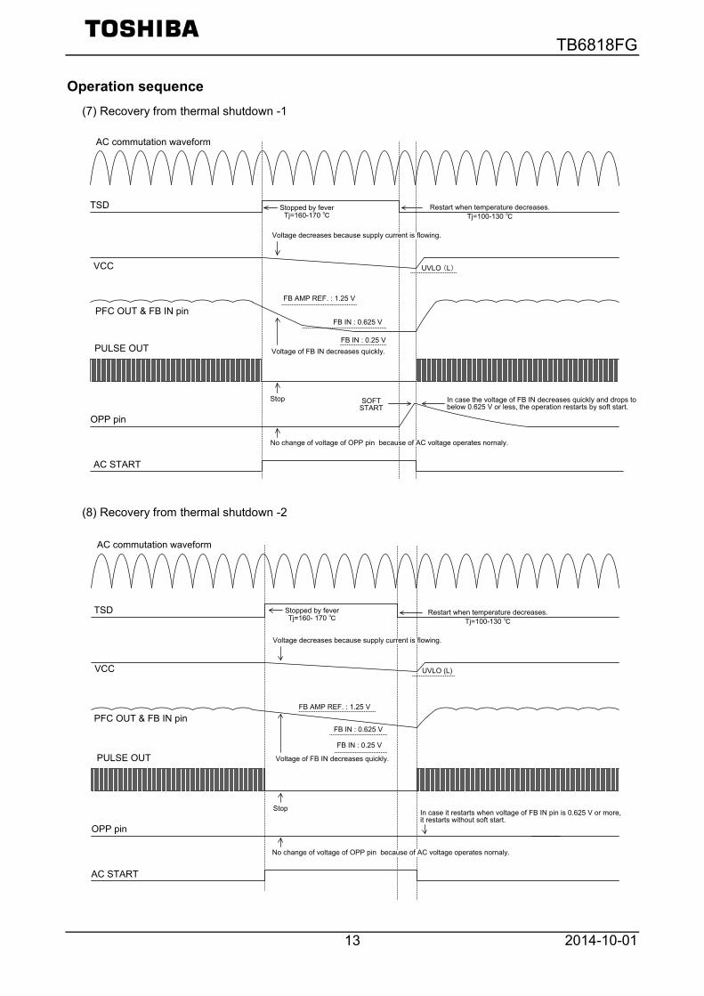
Operation sequence
(7) Recovery from thermal shutdown -1
(8) Recovery from thermal shutdown -2
VCC
PFC OUT & FB IN pin
OPP pin
UVLO (L)
No change of voltage of OPP pin because of AC voltage operates nornaly.
SOFTSTART
Stop
TSD Stopped by feverTj=160-170 ℃
Restart when temperature decreases.Tj=100-130 ℃
Voltage decreases because supply current is flowing.
AC START
FB AMP REF. : 1.25 V
FB IN : 0.625 V
FB IN : 0.25 VVoltage of FB IN decreases quickly.
In case the voltage of FB IN decreases quickly and drops to below 0.625 V or less, the operation restarts by soft start.
AC commutation waveform
PULSE OUT
VCC
PFC OUT & FB IN pin
OPP pin
UVLO (L)
Stop
TSD
In case it restarts when voltage of FB IN pin is 0.625 V or more, it restarts without soft start.
AC START
Stopped by feverTj=160- 170 ℃
Voltage decreases because supply current is flowing.
FB AMP REF. : 1.25 V
FB IN : 0.625 V
FB IN : 0.25 V
Voltage of FB IN decreases quickly.
Restart when temperature decreases.Tj=100-130 ℃
AC commutation waveform
No change of voltage of OPP pin because of AC voltage operates nornaly.
PULSE OUT
TB6818FG
2014-10-01 14
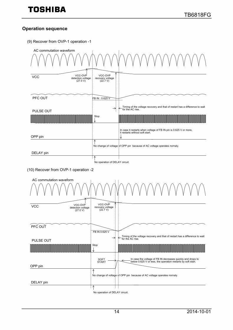
Operation sequence
(9) Recover from OVP-1 operation -1
(10) Recover from OVP-1 operation -2
VCC
PFC OUT
OPP pin
DELAY pin
Stop
VCC-OVP detection voltage
(27.0 V)
Timing of the voltage recovery and that of restart has a difference to wait for the AC rise.
VCC-OVP recovery voltage
(22.7 V)
FB IN : 0.625 V
AC commutation waveform
In case it restarts when voltage of FB IN pin is 0.625 V or more, it restarts without soft start.
No change of voltage of OPP pin because of AC voltage operates nornaly.
No operation of DELAY circuit.
PULSE OUT
VCC
PFC OUT
OPP pin
DELAY pin
Stop
VCC-OVP detection voltage
(27.0 V)
VCC-OVP recovery voltage
(22.7 V)
FB IN 0.625 V
Timing of the voltage recovery and that of restart has a difference to wait for the AC rise.
No change of voltage of OPP pin because of AC voltage operates nornaly.
No operation of DELAY circuit.
In case the voltage of FB IN decreases quickly and drops to below 0.625 V or less, the operation restarts by soft start.
AC commutation waveform
SOFTSTART
PULSE OUT
TB6818FG
2014-10-01 15
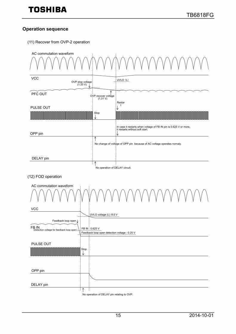
Operation sequence
(11) Recover from OVP-2 operation
(12) FOD operation
VCC
PFC OUT
OPP pin
DELAY pin
No operation of DELAY circuit.
Stop
OVP stop voltage (1.33 V)
OVP recover voltage (1.31 V)
Restart
UVLO (L)
In case it restarts when voltage of FB IN pin is 0.625 V or more, it restarts without soft start.
No change of voltage of OPP pin because of AC voltage operates nornaly.
AC commutation waveform
PULSE OUT
OPP pin
DELAY pin
FB IN
VCC
PULSE OUT
UVLO voltage (L):8.0 V
Feedback loop open
(Detection voltage for feedback loop open)Feedback loop open detection voltage : 0.25 V
Stop
FB IN : 0.625 V
No operation of DELAY pin relating to OVP.
AC commutation waveform
TB6818FG
2014-10-01 16
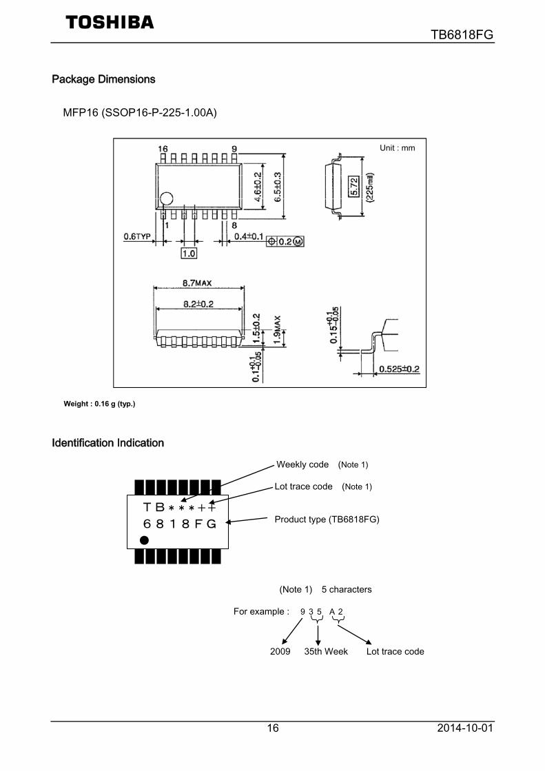
Package Dimensions
MFP16 (SSOP16-P-225-1.00A)
Identification Indication
Weekly code (Note 1) Lot trace code (Note 1) Product type (TB6818FG)
(Note 1) 5 characters
For example : 935 A2
2009 35th Week Lot trace code
TB***++
6818FG
●
Unit : mm
Weight : 0.16 g (typ.)
TB6818FG
2014-10-01 17
RESTRICTIONS ON PRODUCT USE
• Toshiba Corporation, and its subsidiaries and affiliates (collectively "TOSHIBA"), reserve the right to make changes to the information in this document, and related hardware, software and systems (collectively "Product") without notice.
• This document and any information herein may not be reproduced without prior written permission from TOSHIBA. Even with TOSHIBA's written permission, reproduction is permissible only if reproduction is without alteration/omission.
• Though TOSHIBA works continually to improve Product's quality and reliability, Product can malfunction or fail. Customers are responsible for complying with safety standards and for providing adequate designs and safeguards for their hardware, software and systems which minimize risk and avoid situations in which a malfunction or failure of Product could cause loss of human life, bodily injury or damage to property, including data loss or corruption. Before customers use the Product, create designs including the Product, or incorporate the Product into their own applications, customers must also refer to and comply with (a) the latest versions of all relevant TOSHIBA information, including without limitation, this document, the specifications, the data sheets and application notes for Product and the precautions and conditions set forth in the "TOSHIBA Semiconductor Reliability Handbook" and (b) the instructions for the application with which the Product will be used with or for. Customers are solely responsible for all aspects of their own product design or applications, including but not limited to (a) determining the appropriateness of the use of this Product in such design or applications; (b) evaluating and determining the applicability of any information contained in this document, or in charts, diagrams, programs, algorithms, sample application circuits, or any other referenced documents; and (c) validating all operating parameters for such designs and applications. TOSHIBA ASSUMES NO LIABILITY FOR CUSTOMERS' PRODUCT DESIGN OR APPLICATIONS.
• PRODUCT IS NEITHER INTENDED NOR WARRANTED FOR USE IN EQUIPMENTS OR SYSTEMS THAT REQUIRE EXTRAORDINARILY HIGH LEVELS OF QUALITY AND/OR RELIABILITY, AND/OR A MALFUNCTION OR FAILURE OF WHICH MAY CAUSE LOSS OF HUMAN LIFE, BODILY INJURY, SERIOUS PROPERTY DAMAGE AND/OR SERIOUS PUBLIC IMPACT ("UNINTENDED USE"). Except for specific applications as expressly stated in this document, Unintended Use includes, without limitation, equipment used in nuclear facilities, equipment used in the aerospace industry, medical equipment, equipment used for automobiles, trains, ships and other transportation, traffic signaling equipment, equipment used to control combustions or explosions, safety devices, elevators and escalators, devices related to electric power, and equipment used in finance-related fields. IF YOU USE PRODUCT FOR UNINTENDED USE, TOSHIBA ASSUMES NO LIABILITY FOR PRODUCT. For details, please contact your TOSHIBA sales representative.
• Do not disassemble, analyze, reverse-engineer, alter, modify, translate or copy Product, whether in whole or in part.
• Product shall not be used for or incorporated into any products or systems whose manufacture, use, or sale is prohibited under any applicable laws or regulations.
• The information contained herein is presented only as guidance for Product use. No responsibility is assumed by TOSHIBA for any infringement of patents or any other intellectual property rights of third parties that may result from the use of Product. No license to any intellectual property right is granted by this document, whether express or implied, by estoppel or otherwise.
• ABSENT A WRITTEN SIGNED AGREEMENT, EXCEPT AS PROVIDED IN THE RELEVANT TERMS AND CONDITIONS OF SALE FOR PRODUCT, AND TO THE MAXIMUM EXTENT ALLOWABLE BY LAW, TOSHIBA (1) ASSUMES NO LIABILITY WHATSOEVER, INCLUDING WITHOUT LIMITATION, INDIRECT, CONSEQUENTIAL, SPECIAL, OR INCIDENTAL DAMAGES OR LOSS, INCLUDING WITHOUT LIMITATION, LOSS OF PROFITS, LOSS OF OPPORTUNITIES, BUSINESS INTERRUPTION AND LOSS OF DATA, AND (2) DISCLAIMS ANY AND ALL EXPRESS OR IMPLIED WARRANTIES AND CONDITIONS RELATED TO SALE, USE OF PRODUCT, OR INFORMATION, INCLUDING WARRANTIES OR CONDITIONS OF MERCHANTABILITY, FITNESS FOR A PARTICULAR PURPOSE, ACCURACY OF INFORMATION, OR NONINFRINGEMENT.
• Do not use or otherwise make available Product or related software or technology for any military purposes, including without limitation, for the design, development, use, stockpiling or manufacturing of nuclear, chemical, or biological weapons or missile technology products (mass destruction weapons). Product and related software and technology may be controlled under the applicable export laws and regulations including, without limitation, the Japanese Foreign Exchange and Foreign Trade Law and the U.S. Export Administration Regulations. Export and re-export of Product or related software or technology are strictly prohibited except in compliance with all applicable export laws and regulations.
• Please contact your TOSHIBA sales representative for details as to environmental matters such as the RoHS compatibility of Product. Please use Product in compliance with all applicable laws and regulations that regulate the inclusion or use of controlled substances, including without limitation, the EU RoHS Directive. TOSHIBA ASSUMES NO LIABILITY FOR DAMAGES OR LOSSES OCCURRING AS A RESULT OF NONCOMPLIANCE WITH APPLICABLE LAWS AND REGULATIONS.