Surface Stability of SrNbO Grown by Hybrid Molecular Beam ...
14
Surface Stability of SrNbO 3+δ Grown by Hybrid Molecular Beam Epitaxy Suresh Thapa 1 , Sydney Provence 1 , Steve M. Heald 2 , Marcelo A. Kuroda 1 , and Ryan B. Comes 1 1 Department of Physics, Auburn University, Auburn, AL 36830, USA 2 Advanced Photon Source, Argonne National Laboratory, Argonne, IL 60439, USA Abstract: 4d transition metal oxides have emerged as promising materials for numerous applications including high mobility electronics. SrNbO 3 is one such candidate material, serving as a good donor material in interfacial oxide systems and exhibiting high electron mobility in ultrathin films. However, its synthesis is challenging due to the metastable nature of the d 1 Nb 4+ cation and the limitations in the delivery of refractory Nb. To date, films have been grown primarily by pulsed laser deposition (PLD), but development of a means to grow and stabilize the material via molecular beam epitaxy (MBE) would enable studies of interfacial phenomena and multilayer structures that may be challenging by PLD. To that end, SrNbO 3 thin films were grown using hybrid MBE for the first time using a tris(diethalamido)(tert-butylimido) niobium precursor for Nb and an elemental Sr source on GdScO 3 substrates. Varying thicknesses of insulating SrHfO 3 capping layers were deposited using a hafnium tert-butoxide precursor for Hf on top of SrNbO 3 films to preserve the metastable surface. Grown films were transferred in vacuo for X-ray photoelectron spectroscopy to quantify elemental composition, density of states at the Fermi energy, and Nb oxidation state. Ex situ studies by X-ray absorption near edge spectra illustrates the SrHfO 3 capping plays an important role in preserving the Nb 4d 1 metastable charge state in atmospheric conditions. Introduction: For two decades, the study of two dimensional electron gas (2DEGs) in complex metal oxides has rapidly increased after its observation at the LaAlO 3 (LAO)/SrTiO 3 (STO) interface [1]. This interesting phenomenon has driven ongoing research for two decades, opening the door for complex oxide interfaces as strong contenders for high carrier concentrations and high electron mobility. Oxide 2DEGs [2,3] offer unique opportunities compared to traditional semiconductor ones as they may exhibit strong spin-orbit coupling along with possibility of harnessing high carrier concentrations [citation?]. The search for a good donor oxide is a great challenge when building a high carrier concentration and mobility in oxides interface for high-speed electronics. Isoelectronic to the SrVO 3 , SrNbO 3 (SNO) has a d 1 electronic configuration and a simple cubic perovskite structure with lattice parameter between 4.0 and 4.1 Å [4]. The band diagram of SNO reveals the Nb 4d t 2g bands crossing the Fermi level, indicating its metallic nature, whereas the low work function makes SNO stand out as a suitable donor [5], as previously reported in density functional theory (DFT) studies on SNO/STO heterostructures [6]. SNO has also been discovered as the first plasmonic photocatalyst metallic oxide, which opens a door for new family of photocatalytic materials [7]. Studies have also examined the material for use as a plasmonic transparent conducting material due to the large band gap between the O 2p and Nb 4d bands [8–10]. Recent results have also shown that epitaxial strain in SNO films can break cubic symmetry to produce a semimetallic tetragonal phase with extremely high mobility and an observed Berry phase that make it promising for quantum materials applications [11]. Large linear magnetoresistances of ~10 5 % and mobilities of 80,000 cm 2 /V-s have also recently been reported in SNO/STO heterostructures [12], suggesting that the material holds exceptional promise in topological and quantum materials research. Despite the great potential of SNO for interfacial charge transfer and topological phenomena as well as its photocatalytic properties, limited work has been carried out in synthesis of pristine SNO thin films. There are numerous unanswered questions on basic properties of SNO, its surface stability, and its applications
Transcript of Surface Stability of SrNbO Grown by Hybrid Molecular Beam ...
Surface Stability of SrNbO3+δ Grown by Hybrid Molecular Beam Epitaxy
Suresh Thapa1, Sydney Provence1, Steve M. Heald2, Marcelo A. Kuroda1, and Ryan B. Comes1
1Department of Physics, Auburn University, Auburn, AL 36830, USA 2Advanced Photon Source, Argonne National Laboratory, Argonne, IL 60439, USA
Abstract:
4d transition metal oxides have emerged as promising materials for numerous applications including high
mobility electronics. SrNbO3 is one such candidate material, serving as a good donor material in interfacial
oxide systems and exhibiting high electron mobility in ultrathin films. However, its synthesis is challenging
due to the metastable nature of the d1 Nb4+ cation and the limitations in the delivery of refractory Nb. To
date, films have been grown primarily by pulsed laser deposition (PLD), but development of a means to
grow and stabilize the material via molecular beam epitaxy (MBE) would enable studies of interfacial
phenomena and multilayer structures that may be challenging by PLD. To that end, SrNbO3 thin films were
grown using hybrid MBE for the first time using a tris(diethalamido)(tert-butylimido) niobium precursor
for Nb and an elemental Sr source on GdScO3 substrates. Varying thicknesses of insulating SrHfO3 capping
layers were deposited using a hafnium tert-butoxide precursor for Hf on top of SrNbO3 films to preserve
the metastable surface. Grown films were transferred in vacuo for X-ray photoelectron spectroscopy to
quantify elemental composition, density of states at the Fermi energy, and Nb oxidation state. Ex situ studies
by X-ray absorption near edge spectra illustrates the SrHfO3 capping plays an important role in preserving
the Nb 4d1 metastable charge state in atmospheric conditions.
Introduction:
For two decades, the study of two dimensional electron gas (2DEGs) in complex metal oxides has rapidly
increased after its observation at the LaAlO3 (LAO)/SrTiO3 (STO) interface [1]. This interesting
phenomenon has driven ongoing research for two decades, opening the door for complex oxide interfaces
as strong contenders for high carrier concentrations and high electron mobility. Oxide 2DEGs [2,3] offer
unique opportunities compared to traditional semiconductor ones as they may exhibit strong spin-orbit
coupling along with possibility of harnessing high carrier concentrations [citation?]. The search for a good
donor oxide is a great challenge when building a high carrier concentration and mobility in oxides interface
for high-speed electronics. Isoelectronic to the SrVO3, SrNbO3 (SNO) has a d1 electronic configuration and
a simple cubic perovskite structure with lattice parameter between 4.0 and 4.1 Å [4]. The band diagram of
SNO reveals the Nb 4d t2g bands crossing the Fermi level, indicating its metallic nature, whereas the low
work function makes SNO stand out as a suitable donor [5], as previously reported in density functional
theory (DFT) studies on SNO/STO heterostructures [6]. SNO has also been discovered as the first
plasmonic photocatalyst metallic oxide, which opens a door for new family of photocatalytic materials [7].
Studies have also examined the material for use as a plasmonic transparent conducting material due to the
large band gap between the O 2p and Nb 4d bands [8–10]. Recent results have also shown that epitaxial
strain in SNO films can break cubic symmetry to produce a semimetallic tetragonal phase with extremely
high mobility and an observed Berry phase that make it promising for quantum materials applications [11].
Large linear magnetoresistances of ~105 % and mobilities of 80,000 cm2/V-s have also recently been
reported in SNO/STO heterostructures [12], suggesting that the material holds exceptional promise in
topological and quantum materials research.
Despite the great potential of SNO for interfacial charge transfer and topological phenomena as well as its
photocatalytic properties, limited work has been carried out in synthesis of pristine SNO thin films. There
are numerous unanswered questions on basic properties of SNO, its surface stability, and its applications

for interfacial engineering of emergent materials properties. Previous reports on SNO thin film growth have
employed pulsed laser deposition (PLD) [10–15] and sputtering [8,9]. There are no reports of MBE
synthesis of SNO, though NbO2 [16] and Nb-doped STO [17] have been synthesized by MBE using an
electron-beam evaporation source. In particular, previous work [14] examining the electronic band structure
using in situ angle-resolved photoemission spectroscopy (ARPES) measurements provided insights into
SNO thin films and verified the metallic character of SNO experimentally. However, this work also showed
a significant excess of Nb5+ atomic valence relative to the expected 4+ charge state, which suppressed the
spectral weight of electronic states near the Fermi level. These results were attributed to surface Nb5+ states
due to either Sr vacancies or formation of Nb2O5. However, adsorption of excess oxygen is also an
alternative mechanism to accommodate the conversion from metastable Nb4+ to the stable d0 Nb5+ state
through the formation of a Sr2Nb2O7 phase [15,18,19]. Similar results have also been observed in d1 rare
earth titanates [20,21] and SrVO3 [16] previously. Clearly, understanding and controlling the valence of Nb
ions in SNO films is important to the development of interfacial heterostructures that leverage the d1
electronic configuration and propensity of SNO to donate electrons to neighboring materials [11,12].
One of the most likely approaches to preserve metastable SNO is by capping films with an alternative oxide
with greater atmospheric stability. To date, there have been no reports of suitable capping layers for SNO.
However, such an approach has been employed for DyTiO3 films via a LaAlO3 cap, which significantly
enhanced the ratio of metastable Ti3+ vs d0 Ti4+ [21]. A perovskite oxide with a higher band gap, matching
A site cation, and one that does not accept electrons from SNO would be a reasonable choice as a capping
layer. SrHfO3 (SHO) is well known for its large band gap of 6.07 eV [22] and is expected to have a band
alignment that prevents electron transfer, [5] which makes it an ideal perovskite oxide for capping in this
system. However, the delivery of both Nb and Hf is highly challenging due to their refractory natures. To
overcome this discrepancy, the hybrid molecular beam epitaxy technique opens opportunities for Nb and
Hf to be supplied as metal organic precursors.
In addition to PLD, molecular beam epitaxy (MBE) is well established for the synthesis of various metal
oxides over the last three decades. However, repeatable growth of a complex metal oxide incorporating
refractory metal cations with stoichiometric control by traditional MBE is extra challenging as they lack
the adsorption-controlled growth window. In the past decade, hybrid MBE (hMBE) has been established
as a state-of-the-art technique to grow complex metal oxides where refractory metals are supplied through
a metal organic precursor and the A-site cation is supplied as a metallic source [23]. The hMBE technique
is highly efficient in delivering low vapor pressure and refractory metals for repeatable growth of large
varieties of high quality metal oxides such as SrVO3 [24] , BaSnO3 [25] , and SrTiO3 (STO) [26,27] with
improved stoichiometric control compared to the traditional MBE growth. This approach offers significant
advantages over deposition with an electron-beam evaporator in an MBE, where achieving repeatable and
stable growth conditions can be a challenge.
Selection of precursor becomes highly important in perovskite oxides growth involving refractory metals
as they determine the delivery of B-site cation. Previous reports [28,29] on synthesis of Nb2O5 by atomic
layer deposition (ALD) suggest that niobium ethoxide (NbOEt) and tris(diethalamido)(tert-butylimido)
niobium (TDTBN) are the most suitable precursors as a Nb precursor. However, NbOEt decomposition
rather than evaporation in its molecular form has been reported due to significantly lower vapor pressure
of NbOEt compared to TDTBN [29]. TDTBN was liquid at room temperature and successfully evaporated
for ALD at 65 °C using open boats due to the low vapor pressure of the precursor. Recent work has shown
both thermal and plasma-enhanced ALD of Nb2O5 using TDTBN [30]. In the case of thermal ALD,
significant amounts of Nb4+ ions were observed in the films grown at high temperatures, likely because,
unlike NbOEt, TDTBN contains no oxygen atoms in the molecule. The chemical structure of the molecule
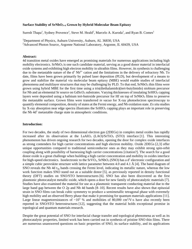
is shown in Figure 1. The lack of oxygen in the TDTBN precursor may afford greater control over the
overall oxidation of the film because the delivery of molecular O2 and oxygen plasma can be tuned to vary
the oxygen chemical potential in the system over a wide range.
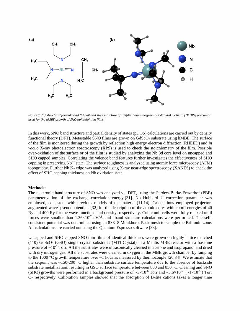
Figure 1: (a) Structural formula and (b) ball and stick structure of tris(diethalamido)(tert-butylimido) niobium (TDTBN) precursor used for the hMBE growth of SNO epitaxial thin films.
In this work, SNO band structure and partial density of states (pDOS) calculations are carried out by density
functional theory (DFT). Metastable SNO films are grown on GdScO3 substrate using hMBE. The surface
of the film is monitored during the growth by reflection high energy electron diffraction (RHEED) and in
vacuo X-ray photoelectron spectroscopy (XPS) is used to check the stoichiometry of the film. Possible
over-oxidation of the surface or of the film is studied by analyzing the Nb 3d core level on uncapped and
SHO capped samples. Correlating the valence band features further investigates the effectiveness of SHO
capping in preserving Nb4+ state. The surface roughness is analyzed using atomic force microscopy (AFM)
topography. Further Nb K- edge was analyzed using X-ray near-edge spectroscopy (XANES) to check the
effect of SHO capping thickness on Nb oxidation state.
Methods:
The electronic band structure of SNO was analyzed via DFT, using the Perdew-Burke-Ernzerhof (PBE)
parameterization of the exchange-correlation energy [31]. No Hubbard U correction parameter was
employed, consistent with previous models of the material [11,14]. Calculations employed projector-
augmented-wave pseudopotentials [32] for the description of the atomic cores with cutoff energies of 40
Ry and 400 Ry for the wave functions and density, respectively. Cubic unit cells were fully relaxed until
forces were smaller than 1.36×10⁻⁷ eV/Å and band structure calculations were performed. The self-
consistent potential was determined using an 8×8×8 Monkhorst-Pack mesh to sample the Brillouin zone.
All calculations are carried out using the Quantum Espresso software [33].
Uncapped and SHO capped SNO thin films of identical thickness were grown on highly lattice matched
(110) GdScO3 (GSO) single crystal substrates (MTI Crystal) in a Mantis MBE reactor with a baseline
pressure of ~10-9 Torr. All the substrates were ultrasonically cleaned in acetone and isopropanol and dried
with dry nitrogen gas. All the substrates were cleaned in oxygen in the MBE growth chamber by ramping
to the 1000 °C growth temperature over ~1 hour as measured by thermocouple [26,34]. We estimate that
the setpoint was ~150-200 °C higher than substrate surface temperature due to the absence of backside
substrate metallization, resulting in GSO surface temperature between 800 and 850 °C. Cleaning and SNO
(SHO) growths were performed in a background pressure of ~3×10⁻⁶ Torr and ~3.6×10⁻⁶ (~1×10⁻⁵ ) Torr
O2 respectively. Calibration samples showed that the absorption of B-site cations takes a longer time
compared to low flux of A-site cation. To control the exposure duration, alternate shutter deposition is
applied to supply A and B-site cations in both SNO and SHO deposition. For the metalorganic sources, a
pneumatic ALD valve (Swagelok 316L) is used to isolate the sources when they are not depositing and
serves as the shutter for the deposition.
A series of uncapped and varying SHO thickness capped SNO samples were grown where Sr and
tris(diethalamido)(tert-butylimido) niobium (TDTBN) fluxes were held fixed. The flux of SrO is measured
by quartz crystal microbalance (QCM) in Å/sec. Strontium (99.99%, Sigma-Aldrich, USA) was supplied
through low temperature effusion cell. The Sr flux was calibrated using QCM under oxygen environment
with measured chamber pressure of 3×10⁻⁶ Torr. Niobium was supplied through a gas source using the
TDTBN metal-organic precursor (99.99%, Sigma-Aldrich, USA) from a bubbler connected to the growth
chamber using the ALD pneumatic valve and a heated gas injector source (E-Science, USA). No carrier gas
was used. The gas injector was held at 90 °C using a PID controller and the bubbler at 73 °C through
external heating tape and a PID controller. While the vapor pressure was not measured directly, the chamber
pressure showed only marginal changes (~1%) upon valve actuation, suggesting that the vapor pressure is
in the range of 1-100 mTorr that is commonly employed for hMBE using a pressure-control feedback
system [23]. This configuration can thus be thought of as a modified metal-organic evaporation source that
replicates the capabilities of a low temperature effusion cell for organic molecules.
The growth chamber shroud walls were maintained at -30 °C via a closed loop chiller and low temperature
fluid (Syltherm XLT, Dow Chemical) to reduce the background water vapor pressure from the dissociated
TDTBN molecules. The chamber pressure measured by cold cathode gauge generally increases and reaches
one unit higher at 10-6 Torr for the first 5-10 secs as the TDTBN supply valve is opened before stabilizing
due to the dissociated and unreacted TDTBN injected into the system. O2 flow is turned off for uncapped
sample during cool down to minimize over-oxidation of the film or of the surface of the film. Right after
the SNO deposition, the hafnium tert-butoxide (HTB) flux is calibrated and varying thickness of SHO
capping layers were deposited turning on O2 flow with measured chamber pressure of ~1×10⁻⁵ Torr O2.
Hafnium was supplied through a gas source using a metalorganic precursor, HTB (99.999%, Sigma-
Aldrich, USA) from a bubbler connected to the growth chamber without carrier gas and controlled using a
traditional pressure-control feedback loop [23,35]. Here we have presented four representative samples
among all the samples including one uncapped and three capped annotated as thin (2 unit cells, ~0.8 nm),
medium (3 unit cells, ~1.2 nm), and thick (4 unit cells, ~1.6 nm) capped.
In situ RHEED (Staib Instrument) was used to monitor the growth process and the quality of the film. Post-
growth the samples were transferred from the MBE reactor to the PHI 5400 X-ray photoelectron
spectroscopy (XPS) (Al Kα X-ray source) system through ultra-high vacuum (UHV) transfer line. An
electron neutralizer gun was applied to compensate charging of the insulating samples. The surface
stoichiometry of all grown samples was characterized by analyzing core level and correlated with the
valence band XPS spectra measured with base pressure of ~1×10⁻⁹ Torr. Analysis of the XPS data was
performed using CasaXPS. To properly align all core level peaks, the valence band is fitted with a Fermi-
Dirac function and all peaks are shifted with respect to the Fermi level because the charge neutralizer
prevents direct determination of the Fermi level. A representative fit is shown in Figure S4 in the
Supplemental Information. We assume in our analysis that electron forward focusing effects, commonly
referred to as X-ray photoelectron diffraction, are negligible between samples. Though the probing depth
for 95% of the signal is less than 5 nm which indicates these measurements are highly surface sensitive. A
Rigaku Smartlab XRD equipped with a 4-circle goniometer and using Cu Kα1 radiation line isolated with
double bounce Ge (220) monochromator was used for 2θ-ω scans on the (002) reflection of the SNO
samples. X-ray absorption near-edge spectroscopy (XANES) was performed at the Advanced Photon
Source at Sector 20-BM in fluorescence mode for both in-plane (parallel) and out-of-plane (perpendicular)
polarized x-rays at the Nb K edges.
Results:
Figure 2(a) shows the cubic crystal structure of perovskite SNO where a niobium cation is octahedrally
coordinated by oxygen ions. A lattice parameter of 4.02 Å was obtained using DFT calculations, which is
agreement/disagreement with previous work [4]. The band structure and corresponding density of states
(DOS) that provide context to interpret experimental results of SNO are shown in Figure 2(b) and 2(c),
respectively. The metallic nature of SNO is observed with the Fermi level crossing conduction bands
primarily formed by Nb 4d states, consistent with its d1 electronic configuration. The O 2p bands make
significant contributions to the band structure of SNO in the vicinity of the Fermi level. Fully occupied
valence bands are composed mainly by the O 2p. The gap between the O 2p and Nb 4d bands is ~2.4 eV.
These results agree with previous DFT reports [14].
Figure 2: (a) Cubic perovskite structure of SrNbO3, (b) band dispersion and density of states (DOS) of SrNbO3. Orbital decomposition onto localized atomic orbitals from Nb 4d and O 2p are shown in gold and pink, respectively.
To test the efficacy of TDTBN as a precursor, SNO thin films were grown on GSO substrates by hMBE.
Figure 3(a-b) shows the RHEED images for uncapped SNO film grown on GSO along the [110] azimuth
immediately after growth at high temperature and after the sample is cooled down to room temperature.
Intense diffraction spots as well as sharp Kikuchi bands in Figure 3(a) indicate that the sample is smooth
with a well-crystalized surface film. However, the diffraction spots along with Kikuchi bands lose their
intensity after the sample is cooled as shown in Figure 3(b), indicating degradation in surface crystal quality.
One possible explanation for this phenomenon is the over-oxidation of the film surface due to the presence
of residual oxygen and water in the chamber, which cannot be pumped out quickly enough after the growth.
Water is also a likely by product of the decomposition of the precursor. A second possible reason may be
due to adsorbed nitrogen and carbon on the film surface as a by-product from metal organics as shown in
XPS spectra for uncapped sample in Supplemental Information S3. On the other hand, SNO samples show
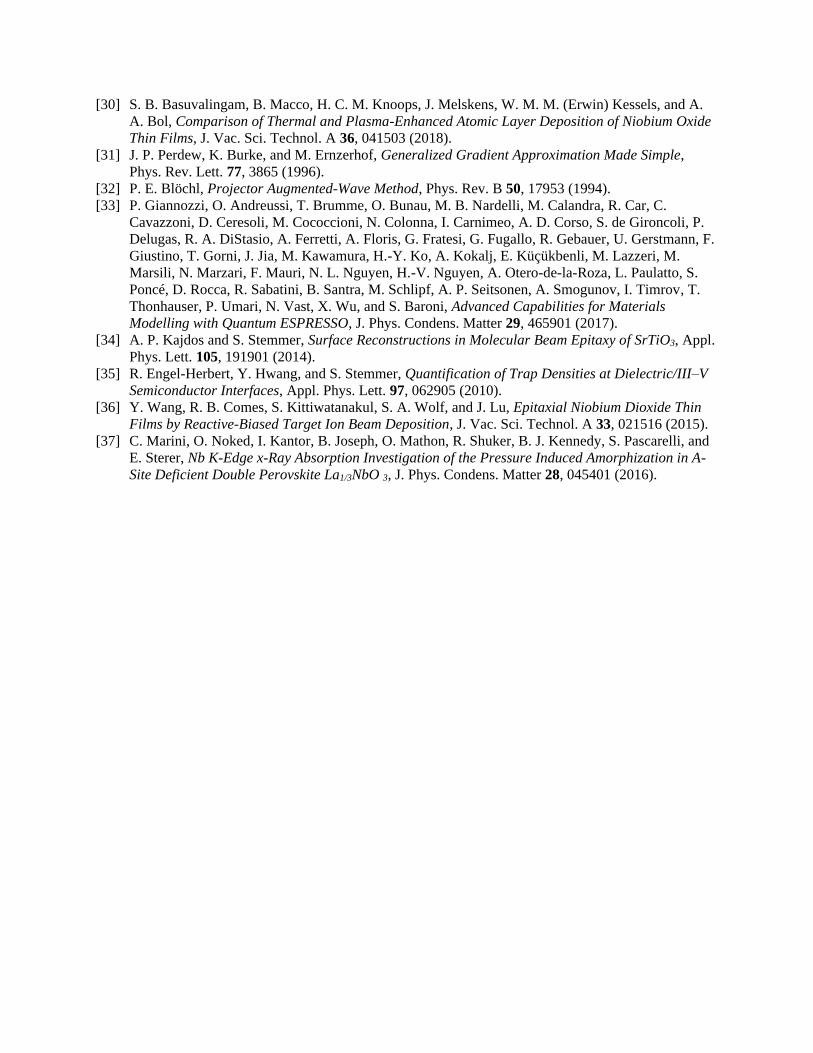
consistently improved RHEED images after capping with SHO, which can be found in supporting materials
in Figure S1. This indicates high crystallinity of the SHO capping layer and better preservation of SNO
from over-oxidation during cooldown. It should be noted that the medium-capped SNO sample shows
relatively weak RHEED pattern after SHO capping as found in Figure S1 because of inconsistent Hf flux
that produced a Hf-rich capping layer.
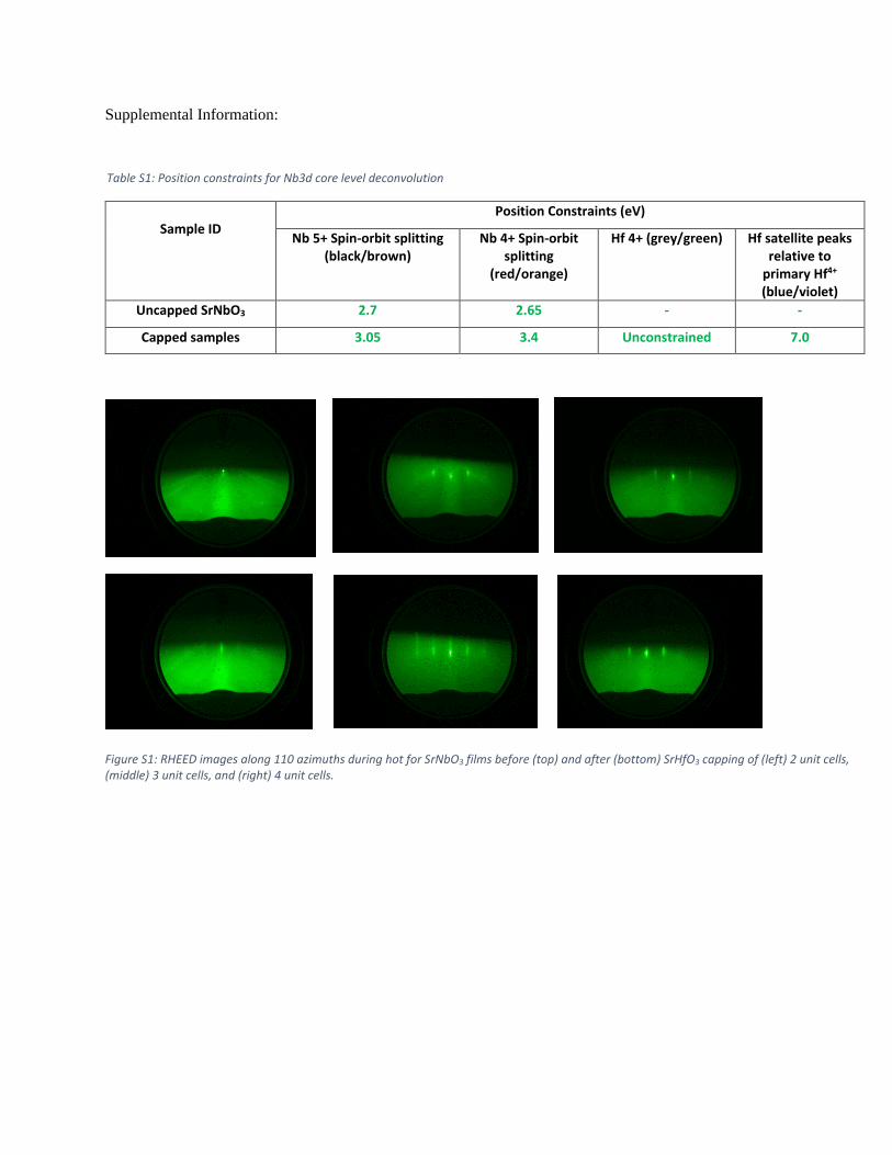
AFM measurements were performed to verify the surface morphology of the SNO films. Figure 3(c) shows
the AFM topography of uncapped SNO film grown on GSO substrate with surface roughness of ~ 1.1 nm
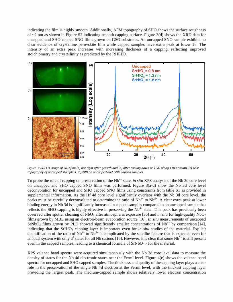
indicating the film is highly smooth. Additionally, AFM topography of SHO shows the surface roughness
of ~2 nm as shown in Figure S2 indicating smooth capping surface. Figure 3(d) shows the XRD data for
uncapped and SHO capped SNO films grown on GSO substrates. An uncapped SNO sample exhibits no
clear evidence of crystalline perovskite film while capped samples have extra peak at lower 2θ. The
intensity of an extra peak increases with increasing thickness of a capping, reflecting improved
stoichiometry and crystallinity as predicted by the RHEED.
Figure 3: RHEED image of SNO film (a) hot right after growth and (b) after cooling down on GSO along 110 azimuth, (c) AFM topography of uncapped SNO films, (d) XRD on uncapped and SHO capped samples
To probe the role of capping on preservation of the Nb4+ state, in situ XPS analysis of the Nb 3d core level
on uncapped and SHO capped SNO films was performed. Figure 3(a-d) show the Nb 3d core level
deconvolution for uncapped and SHO capped SNO films using constraints from table S1 as provided in
supplemental information. As the Hf 4d core level significantly overlaps with the Nb 3d core level, the
peaks must be carefully deconvoluted to determine the ratio of Nb4+ to Nb5+. A clear extra peak at lower
binding energy in Nb 3d is significantly increased in capped samples compared to an uncapped sample that
reflects the SHO capping is highly effective in preserving the Nb4+ state. This peak has previously been
observed after sputter cleaning of NbO2 after atmospheric exposure [36] and in situ for high-quality NbO2
films grown by MBE using an electron-beam evaporation source [16]. In situ measurements of uncapped
SrNbO3 films grown by PLD showed significantly smaller concentrations of Nb4+ by comparison [14],
indicating that the SrHfO3 capping layer is important even for in situ studies of the material. Explicit
quantification of the ratio of Nb4+ to Nb5+ is complicated by the satellite feature that is expected even for
an ideal system with only d1 states for all Nb cations [16]. However, it is clear that some Nb5+ is still present
even in the capped samples, leading to a chemical formula of SrNbO3+δ for the material.
XPS valence band spectra were acquired simultaneously with the Nb 3d core level data to measure the
density of states for the Nb 4d electronic states near the Fermi level. Figure 4(e) shows the valence band
spectra for uncapped and SHO capped samples. The thickness and quality of the capping layer plays a clear
role in the preservation of the single Nb 4d electron at the Fermi level, with the thickest capping layer
providing the largest peak. The medium-capped sample shows relatively lower electron concentration
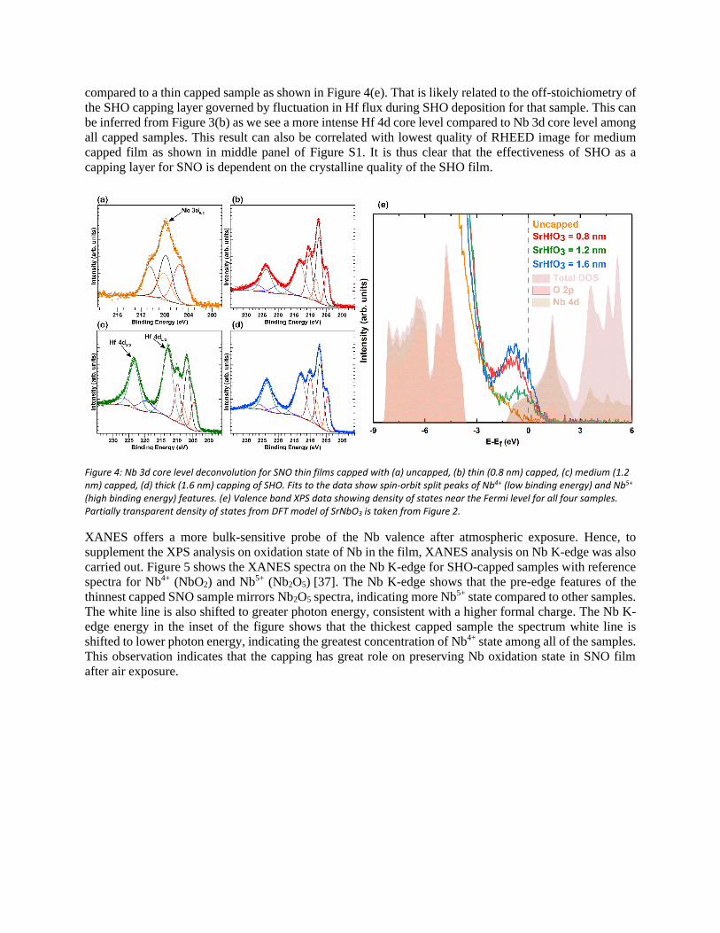
compared to a thin capped sample as shown in Figure 4(e). That is likely related to the off-stoichiometry of
the SHO capping layer governed by fluctuation in Hf flux during SHO deposition for that sample. This can
be inferred from Figure 3(b) as we see a more intense Hf 4d core level compared to Nb 3d core level among
all capped samples. This result can also be correlated with lowest quality of RHEED image for medium
capped film as shown in middle panel of Figure S1. It is thus clear that the effectiveness of SHO as a
capping layer for SNO is dependent on the crystalline quality of the SHO film.
Figure 4: Nb 3d core level deconvolution for SNO thin films capped with (a) uncapped, (b) thin (0.8 nm) capped, (c) medium (1.2 nm) capped, (d) thick (1.6 nm) capping of SHO. Fits to the data show spin-orbit split peaks of Nb4+ (low binding energy) and Nb5+ (high binding energy) features. (e) Valence band XPS data showing density of states near the Fermi level for all four samples. Partially transparent density of states from DFT model of SrNbO3 is taken from Figure 2.
XANES offers a more bulk-sensitive probe of the Nb valence after atmospheric exposure. Hence, to
supplement the XPS analysis on oxidation state of Nb in the film, XANES analysis on Nb K-edge was also
carried out. Figure 5 shows the XANES spectra on the Nb K-edge for SHO-capped samples with reference
spectra for Nb4+ (NbO2) and Nb5+ (Nb2O5) [37]. The Nb K-edge shows that the pre-edge features of the
thinnest capped SNO sample mirrors Nb2O5 spectra, indicating more Nb5+ state compared to other samples.
The white line is also shifted to greater photon energy, consistent with a higher formal charge. The Nb K-
edge energy in the inset of the figure shows that the thickest capped sample the spectrum white line is
shifted to lower photon energy, indicating the greatest concentration of Nb4+ state among all of the samples.
This observation indicates that the capping has great role on preserving Nb oxidation state in SNO film
after air exposure.
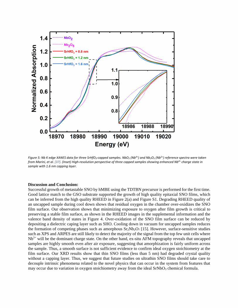
Figure 5: Nb K edge XANES data for three SrHfO3-capped samples. NbO2 (Nb4+) and Nb2O5 (Nb5+) reference spectra were taken from Marini, et al. [37]. (Inset) High-resolution perspective of three capped samples showing enhanced Nb4+ charge state in sample with 1.6 nm capping layer.
Discussion and Conclusion:
Successful growth of metastable SNO by hMBE using the TDTBN precursor is performed for the first time.
Good lattice match to the GSO substrate supported the growth of high quality epitaxial SNO films, which
can be inferred from the high quality RHEED in Figure 2(a) and Figure S1. Degrading RHEED quality of
an uncapped sample during cool down shows that residual oxygen in the chamber over-oxidizes the SNO
film surface. Our observation shows that minimizing exposure to oxygen after film growth is critical to
preserving a stable film surface, as shown in the RHEED images in the supplemental information and the
valence band density of states in Figure 4. Over-oxidation of the SNO film surface can be reduced by
depositing a dielectric caping layer such as SHO. Cooling down in vacuum for uncapped samples reduces
the formation of competing phases such as amorphous Sr2Nb2O7 [15]. However, surface-sensitive studies
such as XPS and ARPES are still likely to detect the majority of the signal from the top few unit cells where
Nb5+ will be the dominant charge state. On the other hand, ex-situ AFM topography reveals that uncapped
samples are highly smooth even after air exposure, suggesting that amorphization is fairly uniform across
the sample. Thus, a smooth surface is not sufficient evidence to confirm ideal oxygen stoichiometry at the
film surface. Our XRD results show that thin SNO films (less than 5 nm) had degraded crystal quality
without a capping layer. Thus, we suggest that future studies on ultrathin SNO films should take care to
decouple intrinsic phenomena related to the novel physics that can occur in the system from features that
may occur due to variation in oxygen stoichiometry away from the ideal SrNbO3 chemical formula.
In conclusion, our study of the synthesis of metastable SrNbO3+δ thin films demonstrates the capabilities of
the hMBE technique with a new TDTBN precursor. As predicted by our DFT calculations, the SNO films
have valence band features at the Fermi level based on XPS analysis which is strongly dependent on the
Nb charge state. The surface of the sample is preserved during cooldown by depositing a capping layer of
SrHfO3 immediately after SrNbO3 growth, which increases the electronic density of states near the Fermi
level. XRD, XAS and XPS used to characterize the SNO film and effectiveness of the SHO capping at
various thicknesses indicate that both the quality and the thickness of the capping layer are important to
preserving the surface. The ability to deposit SrNbO3 films by hMBE opens the door for future exploration
of interfacial phenomena in heterostructures, which has not been explored previously in films.
Acknowledgements:
ST and RBC gratefully acknowledge support from the Air Force Office of Scientific Research under award
number FA9550-20-1-0034. This research used resources of the Advanced Photon Source, an Office of
Science User Facility operated for the U.S. Department of Energy (DOE) Office of Science by Argonne
National Laboratory, and was supported by the U.S. DOE under Contract No. DE-AC02-06CH11357.
References:
[1] A. Ohtomo and H. Y. Hwang, A High-Mobility Electron Gas at the LaAlO 3 /SrTiO 3
Heterointerface, Nature 427, 6973 (2004).
[2] Y. Chen and R. J. Green, Progress and Perspectives of Atomically Engineered Perovskite Oxide
Interfaces for Electronics and Electrocatalysts, Adv. Mater. Interfaces 6, 1900547 (2019).
[3] J. Mannhart, D. H. A. Blank, H. Y. Hwang, A. J. Millis, and J.-M. Triscone, Two-Dimensional
Electron Gases at Oxide Interfaces, MRS Bull. 33, 1027 (2008).
[4] D. Oka, Y. Hirose, S. Nakao, T. Fukumura, and T. Hasegawa, Intrinsic High Electrical
Conductivity of Stoichiometric SrNbO3 Epitaxial Thin Films, Phys. Rev. B 92, 205102 (2015).
[5] Z. Zhong and P. Hansmann, Band Alignment and Charge Transfer in Complex Oxide Interfaces,
Phys. Rev. X 7, 011023 (2017).
[6] Z. Zhong and P. Hansmann, Tuning the Work Function in Transition Metal Oxides and Their
Heterostructures, Phys. Rev. B 93, 235116 (2016).
[7] D. Y. Wan, Y. L. Zhao, Y. Cai, T. C. Asmara, Z. Huang, J. Q. Chen, J. Hong, S. M. Yin, C. T.
Nelson, M. R. Motapothula, B. X. Yan, D. Xiang, X. Chi, H. Zheng, W. Chen, R. Xu, Ariando, A.
Rusydi, A. M. Minor, M. B. H. Breese, M. Sherburne, M. Asta, Q.-H. Xu, and T. Venkatesan,
Electron Transport and Visible Light Absorption in a Plasmonic Photocatalyst Based on Strontium
Niobate, Nat. Commun. 8, 1 (2017).
[8] J. Roth, A. Paul, N. Goldner, A. Pogrebnyakov, K. Agueda, T. Birol, N. Alem, and R. Engel-
Herbert, Sputtered SrxNbO3 as a UV-Transparent Conducting Film, ACS Appl. Mater. Interfaces
12, 30520 (2020).
[9] Y. Park, J. Roth, D. Oka, Y. Hirose, T. Hasegawa, A. Paul, A. Pogrebnyakov, V. Gopalan, T. Birol,
and R. Engel-Herbert, SrNbO3 as a Transparent Conductor in the Visible and Ultraviolet Spectra,
Commun. Phys. 3, 102 (2020).
[10] M. Mirjolet, M. Kataja, T. K. Hakala, P. Komissinskiy, L. Alff, G. Herranz, and J. Fontcuberta,
Optical Plasmon Excitation in Transparent Conducting SrNbO3 and SrVO3 Thin Films, Adv. Opt.
Mater. 9, 2100520 (2021).
[11] J. M. Ok, N. Mohanta, J. Zhang, S. Yoon, S. Okamoto, E. S. Choi, H. Zhou, M. Briggeman, P.
Irvin, A. R. Lupini, Y.-Y. Pai, E. Skoropata, C. Sohn, H. Li, H. Miao, B. Lawrie, W. S. Choi, G.
Eres, J. Levy, and H. N. Lee, Correlated Oxide Dirac Semimetal in the Extreme Quantum Limit,
Sci. Adv. 7, eabf9631 (2021).
[12] J. Zhang, J. M. Ok, Y.-Y. Pai, J. Lapano, E. Skoropata, A. R. Mazza, H. Li, A. Huon, S. Yoon, B.
Lawrie, M. Brahlek, T. Z. Ward, G. Eres, H. Miao, and H. N. Lee, Extremely Large
Magnetoresistance in High-Mobility SrNbO3/SrTiO3 Heterostructures, Phys. Rev. B 104, L161404
(2021).
[13] D. Oka, Y. Hirose, S. Nakao, T. Fukumura, and T. Hasegawa, Intrinsic High Electrical
Conductivity of Stoichiometric SrNbO3 Epitaxial Thin Films, Phys. Rev. B 92, 205102 (2015).
[14] C. Bigi, P. Orgiani, J. Sławińska, J. Fujii, J. T. Irvine, S. Picozzi, G. Panaccione, I. Vobornik, G.
Rossi, D. Payne, and F. Borgatti, Direct Insight into the Band Structure of SrNbO3, Phys. Rev.
Mater. 4, 025006 (2020).
[15] K. R. Balasubramaniam, Y. Cao, N. Patel, S. Havelia, P. J. Cox, E. C. Devlin, E. P. Yu, B. J. Close,
P. M. Woodward, and P. A. Salvador, Phase and Structural Characterization of Sr2Nb2O7 and
SrNbO3 Thin Films Grown via Pulsed Laser Ablation in O2 or N2 Atmospheres, J. Solid State
Chem. 181, 705 (2008).
[16] C. Lin, A. Posadas, T. Hadamek, and A. A. Demkov, Final-State Effect on x-Ray Photoelectron
Spectrum of Nominally d1 and n-Doped d0 Transition-Metal Oxides, Phys. Rev. B 92, 035110
(2015).
[17] Z. H. Lim, N. F. Quackenbush, A. N. Penn, M. Chrysler, M. Bowden, Z. Zhu, J. M. Ablett, T.-L.
Lee, J. M. LeBeau, J. C. Woicik, P. V. Sushko, S. A. Chambers, and J. H. Ngai, Charge Transfer
and Built-in Electric Fields between a Crystalline Oxide and Silicon, Phys. Rev. Lett. 123, 026805
(2019).
[18] C. Chen, Z. Wang, F. Lichtenberg, Y. Ikuhara, and J. G. Bednorz, Patterning Oxide Nanopillars at
the Atomic Scale by Phase Transformation, Nano Lett. 15, 6469 (2015).
[19] C. Chen, S. Lv, Z. Wang, K. Akagi, F. Lichtenberg, Y. Ikuhara, and J. G. Bednorz, Atomic and
Electronic Structure of the SrNbO3/SrNbO3.4 Interface, Appl. Phys. Lett. 105, 221602 (2014).
[20] P. Xu, Y. Ayino, C. Cheng, V. S. Pribiag, R. B. Comes, P. V. Sushko, S. A. Chambers, and B.
Jalan, Predictive Control over Charge Density in the Two-Dimensional Electron Gas at the Polar-
Nonpolar NdTiO3/SrTiO3 Interface, Phys. Rev. Lett. 117, 106803 (2016).
[21] R. Aeschlimann, D. Preziosi, P. Scheiderer, M. Sing, S. Valencia, J. Santamaria, C. Luo, H. Ryll, F.
Radu, R. Claessen, C. Piamonteze, and M. Bibes, A Living-Dead Magnetic Layer at the Surface of
Ferrimagnetic DyTiO3 Thin Films, Adv. Mater. 30, 1707489 (2018).
[22] C. Rossel, M. Sousa, C. Marchiori, J. Fompeyrine, D. Webb, D. Caimi, B. Mereu, A. Ispas, J. P.
Locquet, H. Siegwart, R. Germann, A. Tapponnier, and K. Babich, SrHfO3 as Gate Dielectric for
Future CMOS Technology, Microelectron. Eng. 84, 1869 (2007).
[23] M. Brahlek, A. S. Gupta, J. Lapano, J. Roth, H.-T. Zhang, L. Zhang, R. Haislmaier, and R. Engel-
Herbert, Frontiers in the Growth of Complex Oxide Thin Films: Past, Present, and Future of Hybrid
MBE, Adv. Funct. Mater. 28, 1702772 (2018).
[24] C. Eaton, J. A. Moyer, H. M. Alipour, E. D. Grimley, M. Brahlek, J. M. LeBeau, and R. Engel-
Herbert, Growth of SrVO3 Thin Films by Hybrid Molecular Beam Epitaxy, J. Vac. Sci. Technol. A
33, 061504 (2015).
[25] A. Prakash, T. Wang, R. Choudhary, G. Haugstad, W. L. Gladfelter, and B. Jalan, Precursor
Selection in Hybrid Molecular Beam Epitaxy of Alkaline-Earth Stannates, J. Vac. Sci. Technol. A
38, 063410 (2020).
[26] B. Jalan, R. Engel-Herbert, N. J. Wright, and S. Stemmer, Growth of High-Quality SrTiO3 Films
Using a Hybrid Molecular Beam Epitaxy Approach, J. Vac. Sci. Technol. A 27, 461 (2009).
[27] S. Thapa, S. R. Provence, W. Jin, J. Lapano, J. T. Sadowski, M. Brahlek, and R. B. Comes,
Correlating Surface Stoichiometry and Termination in SrTiO3 Films Grown by Hybrid Molecular
Beam Epitaxy, Jour. Vac. Sci. & Tech. A 39, 053203 (2021)
[28] K. Kukli, M. Ritala, M. Leskelä, and R. Lappalainen, Niobium Oxide Thin Films Grown by Atomic
Layer Epitaxy, Chem. Vap. Depos. 4, 29 (1998).
[29] T. Blanquart, J. Niinistö, M. Heikkilä, T. Sajavaara, K. Kukli, E. Puukilainen, C. Xu, W. Hunks, M.
Ritala, and M. Leskelä, Evaluation and Comparison of Novel Precursors for Atomic Layer
Deposition of Nb2O5 Thin Films, Chem. Mater. 24, 975 (2012).
[30] S. B. Basuvalingam, B. Macco, H. C. M. Knoops, J. Melskens, W. M. M. (Erwin) Kessels, and A.
A. Bol, Comparison of Thermal and Plasma-Enhanced Atomic Layer Deposition of Niobium Oxide
Thin Films, J. Vac. Sci. Technol. A 36, 041503 (2018).
[31] J. P. Perdew, K. Burke, and M. Ernzerhof, Generalized Gradient Approximation Made Simple,
Phys. Rev. Lett. 77, 3865 (1996).
[32] P. E. Blöchl, Projector Augmented-Wave Method, Phys. Rev. B 50, 17953 (1994).
[33] P. Giannozzi, O. Andreussi, T. Brumme, O. Bunau, M. B. Nardelli, M. Calandra, R. Car, C.
Cavazzoni, D. Ceresoli, M. Cococcioni, N. Colonna, I. Carnimeo, A. D. Corso, S. de Gironcoli, P.
Delugas, R. A. DiStasio, A. Ferretti, A. Floris, G. Fratesi, G. Fugallo, R. Gebauer, U. Gerstmann, F.
Giustino, T. Gorni, J. Jia, M. Kawamura, H.-Y. Ko, A. Kokalj, E. Küçükbenli, M. Lazzeri, M.
Marsili, N. Marzari, F. Mauri, N. L. Nguyen, H.-V. Nguyen, A. Otero-de-la-Roza, L. Paulatto, S.
Poncé, D. Rocca, R. Sabatini, B. Santra, M. Schlipf, A. P. Seitsonen, A. Smogunov, I. Timrov, T.
Thonhauser, P. Umari, N. Vast, X. Wu, and S. Baroni, Advanced Capabilities for Materials
Modelling with Quantum ESPRESSO, J. Phys. Condens. Matter 29, 465901 (2017).
[34] A. P. Kajdos and S. Stemmer, Surface Reconstructions in Molecular Beam Epitaxy of SrTiO3, Appl.
Phys. Lett. 105, 191901 (2014).
[35] R. Engel-Herbert, Y. Hwang, and S. Stemmer, Quantification of Trap Densities at Dielectric/III–V
Semiconductor Interfaces, Appl. Phys. Lett. 97, 062905 (2010).
[36] Y. Wang, R. B. Comes, S. Kittiwatanakul, S. A. Wolf, and J. Lu, Epitaxial Niobium Dioxide Thin
Films by Reactive-Biased Target Ion Beam Deposition, J. Vac. Sci. Technol. A 33, 021516 (2015).
[37] C. Marini, O. Noked, I. Kantor, B. Joseph, O. Mathon, R. Shuker, B. J. Kennedy, S. Pascarelli, and
E. Sterer, Nb K-Edge x-Ray Absorption Investigation of the Pressure Induced Amorphization in A-
Site Deficient Double Perovskite La1/3NbO 3, J. Phys. Condens. Matter 28, 045401 (2016).
Supplemental Information:
Sample ID
Position Constraints (eV)
Nb 5+ Spin-orbit splitting (black/brown)
Nb 4+ Spin-orbit splitting
(red/orange)
Hf 4+ (grey/green) Hf satellite peaks relative to
primary Hf4+ (blue/violet)
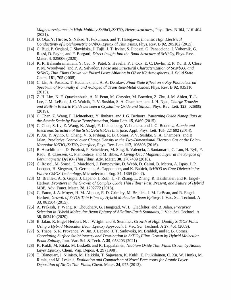
Uncapped SrNbO3 2.7 2.65 - -
Capped samples 3.05 3.4 Unconstrained 7.0
Table S1: Position constraints for Nb3d core level deconvolution
Figure S1: RHEED images along 110 azimuths during hot for SrNbO3 films before (top) and after (bottom) SrHfO3 capping of (left) 2 unit cells, (middle) 3 unit cells, and (right) 4 unit cells.
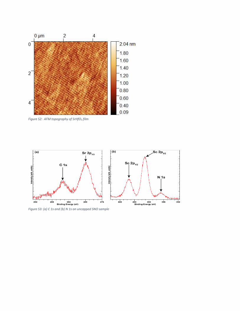
Figure S3: (a) C 1s and (b) N 1s on uncapped SNO sample
Figure S2: AFM topography of SrHfO3 film
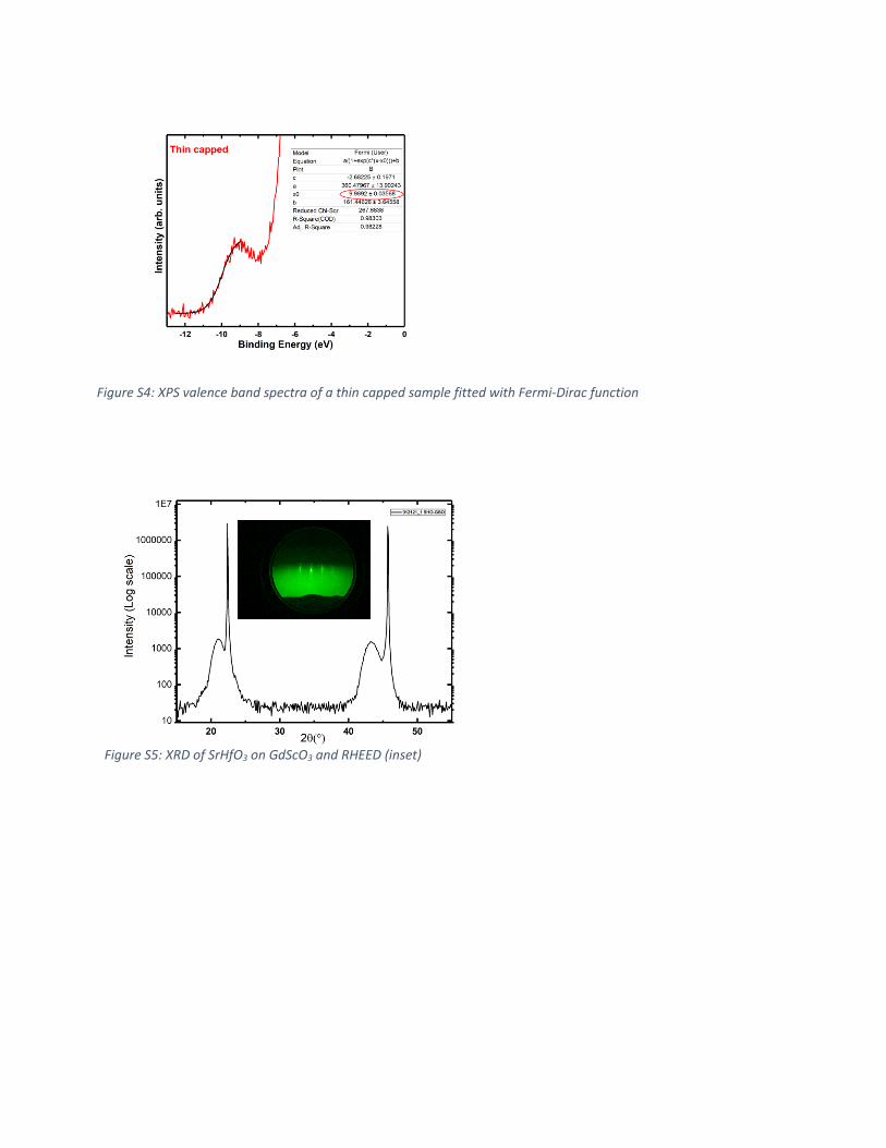
Figure S5: XRD of SrHfO3 on GdScO3 and RHEED (inset)
Figure S4: XPS valence band spectra of a thin capped sample fitted with Fermi-Dirac function