
SUBJECT-BASIC ELECTRONICS ENGINEERING TOPIC PROBLEM …
29
SUBJECT-BASIC ELECTRONICS ENGINEERING TOPIC-PROBLEM AND SOLUTIONS Prepared by Mr. Bikash Meher Assistant Professor Department-EE Topic includes Diode BJT and Biasing FET and MOSFET OP-AMP
Transcript of SUBJECT-BASIC ELECTRONICS ENGINEERING TOPIC PROBLEM …
SUBJECT-BASIC ELECTRONICS ENGINEERING
TOPIC-PROBLEM AND SOLUTIONS
Prepared by Mr. Bikash Meher
Assistant Professor
Department-EE
Topic includes
Diode
BJT and Biasing
FET and MOSFET
OP-AMP
2
Semicondutor Diode
Semiconductor Diode
Problems and Solutions
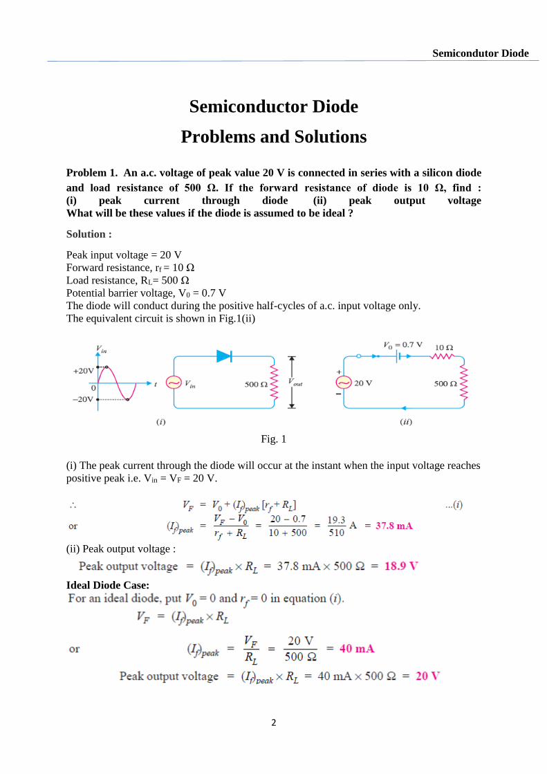
Problem 1. An a.c. voltage of peak value 20 V is connected in series with a silicon diode
and load resistance of 500 Ω. If the forward resistance of diode is 10 Ω, find :
(i) peak current through diode (ii) peak output voltage
What will be these values if the diode is assumed to be ideal ?
Solution :
Peak input voltage = 20 V
Forward resistance, rf = 10 Ω
Load resistance, RL= 500 Ω
Potential barrier voltage, V0 = 0.7 V
The diode will conduct during the positive half-cycles of a.c. input voltage only.
The equivalent circuit is shown in Fig.1(ii)
Fig. 1
(i) The peak current through the diode will occur at the instant when the input voltage reaches
positive peak i.e. Vin = VF = 20 V.
(ii) Peak output voltage :
Ideal Diode Case:
3
Semicondutor Diode
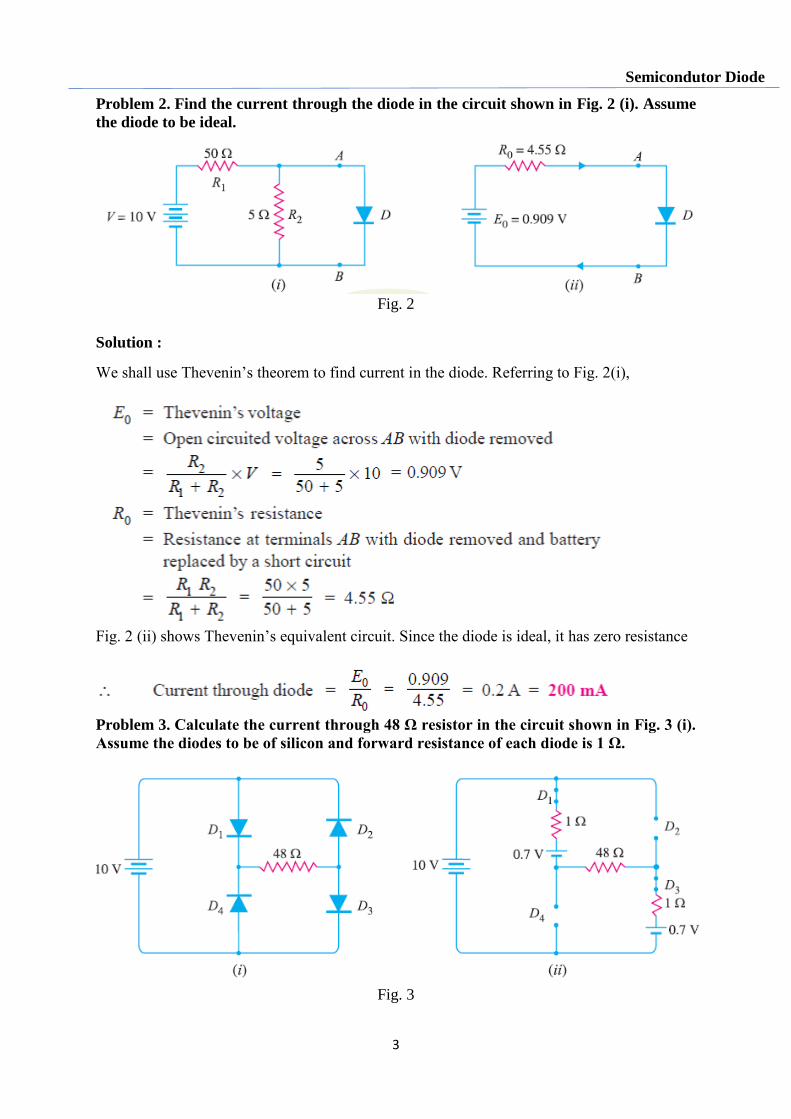
Problem 2. Find the current through the diode in the circuit shown in Fig. 2 (i). Assume
the diode to be ideal.
Fig. 2
Solution :
We shall use Thevenin’s theorem to find current in the diode. Referring to Fig. 2(i),
Fig. 2 (ii) shows Thevenin’s equivalent circuit. Since the diode is ideal, it has zero resistance
Problem 3. Calculate the current through 48 Ω resistor in the circuit shown in Fig. 3 (i).
Assume the diodes to be of silicon and forward resistance of each diode is 1 Ω.
Fig. 3
4
Semicondutor Diode
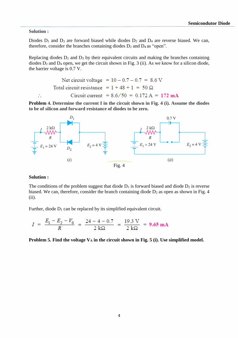
Solution :
Diodes D1 and D3 are forward biased while diodes D2 and D4 are reverse biased. We can,
therefore, consider the branches containing diodes D2 and D4 as “open”.
Replacing diodes D1 and D3 by their equivalent circuits and making the branches containing
diodes D2 and D4 open, we get the circuit shown in Fig. 3 (ii). As we know for a silicon diode,
the barrier voltage is 0.7 V.
Problem 4. Determine the current I in the circuit shown in Fig. 4 (i). Assume the diodes
to be of silicon and forward resistance of diodes to be zero.
Fig. 4
Solution :
The conditions of the problem suggest that diode D1 is forward biased and diode D2 is reverse
biased. We can, therefore, consider the branch containing diode D2 as open as shown in Fig. 4
(ii).
Further, diode D1 can be replaced by its simplified equivalent circuit.
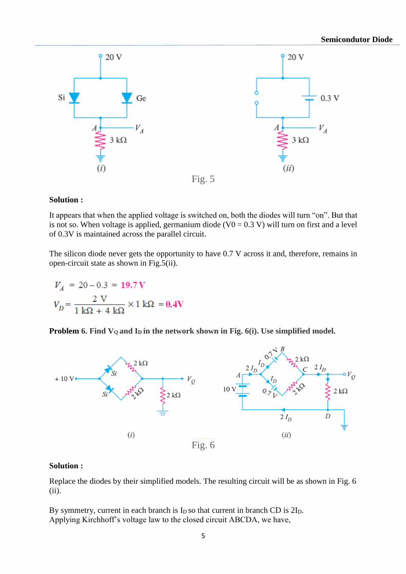
Problem 5. Find the voltage VA in the circuit shown in Fig. 5 (i). Use simplified model.
5
Semicondutor Diode
Fig. 5
Solution :
It appears that when the applied voltage is switched on, both the diodes will turn “on”. But that
is not so. When voltage is applied, germanium diode (V0 = 0.3 V) will turn on first and a level
of 0.3V is maintained across the parallel circuit.
The silicon diode never gets the opportunity to have 0.7 V across it and, therefore, remains in
open-circuit state as shown in Fig.5(ii).
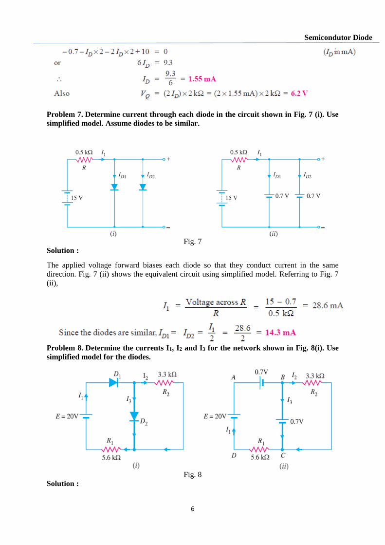
Problem 6. Find VQ and ID in the network shown in Fig. 6(i). Use simplified model.
Fig. 6
Solution :
Replace the diodes by their simplified models. The resulting circuit will be as shown in Fig. 6
(ii).
By symmetry, current in each branch is ID so that current in branch CD is 2ID.
Applying Kirchhoff’s voltage law to the closed circuit ABCDA, we have,
6
Semicondutor Diode
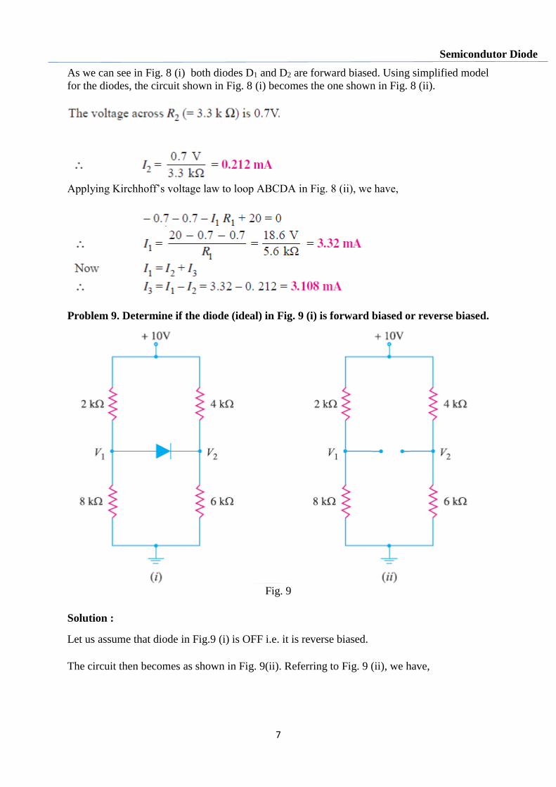
Problem 7. Determine current through each diode in the circuit shown in Fig. 7 (i). Use
simplified model. Assume diodes to be similar.
Fig. 7
Solution :
The applied voltage forward biases each diode so that they conduct current in the same
direction. Fig. 7 (ii) shows the equivalent circuit using simplified model. Referring to Fig. 7
(ii),
Problem 8. Determine the currents I1, I2 and I3 for the network shown in Fig. 8(i). Use
simplified model for the diodes.
Fig. 8
Solution :
7
Semicondutor Diode
As we can see in Fig. 8 (i) both diodes D1 and D2 are forward biased. Using simplified model
for the diodes, the circuit shown in Fig. 8 (i) becomes the one shown in Fig. 8 (ii).
Applying Kirchhoff’s voltage law to loop ABCDA in Fig. 8 (ii), we have,
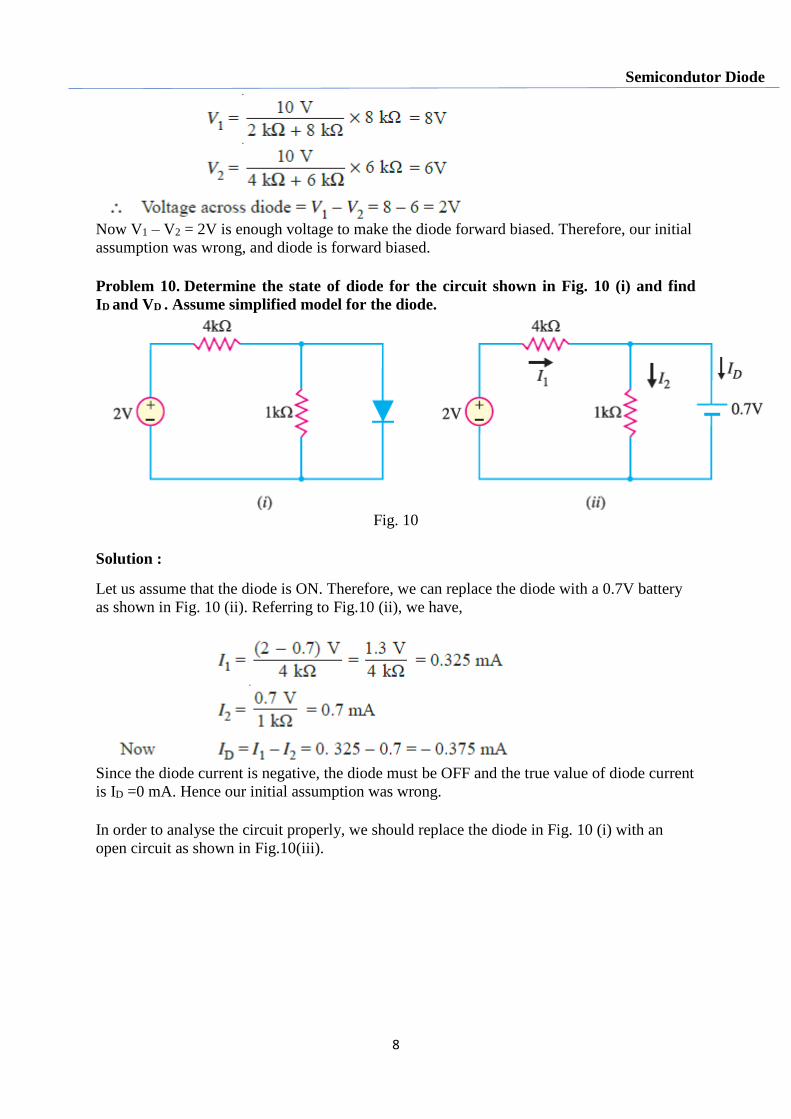
Problem 9. Determine if the diode (ideal) in Fig. 9 (i) is forward biased or reverse biased.
Fig. 9
Solution :
Let us assume that diode in Fig.9 (i) is OFF i.e. it is reverse biased.
The circuit then becomes as shown in Fig. 9(ii). Referring to Fig. 9 (ii), we have,
8
Semicondutor Diode
Now V1 – V2 = 2V is enough voltage to make the diode forward biased. Therefore, our initial
assumption was wrong, and diode is forward biased.
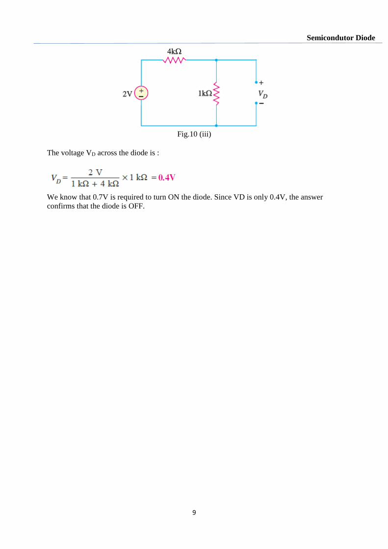
Problem 10. Determine the state of diode for the circuit shown in Fig. 10 (i) and find
ID and VD . Assume simplified model for the diode.
Fig. 10
Solution :
Let us assume that the diode is ON. Therefore, we can replace the diode with a 0.7V battery
as shown in Fig. 10 (ii). Referring to Fig.10 (ii), we have,
Since the diode current is negative, the diode must be OFF and the true value of diode current
is ID =0 mA. Hence our initial assumption was wrong.
In order to analyse the circuit properly, we should replace the diode in Fig. 10 (i) with an
open circuit as shown in Fig.10(iii).
9
Semicondutor Diode
Fig.10 (iii)
The voltage VD across the diode is :
We know that 0.7V is required to turn ON the diode. Since VD is only 0.4V, the answer
confirms that the diode is OFF.
10
Bipolar Junction Transistor
Bipolar Junction Transistor
Problems and Solutions
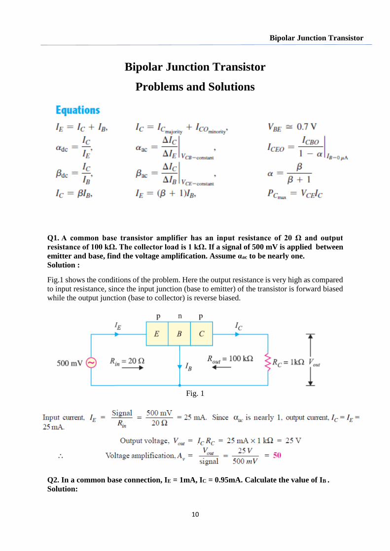
Q1. A common base transistor amplifier has an input resistance of 20 Ω and output
resistance of 100 kΩ. The collector load is 1 kΩ. If a signal of 500 mV is applied between
emitter and base, find the voltage amplification. Assume αac to be nearly one.
Solution :
Fig.1 shows the conditions of the problem. Here the output resistance is very high as compared
to input resistance, since the input junction (base to emitter) of the transistor is forward biased
while the output junction (base to collector) is reverse biased.
Fig. 1
Q2. In a common base connection, IE = 1mA, IC = 0.95mA. Calculate the value of IB .
Solution:
11
Bipolar Junction Transistor
Q3. Find the value of β if (i) α = 0.9 (ii) α = 0.98 (iii) α = 0.99.
Solution :
(i) α = 0.9
(ii) α = 0.98
(iii) α = 0.99
Q4. Calculate IE in a transistor for which β = 50 and IB = 20 μA.
Solution :
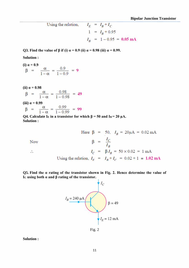
Q5. Find the α rating of the transistor shown in Fig. 2. Hence determine the value of
IC using both α and β rating of the transistor.
Fig. 2
Solution :
12
Bipolar Junction Transistor
Q6. The collector leakage current in a transistor is 300 μA in CE arrangement. If now
the transistor is connected in CB arrangement, what will be the leakage current? Given
that β = 120.
Solution :
Q7. For a certain transistor, IB = 20 μA; IC = 2 mA and β = 80. Calculate ICBO.
Solution :
Q8. Using diagrams, explain the correctness of the relation ICEO = (β + 1)ICBO.
Solution :
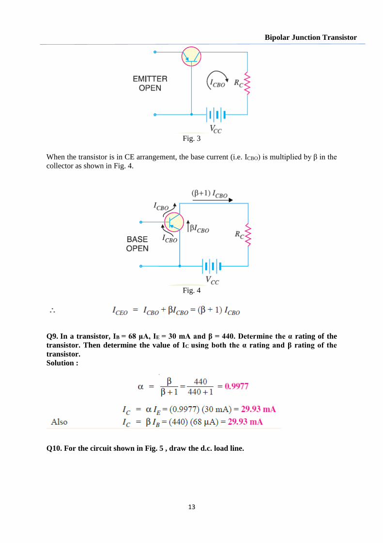
The leakage current ICBO is the current that flows through the base-collector junction when
emitter is open as shown is Fig. 3.
13
Bipolar Junction Transistor
Fig. 3
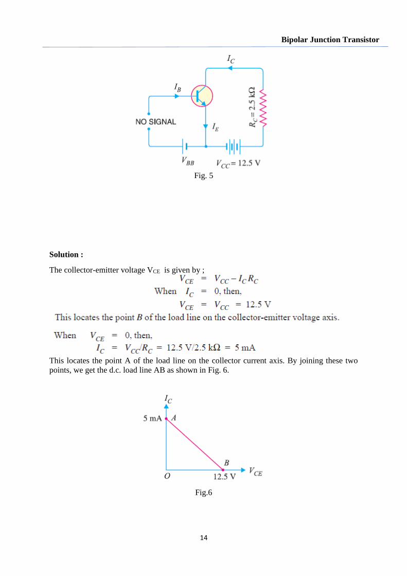
When the transistor is in CE arrangement, the base current (i.e. ICBO) is multiplied by β in the
collector as shown in Fig. 4.
Fig. 4
Q9. In a transistor, IB = 68 μA, IE = 30 mA and β = 440. Determine the α rating of the
transistor. Then determine the value of IC using both the α rating and β rating of the
transistor.
Solution :
Q10. For the circuit shown in Fig. 5 , draw the d.c. load line.
14
Bipolar Junction Transistor
Fig. 5
Solution :
The collector-emitter voltage VCE is given by ;
This locates the point A of the load line on the collector current axis. By joining these two
points, we get the d.c. load line AB as shown in Fig. 6.
Fig.6

15
Bipolar Junction Transistor
16
BJT BIASING
BJT Biasing
Problems and Solutions
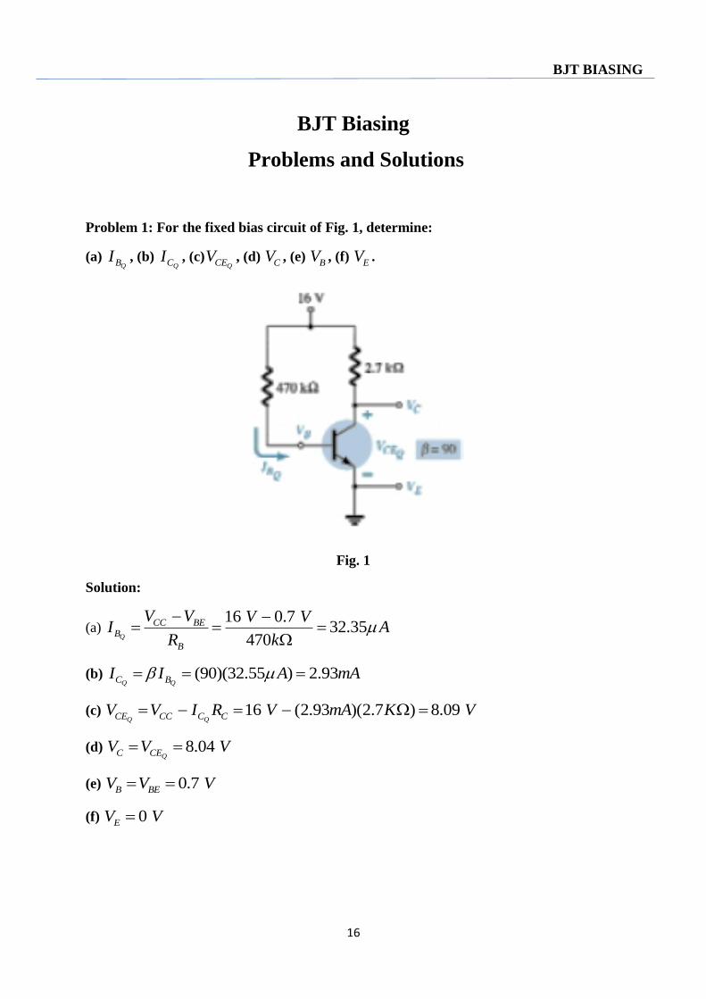
Problem 1: For the fixed bias circuit of Fig. 1, determine:
(a) QBI , (b)
QCI , (c)QCEV , (d)
CV , (e) BV , (f)
EV .
Fig. 1
Solution:
(a) 16 0.7
32.35470Q
CC BEB
B
V V V VI A
R k
(b) (90)(32.55 ) 2.93Q QC BI I A mA
(c) 16 (2.93 )(2.7 ) 8.09Q QCE CC C CV V I R V mA K V
(d) 8.04QC CEV V V
(e) 0.7B BEV V V
(f) 0EV V
17
BJT BIASING
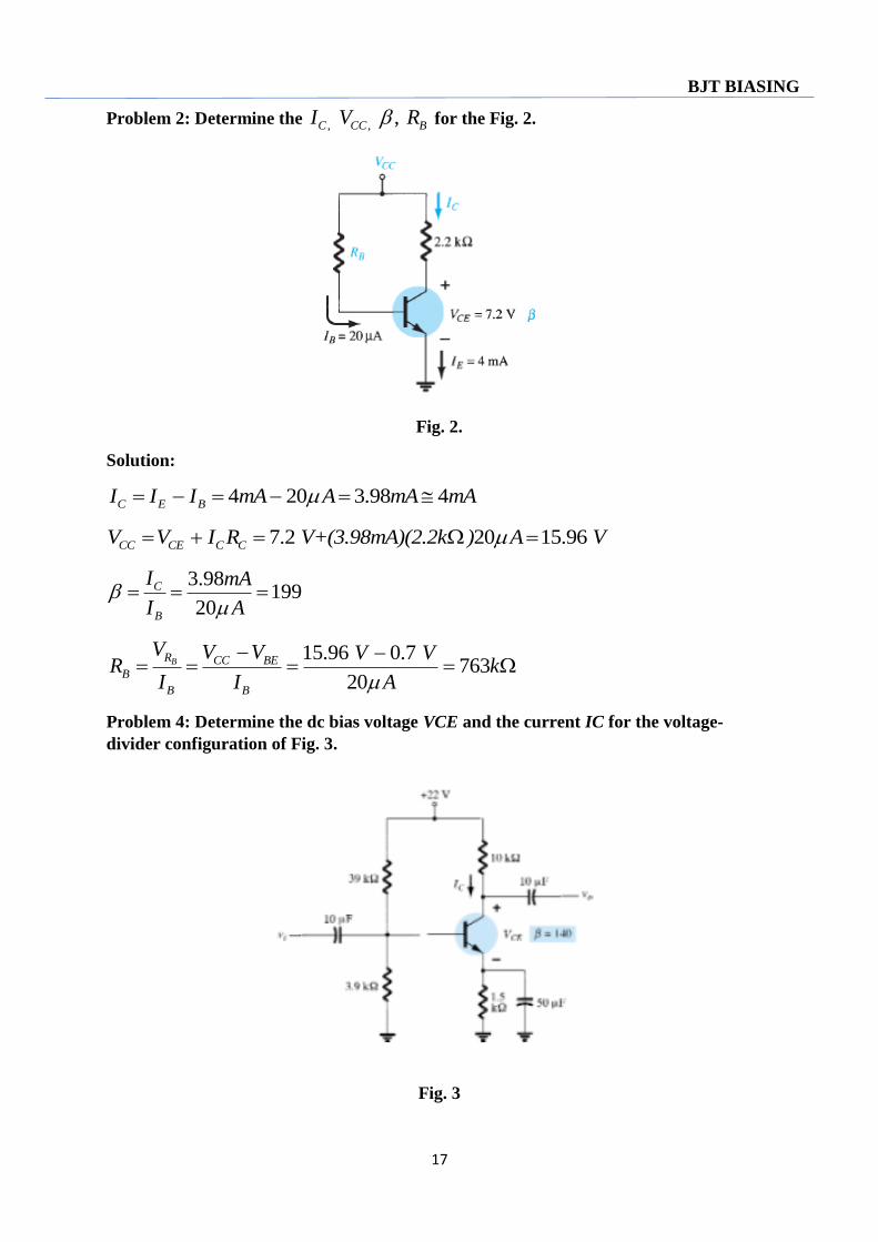
Problem 2: Determine the , , ,C CC BI V R for the Fig. 2.
Fig. 2.
Solution:
4 20 3.98 4C E BI I I mA A mA mA
7.2 20 15.96CC CE C CV V I R V+(3.98mA)(2.2k ) A V
3.98199
20
C
B
I mA
I A
15.96 0.7763
20
BR CC BEB
B B
V V V V VR k
I I A
Problem 4: Determine the dc bias voltage VCE and the current IC for the voltage-
divider configuration of Fig. 3.
Fig. 3
18
BJT BIASING
Solution:
19
BJT BIASING
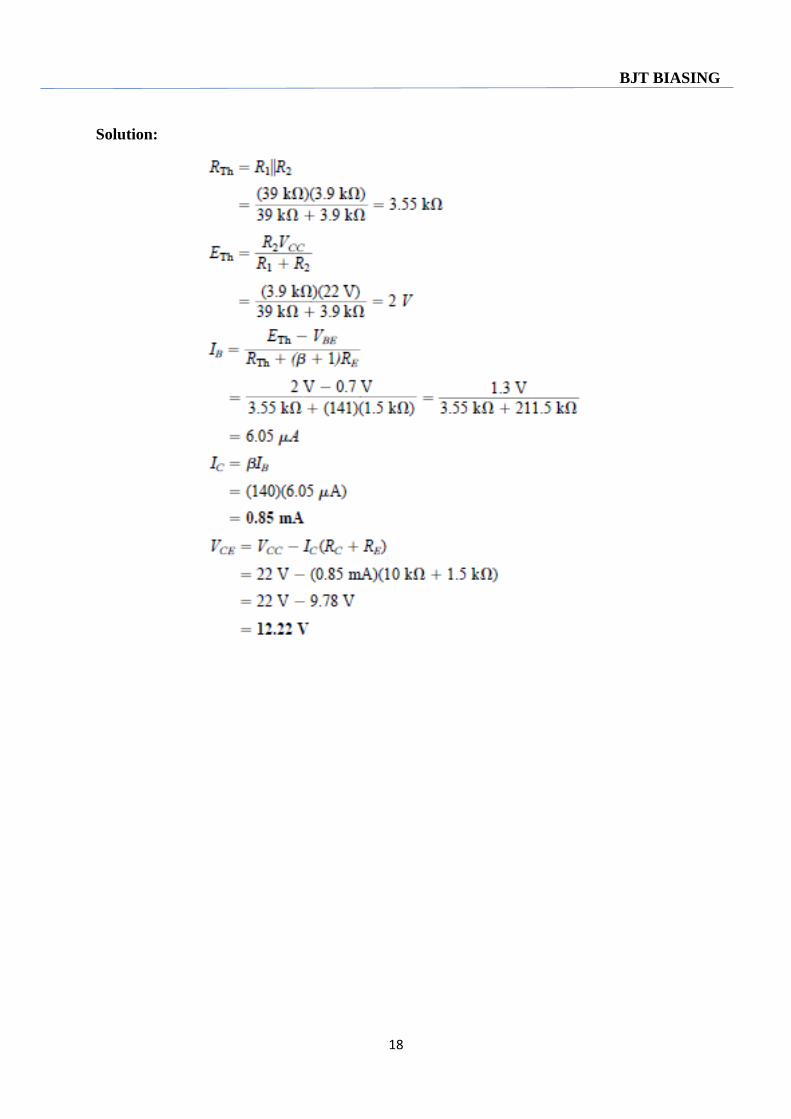
Problem 4: Determine the following voltage divider bias configuration of Fig. 4, using
approximate approach if the condition satisfied for the condition of approximate analysis.
(a) CI , (b)
CEV , (c) BI ,(d)
EV , (e) .BV
Fig. 4
Solution:
(a) 1 2|| || 6.78THR R R =39k 39k k
1 2
(18 )3.13C CC
TH
R V 8.2k VE = V
R +R 39k +8.2k
0.7 )19.02TH BE
TH
TH E
E V 3.13 V VE = A
R +( +1)R 6.78k +(121)(1k )
2.28C BI I mA
(b) ( ) 18 (2.28 )(3.3 1 ) 8.2CE CC C C EV V I R R V mA k k V
(c) 19.02CB
II A
(d) (2.28 )(1 ) 2.28E E E E EV I R I R mA k V
(e) 0.7 2.28 2.98B BE EV V V V V V
20
BJT BIASING
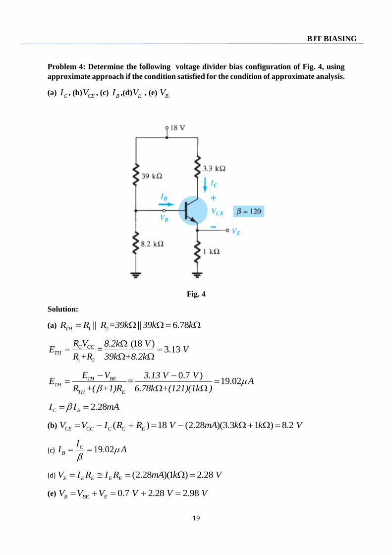
Problem 5: For the voltage divider bias configuration of Fig. 5, determine:
(a) CI , (b)
EV , (c) BV ,(d)
1R
Determine the saturation (satCI ) for the network of Fig. 5.
Fig. 5
Solution:
(a) 18 12
1.284.7
CC CC
C
V V V VI mA
R k
(b) (1.28 )(1.2 ) 1.54E E E C EV I R I R mA k V
(c) 0.7 2.24B BE EV V V V+1.54 V V
(d) 1
1
1
1 , 15.76R
R CC B
R
VR V V V V
I
1 2
2
0.4BR R
VI I mA
R
1
1
1
15.7639.4
0.4
R
R
V VR k
I mA
163.49
3.9 0.68sat
CCC
C E
V VI mA
R R k k
1
FET and MOSFET
FET and MOSFET
Problems and Solutions
Problem 1. Given 9 3.5 ,DSS PI mA and V V determine DI when:
(a) 0 ,GSV V (b) 2 ,GSV V (c) 3.5 ,GSV V (d) 5 .GSV V
Solution:
ID is expressed as
2
1 GSD DSS
P
VI I
V
(a) 0 ,GSV V
2 20
1 9 1 94
GSD DSS
P
V VI I mA mA
V V
(b) 2 ,GSV V
2 22
1 9 1 1.6533.5
GSD DSS
P
V VI I mA mA
V V
(c) 3.5 ,GSV V
2
1 9 1 0GSD DSS
P
V 3.5 VI I mA mA
V 3.5 V
(d) , 0GS P DV V I mA
Problem 2. Given 6DSSI mA and 4PV V :
(a) Determine ID at VGS= –2 V and –3.6 V.
(b) Determine VGS at ID = 3 mA and 5.5 mA.
Solution:
2
FET and MOSFET
(a)
2 22
1 6 1 1.8524.5
GSD DSS
P
V VI I mA mA
V V
2 23.6
1 6 1 0.244.5
GSD DSS
P
V VI I mA mA
V V
(b) 1 DGS P
DSS
IV V
I
3
1 4.5 1 1.13816
DGS P
DSS
I mAV V V V
I mA
5.5
1 4.5 1 0.1926
DGS P
DSS
I mAV V V V
I mA
Problem 3. Given ID=14mA and VGS=1 V, determine VP if IDSS=9.5mA for a depletion –
type MOSFET.
Solution:
1 14.67
0.213951411
9.5
GSP
D
DSS
V VV V
I mA
mAI
4. Given k =0.4×10⁻³A/V2and ID(on) = 3 mA with VGS(on) = 4 V, determine VT.
Solution:
For the enhancement-type MOSFET
2
( )( )D GS on TI k V V
Now VT is expressed as
2
( )( ) DGS on T
IV V
k
( )( ) DGS on T
IV V
k
3
FET and MOSFET
( )D
T GS on
IV V
k
( ) 3
34
0.4 10
4 7.5
1.261
DT GS on
I mAV V V
k
V V
V
1
GCEK, Bhawanipatna
OP-AMP
Operational Amplifier
Problems and Solutions
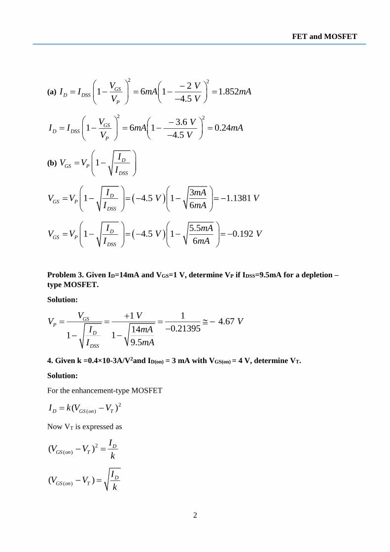
Problem 1: What is the output voltage in the circuit of Fig. 1?
Fig. 1
Solution:
0 1
1
2501.5 18.75
20
fR kV V V V
R k
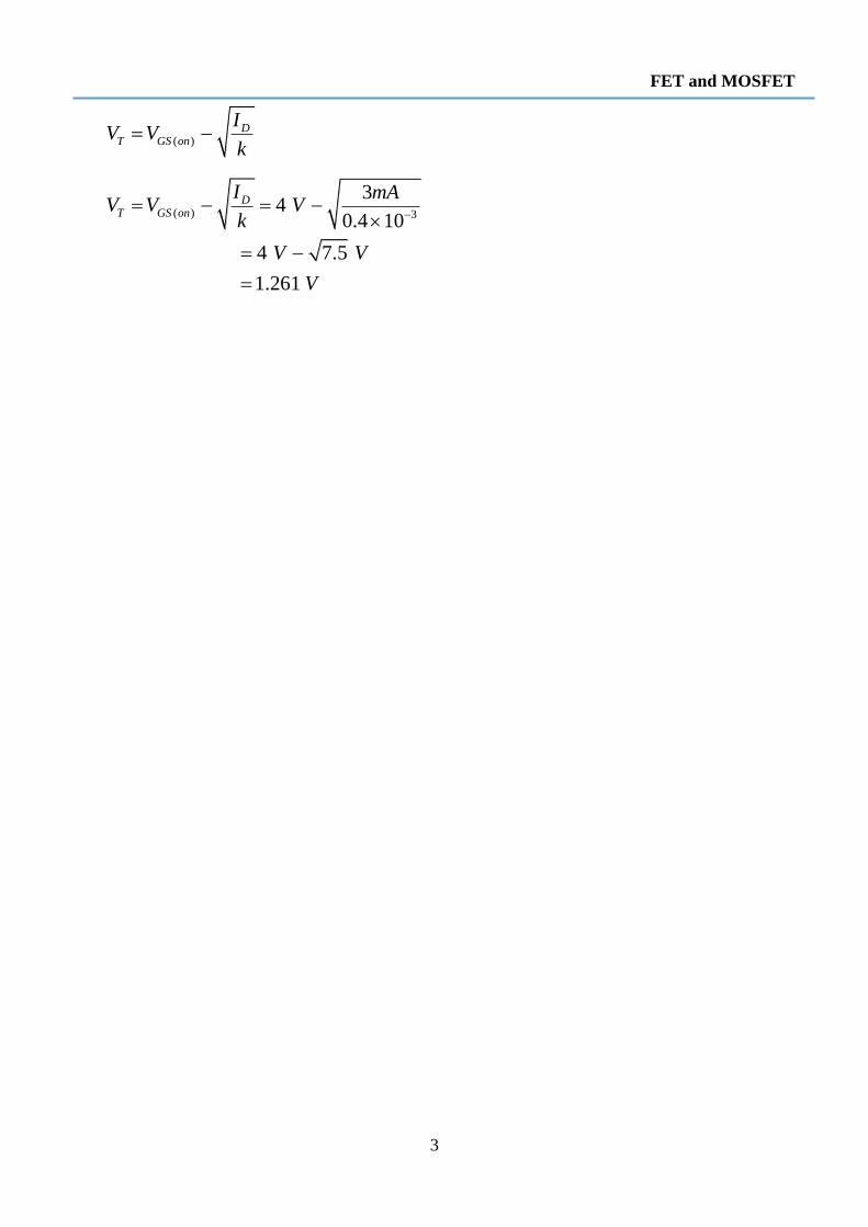
Problem 2: What output voltage results in the circuit of Fig. 2 for an input of V1 = –0.3
V?
Fig. 2
Solution:
0 1
1
3601 1 0.3 9.3
12
fR kV V V V
R k
2
GCEK, Bhawanipatna
OP-AMP
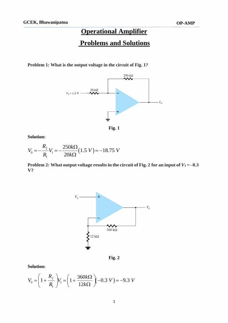
Problem 3: What range of output voltage is developed in the circuit of Fig.3?
Fig. 3
Solution: The output voltage (V0) equation for the Fig. 3 is
0 1
1
1fR
V VR
For R1=10 KΩ,
0 1
1
2001 1 0.5 10.5
10
FR kV V V V
R k
For R1=20 KΩ,
0 1
1
2001 1 0.5 5.5
20
FR kV V V V
R k
So, the output voltage (V0) varies from 5.5 V to 10.5 V.
3
GCEK, Bhawanipatna
OP-AMP
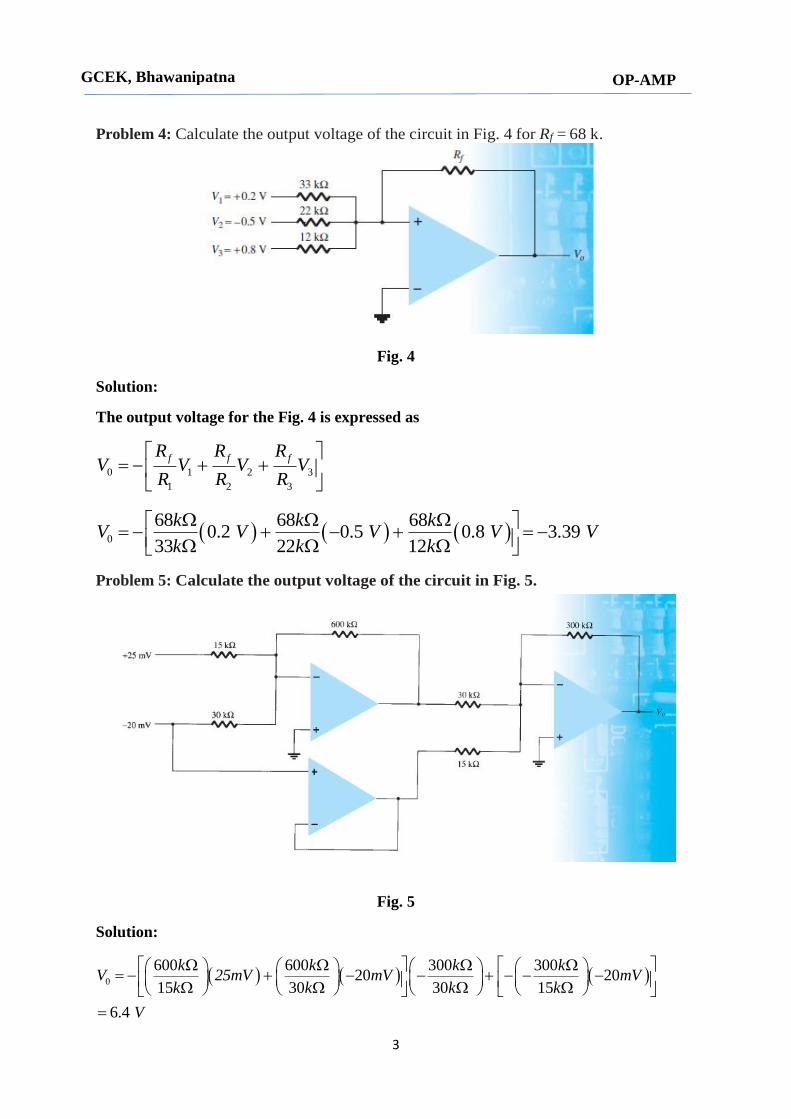
Problem 4: Calculate the output voltage of the circuit in Fig. 4 for Rf = 68 k.
Fig. 4
Solution:
The output voltage for the Fig. 4 is expressed as
0 1 2 3
1 2 3
f f fR R RV V V V
R R R
0
68 68 680.2 0.5 0.8 3.39
33 22 12
k k kV V V V V
k k k
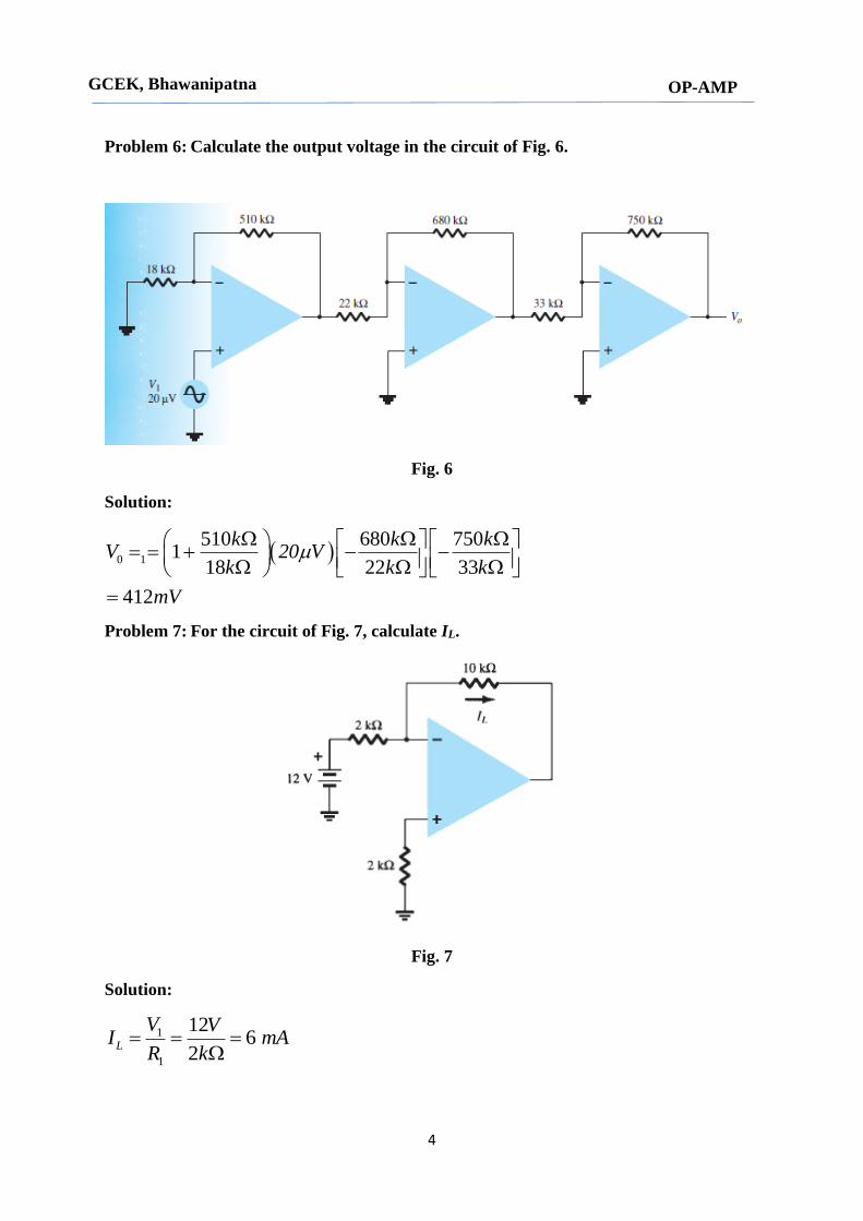
Problem 5: Calculate the output voltage of the circuit in Fig. 5.
Fig. 5
Solution:
0
600 600 300 30020 20
15 30 30 15
6.4
k k k kV 25mV mV mV
k k k k
V
4
GCEK, Bhawanipatna
OP-AMP
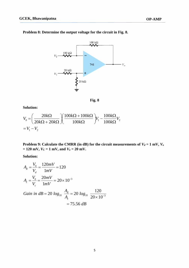
Problem 6: Calculate the output voltage in the circuit of Fig. 6.
Fig. 6
Solution:
0 1
510 680 7501
18 22 33
412
k k kV 20 V
k k k
mV
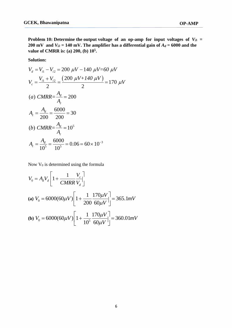
Problem 7: For the circuit of Fig. 7, calculate IL.
Fig. 7
Solution:
1
1
126
2L
V VI mA
R k
5
GCEK, Bhawanipatna
OP-AMP
Problem 8: Determine the output voltage for the circuit in Fig. 8.
Fig. 8
Solution:
0 1 2
1 2
20 100 100 100
20 20 100 100
k k k kV V V
k k k k
V V
Problem 9: Calculate the CMRR (in dB) for the circuit measurements of Vd = 1 mV, Vo
= 120 mV, VC = 1 mV, and Vo = 20 mV.
Solution:
0
30
10 10 3
120120
1
2020 10
1
12020 20
20 10
75.56
d
d
c
c
d
c
V mVA
V mV
V mVA
V mV
AGain in dB log log
A
dB
6
GCEK, Bhawanipatna
OP-AMP
Problem 10: Determine the output voltage of an op-amp for input voltages of Vi1 =
200 mV and Vi2 = 140 mV. The amplifier has a differential gain of Ad = 6000 and the
value of CMRR is: (a) 200, (b) 105.
Solution:
1 2
1 2
5
3
5 5
200 140
200170
2 2
( ) 200
600030
200 200
( ) 10
60000.06 60 10
10 10
d i i
i ic
d
c
dc
d
c
dc
V V V V V=60 V
V+140 VV VV V
Aa CMRR=
A
AA
Ab CMRR=
A
AA
Now V0 is determined using the formula
0
11 c
d d
d
VV A V
CMRR V
(a) 0
1 1706000(60 ) 1 365.1
200 60
VV V mV
V
(b) 0 5
1 1706000(60 ) 1 360.01
10 60
VV V mV
V


![Topic 7 Revision [143 marks]](https://static.fdocument.org/doc/165x107/616a52ca11a7b741a3513f24/topic-7-revision-143-marks.jpg)