STB11NK50Z - STP11NK50ZFP STP11NK50Z · Internal schematic diagram Type V DSS RDS(on) max ID Pw ......
16
May 2008 Rev 6 1/16 16 STB11NK50Z - STP11NK50ZFP STP11NK50Z N-channel 500 V, 0.48 Ω , 10 A TO-220, TO-220FP, D 2 PAK Zener-protected SuperMESH TM Power MOSFET Features ■ Extremely high dv/dt capability ■ 100% avalanche tested ■ Gate charge minimized ■ Very low intrinsic capacitances Application ■ Switching applications Description The SuperMESH™ series is obtained through an extreme optimization of ST’s well established strip-based PowerMESH™ layout. In addition to pushing on-resistance significantly down, special care is taken to ensure a very good dv/dt capability for the most demanding applications. Figure 1. Internal schematic diagram Type V DSS R DS(on) max I D Pw STB11NK50Z 500 V < 0.52 Ω 10 A 125 W STP11NK50ZFP 500 V < 0.52 Ω 10 A 30 W STP11NK50Z 500 V < 0.52 Ω 10 A 125 W TO-220FP TO-220 D 2 PAK 1 2 3 1 2 3 1 3 Table 1. Device summary Order codes Marking Package Packaging STB11NK50ZT4 B11NK50Z D²PAK Tape and reel STP11NK50ZFP P11NK50ZFP TO-220FP Tube STP11NK50Z P11NK50Z TO-220 Tube www.st.com
Transcript of STB11NK50Z - STP11NK50ZFP STP11NK50Z · Internal schematic diagram Type V DSS RDS(on) max ID Pw ......
May 2008 Rev 6 1/16
16
STB11NK50Z - STP11NK50ZFPSTP11NK50Z
N-channel 500 V, 0.48 Ω , 10 A TO-220, TO-220FP, D2PAKZener-protected SuperMESHTM Power MOSFET
Features
Extremely high dv/dt capability
100% avalanche tested
Gate charge minimized
Very low intrinsic capacitances
Application Switching applications
DescriptionThe SuperMESH™ series is obtained through an extreme optimization of ST’s well established strip-based PowerMESH™ layout. In addition to pushing on-resistance significantly down, special care is taken to ensure a very good dv/dt capability for the most demanding applications.
Figure 1. Internal schematic diagram
Type VDSSRDS(on)
maxID Pw
STB11NK50Z 500 V < 0.52 Ω 10 A 125 W
STP11NK50ZFP 500 V < 0.52 Ω 10 A 30 W
STP11NK50Z 500 V < 0.52 Ω 10 A 125 W TO-220FPTO-220
D2PAK
12
3
12
3
13
Table 1. Device summary
Order codes Marking Package Packaging
STB11NK50ZT4 B11NK50Z D²PAK Tape and reel
STP11NK50ZFP P11NK50ZFP TO-220FP Tube
STP11NK50Z P11NK50Z TO-220 Tube
www.st.com
Contents STB11NK50Z - STP11NK50ZFP - STP11NK50Z
2/16
Contents
1 Electrical ratings . . . . . . . . . . . . . . . . . . . . . . . . . . . . . . . . . . . . . . . . . . . . 3
2 Electrical characteristics . . . . . . . . . . . . . . . . . . . . . . . . . . . . . . . . . . . . . 5
2.1 Electrical characteristics (curves) . . . . . . . . . . . . . . . . . . . . . . . . . . . . . 7
3 Test circuit . . . . . . . . . . . . . . . . . . . . . . . . . . . . . . . . . . . . . . . . . . . . . . . 10
4 Package mechanical data . . . . . . . . . . . . . . . . . . . . . . . . . . . . . . . . . . . . 11
5 Packaging mechanical data . . . . . . . . . . . . . . . . . . . . . . . . . . . . . . . . . 15
6 Revision history . . . . . . . . . . . . . . . . . . . . . . . . . . . . . . . . . . . . . . . . . . . 16
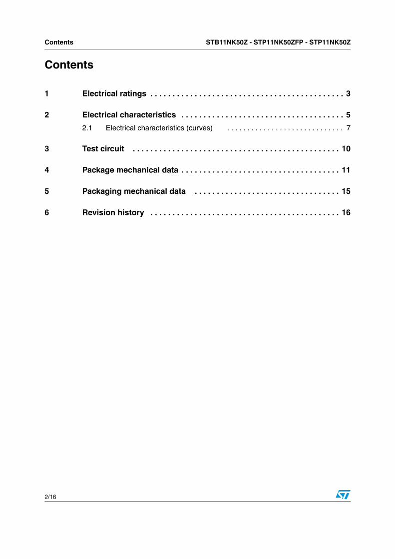
STB11NK50Z - STP11NK50ZFP - STP11NK50Z Electrical ratings
3/16
1 Electrical ratings
Table 2. Absolute maximum ratings
Symbol Parameter
Value
UnitTO-220
D²PAKTO-220FP
VDS Drain-source voltage (VGS = 0) 500 V
VGS Gate-source voltage ± 30 V
ID Drain current (continuous) at TC = 25 °C 10 10(1)
1. Limited only by maximum temperature allowed
A
ID Drain current (continuous) at TC=100 °C 6.3 6.3(1) A
IDM(2)
2. Pulse width limited by safe operating area
Drain current (pulsed) 40 40(1) A
PTOT Total dissipation at TC = 25 °C 125 30 W
Derating factor 1 0.24 W/°C
VESD(G-S)Gate source ESD (HBM-C= 100 pF,
R= 1.5 kΩ)4000 V
dv/dt(3)
3. ISD ≤ 10 A, di/dt ≤ 200 A/µs, VDD ≤ V(BR)DSS, Tj ≤ TJMAX.
Peak diode recovery voltage slope 4.5 V/ns
VISO Insulation withstand voltage (DC) -- 2500 V
TJ
Tstg
Operating junction temperature
Storage temperature-55 to 150 °C
Table 3. Thermal data
Symbol Parameter
Value
UnitTO-220
D²PAKTO-220FP
Rthj-case Thermal resistance junction-case max 1 4.2 °C/W
Rthj-a Thermal resistance junction-ambient max 62.5 °C/W
TlMaximum lead temperature for soldering purpose
300 °C
Table 4. Avalanche characteristics
Symbol Parameter Value Unit
IASAvalanche current, repetitive or not-repetitive (pulse width limited by Tj max)
10 A
EASSingle pulse avalanche energy
(starting TJ = 25 °C, ID=IAR, VDD = 50 V)190 mJ
Electrical characteristics STB11NK50Z - STP11NK50ZFP - STP11NK50Z
4/16
2 Electrical characteristics
(TCASE = 25 °C unless otherwise specified)
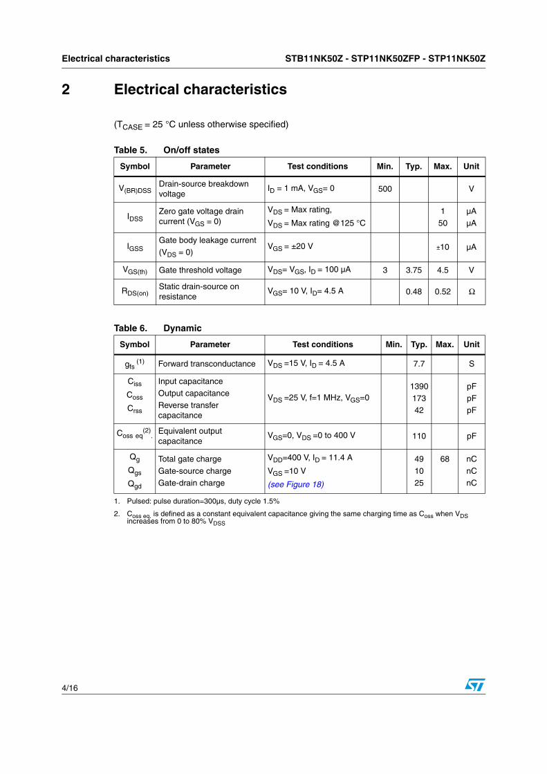
Table 5. On/off states
Symbol Parameter Test conditions Min. Typ. Max. Unit
V(BR)DSSDrain-source breakdown voltage
ID = 1 mA, VGS= 0 500 V
IDSSZero gate voltage drain current (VGS = 0)
VDS = Max rating,
VDS = Max rating @125 °C
1
50
µA
µA
IGSSGate body leakage current
(VDS = 0)VGS = ±20 V ±10 µA
VGS(th) Gate threshold voltage VDS= VGS, ID = 100 µA 3 3.75 4.5 V
RDS(on)Static drain-source on resistance
VGS= 10 V, ID= 4.5 A 0.48 0.52 Ω
Table 6. Dynamic
Symbol Parameter Test conditions Min. Typ. Max. Unit
gfs (1)
1. Pulsed: pulse duration=300µs, duty cycle 1.5%
Forward transconductance VDS =15 V, ID = 4.5 A 7.7 S
Ciss
Coss
Crss
Input capacitance
Output capacitance
Reverse transfer capacitance
VDS =25 V, f=1 MHz, VGS=01390
17342
pF
pFpF
Coss eq(2)
.
2. Coss eq. is defined as a constant equivalent capacitance giving the same charging time as Coss when VDS increases from 0 to 80% VDSS
Equivalent output capacitance
VGS=0, VDS =0 to 400 V 110 pF
Qg
Qgs
Qgd
Total gate charge
Gate-source charge
Gate-drain charge
VDD=400 V, ID = 11.4 A
VGS =10 V
(see Figure 18)
49
10
25
68 nC
nC
nC
STB11NK50Z - STP11NK50ZFP - STP11NK50Z Electrical characteristics
5/16
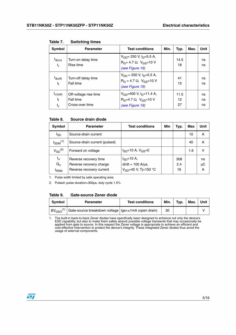
Table 7. Switching times
Symbol Parameter Test conditions Min. Typ. Max. Unit
td(on)
tr
Turn-on delay time
Rise time
VDD= 250 V, ID=5.5 A,
RG= 4.7 Ω, VGS=10 V
(see Figure 19)
14.5
18
ns
ns
td(off)
tf
Turn-off delay timeFall time
VDD = 250 V, ID=5.5 A,
RG = 4.7 Ω, VGS=10 V
(see Figure 19)
4115
nsns
tr(Voff)
tftc
Off-voltage rise timeFall time
Cross-over time
VDD=400 V, ID=11.4 A,
RG=4.7 Ω, VGS=10 V
(see Figure 19)
11.512
27
nsns
ns
Table 8. Source drain diode
Symbol Parameter Test conditions Min Typ. Max Unit
ISD Source-drain current 10 A
ISDM(1)
1. Pulse width limited by safe operating area
Source-drain current (pulsed) 40 A
VSD(2)
2. Pulsed: pulse duration=300µs, duty cycle 1.5%
Forward on voltage ISD=10 A, VGS=0 1.6 V
trrQrr
IRRM
Reverse recovery time
Reverse recovery charge
Reverse recovery current
ISD=10 A,
di/dt = 100 A/µs,
VDD=45 V, Tj=150 °C
308
2.4
16
ns
µC
A
Table 9. Gate-source Zener diode
Symbol Parameter Test conditions Min. Typ. Max. Unit
BVGSO(1)
1. The built-in back-to-back Zener diodes have specifically been designed to enhance not only the device’s ESD capability, but also to make them safely absorb possible voltage transients that may occasionally be applied from gate to source. In this respect the Zener voltage is appropriate to achieve an efficient and cost-effective intervention to protect the device’s integrity. These integrated Zener diodes thus avoid the usage of external components.
Gate-source breakdown voltage Igs=±1mA (open drain) 30 V
Electrical characteristics STB11NK50Z - STP11NK50ZFP - STP11NK50Z
6/16
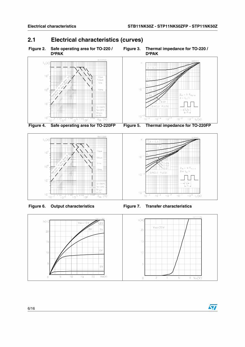
2.1 Electrical characteristics (curves) Figure 2. Safe operating area for TO-220 /
D²PAKFigure 3. Thermal impedance for TO-220 /
D²PAK
Figure 4. Safe operating area for TO-220FP Figure 5. Thermal impedance for TO-220FP
Figure 6. Output characteristics Figure 7. Transfer characteristics
STB11NK50Z - STP11NK50ZFP - STP11NK50Z Electrical characteristics
7/16
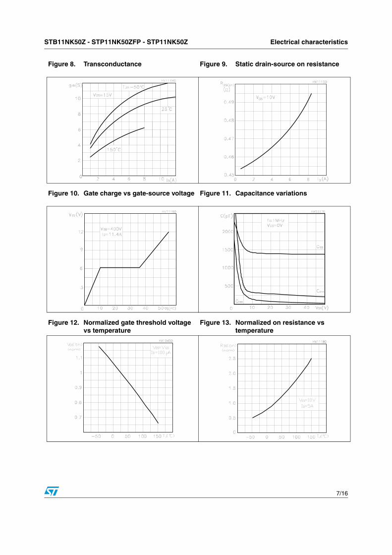
Figure 8. Transconductance Figure 9. Static drain-source on resistance
Figure 10. Gate charge vs gate-source voltage Figure 11. Capacitance variations
Figure 12. Normalized gate threshold voltage vs temperature
Figure 13. Normalized on resistance vs temperature
Electrical characteristics STB11NK50Z - STP11NK50ZFP - STP11NK50Z
8/16
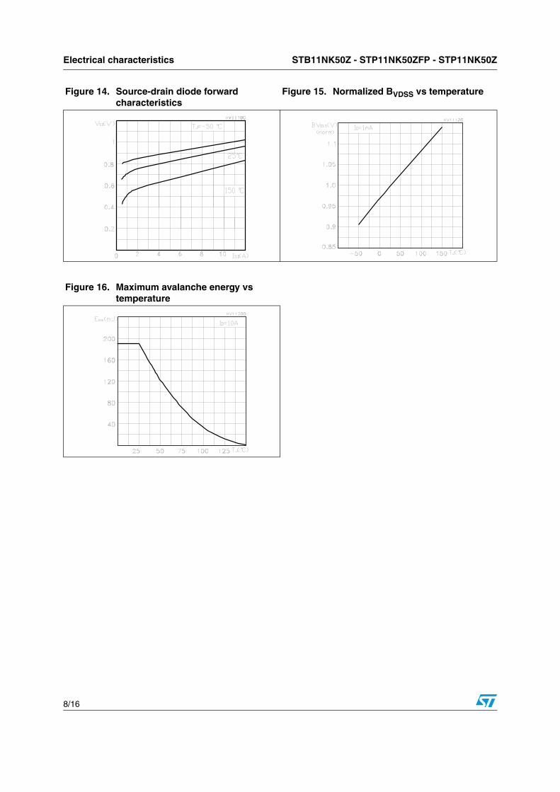
Figure 14. Source-drain diode forward characteristics
Figure 15. Normalized BVDSS vs temperature
Figure 16. Maximum avalanche energy vs temperature
STB11NK50Z - STP11NK50ZFP - STP11NK50Z Test circuit
9/16
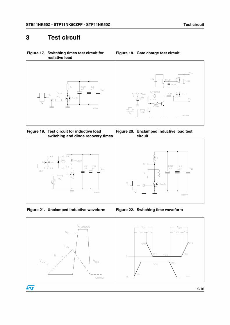
3 Test circuit
Figure 17. Switching times test circuit for resistive load
Figure 18. Gate charge test circuit
Figure 19. Test circuit for inductive load switching and diode recovery times
Figure 20. Unclamped Inductive load test circuit
Figure 21. Unclamped inductive waveform Figure 22. Switching time waveform
Package mechanical data STB11NK50Z - STP11NK50ZFP - STP11NK50Z
10/16
4 Package mechanical data
In order to meet environmental requirements, ST offers these devices in ECOPACK® packages. These packages have a lead-free second level interconnect. The category of second level interconnect is marked on the package and on the inner box label, in compliance with JEDEC Standard JESD97. The maximum ratings related to soldering conditions are also marked on the inner box label. ECOPACK is an ST trademark. ECOPACK specifications are available at: www.st.com
STB11NK50Z - STP11NK50ZFP - STP11NK50Z Package mechanical data
11/16
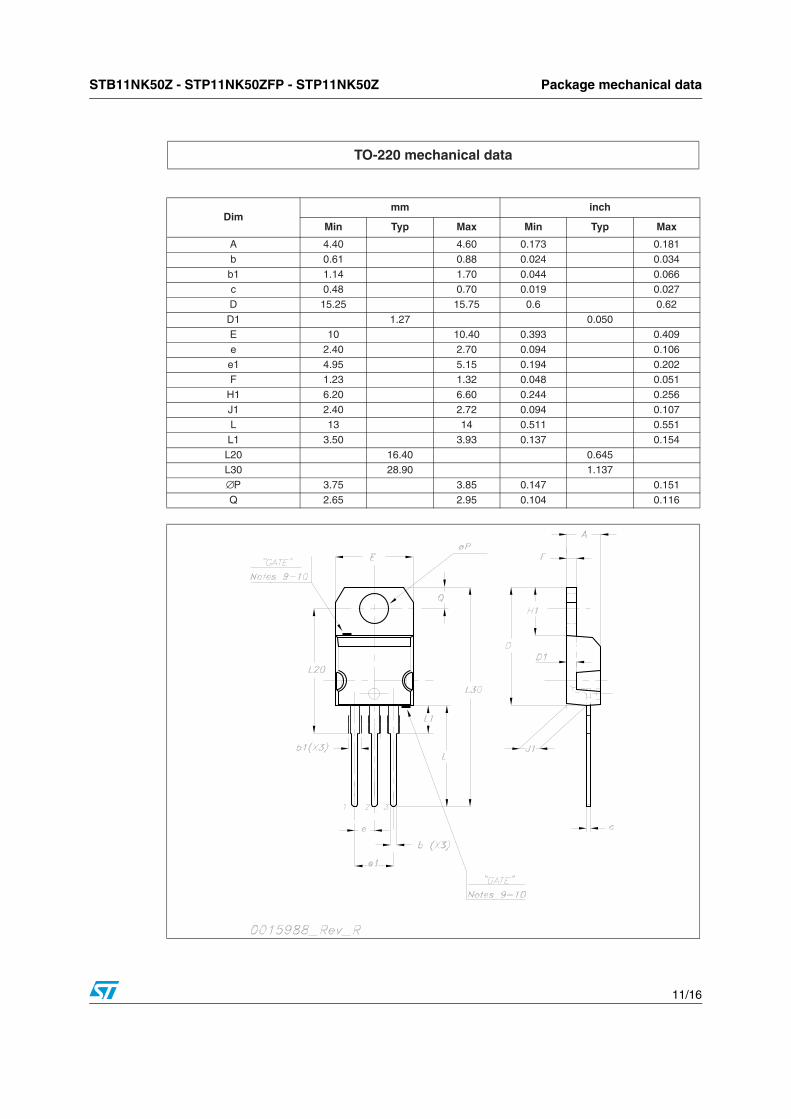
TO-220 mechanical data
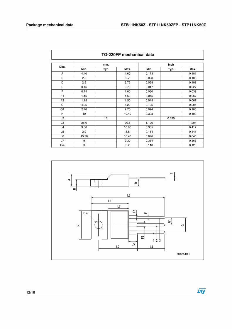
Dimmm inch
Min Typ Max Min Typ Max
A 4.40 4.60 0.173 0.181
b 0.61 0.88 0.024 0.034
b1 1.14 1.70 0.044 0.066c 0.48 0.70 0.019 0.027
D 15.25 15.75 0.6 0.62
D1 1.27 0.050E 10 10.40 0.393 0.409
e 2.40 2.70 0.094 0.106
e1 4.95 5.15 0.194 0.202F 1.23 1.32 0.048 0.051
H1 6.20 6.60 0.244 0.256
J1 2.40 2.72 0.094 0.107L 13 14 0.511 0.551
L1 3.50 3.93 0.137 0.154
L20 16.40 0.645L30 28.90 1.137
∅P 3.75 3.85 0.147 0.151
Q 2.65 2.95 0.104 0.116
Package mechanical data STB11NK50Z - STP11NK50ZFP - STP11NK50Z
12/16
Dim.mm. inch
Min. Typ Max. Min. Typ. Max.
A 4.40 4.60 0.173 0.181
B 2.5 2.7 0.098 0.106
D 2.5 2.75 0.098 0.108
E 0.45 0.70 0.017 0.027
F 0.75 1.00 0.030 0.039
F1 1.15 1.50 0.045 0.067
F2 1.15 1.50 0.045 0.067
G 4.95 5.20 0.195 0.204
G1 2.40 2.70 0.094 0.106
H 10 10.40 0.393 0.409
L2 16 0.630
L3 28.6 30.6 1.126 1.204
L4 9.80 10.60 0.385 0.417
L5 2.9 3.6 0.114 0.141
L6 15.90 16.40 0.626 0.645
L7 9 9.30 0.354 0.366
Dia 3 3.2 0.118 0.126
TO-220FP mechanical data
L2
A
B
D
E
H G
L6
F
L3
G1
1 2 3
F2
F1
L7
L4L5
7012510-I
Dia
STB11NK50Z - STP11NK50ZFP - STP11NK50Z Package mechanical data
13/16
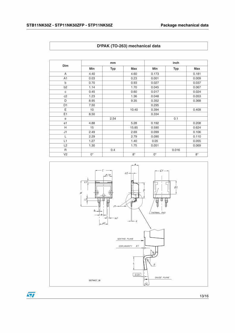
D²PAK (TO-263) mechanical data
Dimmm inch
Min Typ Max Min Typ Max
A 4.40 4.60 0.173 0.181
A1 0.03 0.23 0.001 0.009
b 0.70 0.93 0.027 0.037b2 1.14 1.70 0.045 0.067
c 0.45 0.60 0.017 0.024
c2 1.23 1.36 0.048 0.053D 8.95 9.35 0.352 0.368
D1 7.50 0.295
E 10 10.40 0.394 0.409E1 8.50 0.334
e 2.54 0.1
e1 4.88 5.28 0.192 0.208H 15 15.85 0.590 0.624
J1 2.49 2.69 0.099 0.106
L 2.29 2.79 0.090 0.110L1 1.27 1.40 0.05 0.055
L2 1.30 1.75 0.051 0.069
R 0.4 0.016V2 0° 8° 0° 8°
0079457_M
Packaging mechanical data STB11NK50Z - STP11NK50ZFP - STP11NK50Z
14/16
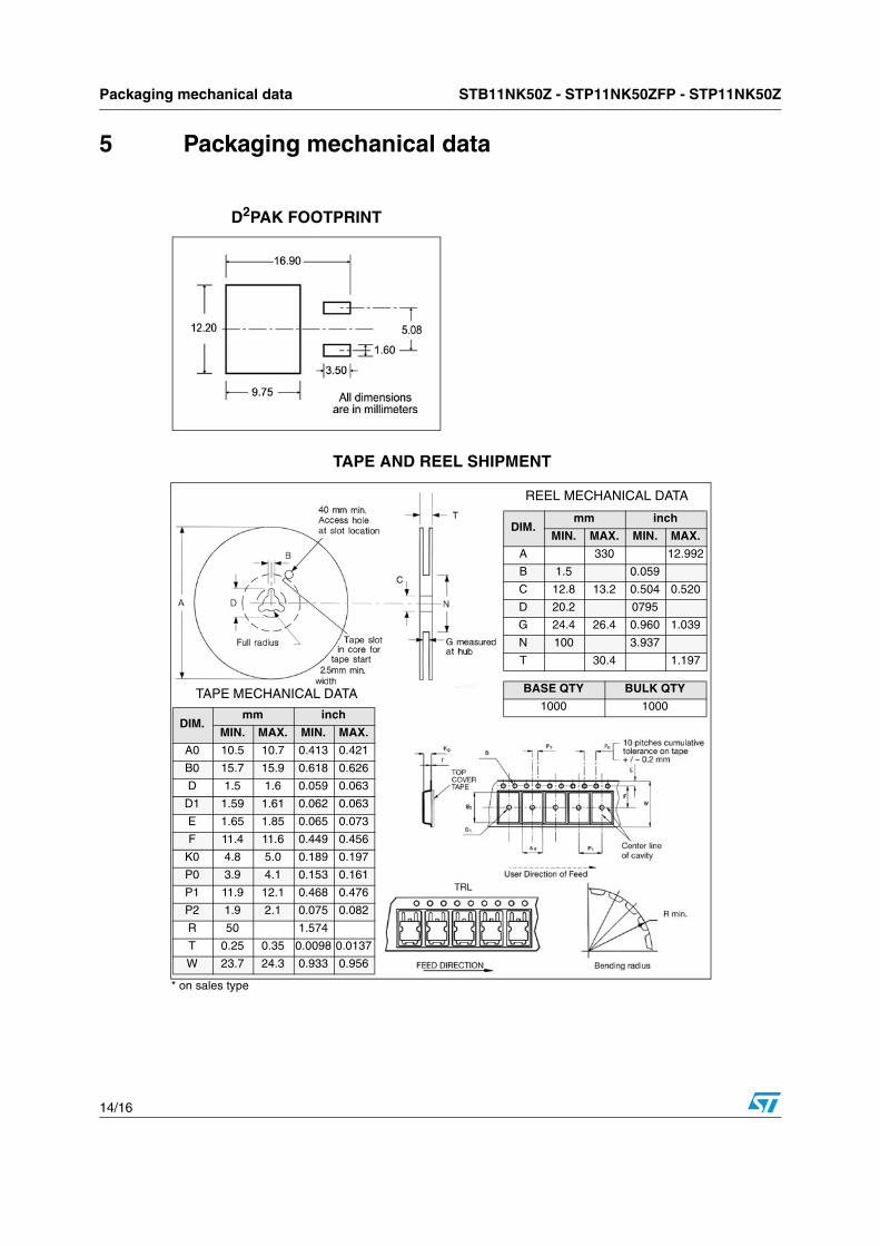
5 Packaging mechanical data
TAPE AND REEL SHIPMENT
D2PAK FOOTPRINT
* on sales type
DIM.mm inch
MIN. MAX. MIN. MAX.
A 330 12.992
B 1.5 0.059
C 12.8 13.2 0.504 0.520
D 20.2 0795
G 24.4 26.4 0.960 1.039
N 100 3.937
T 30.4 1.197
BASE QTY BULK QTY
1000 1000
REEL MECHANICAL DATA
DIM.mm inch
MIN. MAX. MIN. MAX.
A0 10.5 10.7 0.413 0.421
B0 15.7 15.9 0.618 0.626
D 1.5 1.6 0.059 0.063
D1 1.59 1.61 0.062 0.063
E 1.65 1.85 0.065 0.073
F 11.4 11.6 0.449 0.456
K0 4.8 5.0 0.189 0.197
P0 3.9 4.1 0.153 0.161
P1 11.9 12.1 0.468 0.476
P2 1.9 2.1 0.075 0.082
R 50 1.574
T 0.25 0.35 0.0098 0.0137
W 23.7 24.3 0.933 0.956
TAPE MECHANICAL DATA
STB11NK50Z - STP11NK50ZFP - STP11NK50Z Revision history
15/16
6 Revision history
Table 10. Revision history
Date Revision Changes
08-Sep-2005 3 Complete version with curves
14-Oct-2005 4 Inserted ecopack indication
26-Mar-2006 5 New template, no content change
29-Apr-2008 6 IGSS value changed in Table 6
STB11NK50Z - STP11NK50ZFP - STP11NK50Z
16/16
Please Read Carefully:
Information in this document is provided solely in connection with ST products. STMicroelectronics NV and its subsidiaries (“ST”) reserve theright to make changes, corrections, modifications or improvements, to this document, and the products and services described herein at anytime, without notice.
All ST products are sold pursuant to ST’s terms and conditions of sale.
Purchasers are solely responsible for the choice, selection and use of the ST products and services described herein, and ST assumes noliability whatsoever relating to the choice, selection or use of the ST products and services described herein.
No license, express or implied, by estoppel or otherwise, to any intellectual property rights is granted under this document. If any part of thisdocument refers to any third party products or services it shall not be deemed a license grant by ST for the use of such third party productsor services, or any intellectual property contained therein or considered as a warranty covering the use in any manner whatsoever of suchthird party products or services or any intellectual property contained therein.
UNLESS OTHERWISE SET FORTH IN ST’S TERMS AND CONDITIONS OF SALE ST DISCLAIMS ANY EXPRESS OR IMPLIEDWARRANTY WITH RESPECT TO THE USE AND/OR SALE OF ST PRODUCTS INCLUDING WITHOUT LIMITATION IMPLIEDWARRANTIES OF MERCHANTABILITY, FITNESS FOR A PARTICULAR PURPOSE (AND THEIR EQUIVALENTS UNDER THE LAWSOF ANY JURISDICTION), OR INFRINGEMENT OF ANY PATENT, COPYRIGHT OR OTHER INTELLECTUAL PROPERTY RIGHT.
UNLESS EXPRESSLY APPROVED IN WRITING BY AN AUTHORIZED ST REPRESENTATIVE, ST PRODUCTS ARE NOTRECOMMENDED, AUTHORIZED OR WARRANTED FOR USE IN MILITARY, AIR CRAFT, SPACE, LIFE SAVING, OR LIFE SUSTAININGAPPLICATIONS, NOR IN PRODUCTS OR SYSTEMS WHERE FAILURE OR MALFUNCTION MAY RESULT IN PERSONAL INJURY,DEATH, OR SEVERE PROPERTY OR ENVIRONMENTAL DAMAGE. ST PRODUCTS WHICH ARE NOT SPECIFIED AS "AUTOMOTIVEGRADE" MAY ONLY BE USED IN AUTOMOTIVE APPLICATIONS AT USER’S OWN RISK.
Resale of ST products with provisions different from the statements and/or technical features set forth in this document shall immediately voidany warranty granted by ST for the ST product or service described herein and shall not create or extend in any manner whatsoever, anyliability of ST.
ST and the ST logo are trademarks or registered trademarks of ST in various countries.
Information in this document supersedes and replaces all information previously supplied.
The ST logo is a registered trademark of STMicroelectronics. All other names are the property of their respective owners.
© 2008 STMicroelectronics - All rights reserved
STMicroelectronics group of companies
Australia - Belgium - Brazil - Canada - China - Czech Republic - Finland - France - Germany - Hong Kong - India - Israel - Italy - Japan - Malaysia - Malta - Morocco - Singapore - Spain - Sweden - Switzerland - United Kingdom - United States of America
www.st.com

![m-[n-]-Xyhpw tNI-∂q¿ aue-hn-bpsS {KŸ-߃! Janadhipathyavum.pdf · ... Kozhikode. Price: ... Xy-hm-Zn-Iƒ°pw Dƒs°m-≈m-\mhpw F∂n-cn-s°, Jp¿-B\pw P\m-[n-]-Xyhpw ]c-kv]](https://static.fdocument.org/doc/165x107/5b0e22297f8b9a8b038eac92/m-n-xyhpw-tni-q-aue-hn-bpss-ky-f-janadhipathyavumpdf-kozhikode-price.jpg)