Solid State Theory Physics 545 - Bilkent Universitygulseren/phys545/pdf/bands3.pdf · for each...
32
Solid State Theory Solid State Theory Physics 545 Physics 545 Band Theory III
Transcript of Solid State Theory Physics 545 - Bilkent Universitygulseren/phys545/pdf/bands3.pdf · for each...
Solid State TheorySolid State TheoryPhysics 545Physics 545
Band Theory III
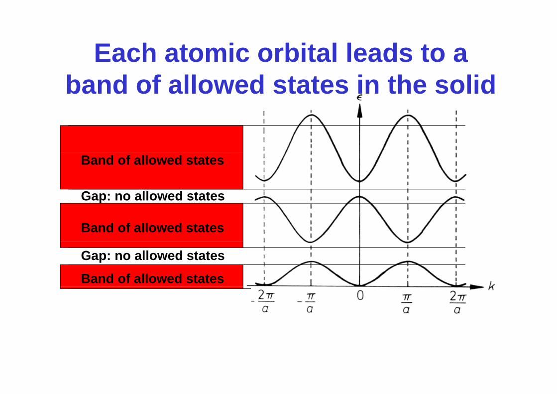
Each atomic orbital leads to a band of allowed states in the solid
Band of allowed states
Gap: no allowed states
Band of allowed states
Gap: no allowed states
Band of allowed states
Gap: no allowed states
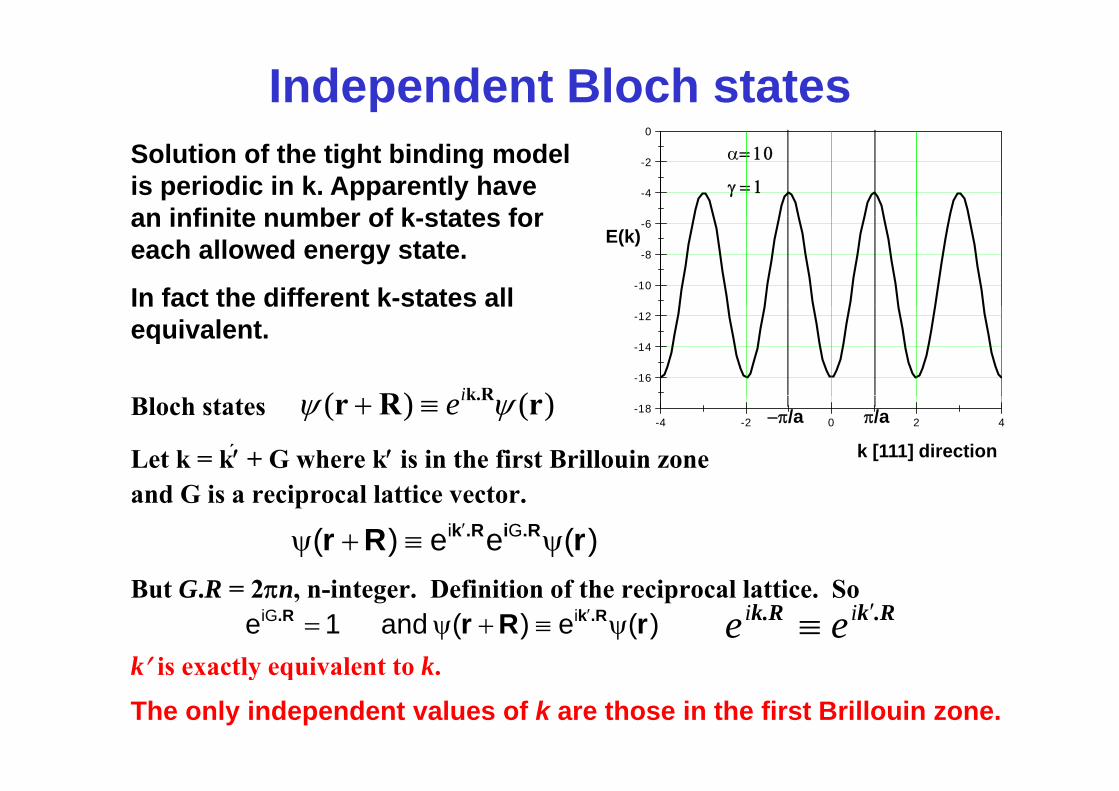
Independent Bloch states F1
-4
-2
0
α= 10
γ = 1
Solution of the tight binding model is periodic in k. Apparently have an infinite number of k states for
-10
-8
-6E(k)
an infinite number of k-states for each allowed energy state.
In fact the different k-states all
)()( R k Ri-16
-14
-12In fact the different k states all equivalent.
Bloch states
Let k = k ́′ + G where k′ is in the first Brillouin zoned G i i l l i
)()( rRr k.Rψψ ie≡+-4 -2 0 2 4
-18
k [111] direction
π/a−π/a
and G is a reciprocal lattice vector.
)(ee)( Gi rRr .Ri.Rk ψ≡+ψ ′
But G.R = 2πn, n-integer. Definition of the reciprocal lattice. So
k′ is exactly equivalent to k)(e)( and 1e iiG rRr .Rk.R ψ≡+ψ= ′ .Rkk.R ′≡ ii ee
k is exactly equivalent to k.
The only independent values of k are those in the first Brillouin zone.
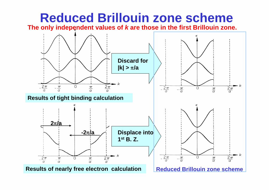
Reduced Brillouin zone schemeThe only independent values of k are those in the first Brillouin zone.y p
Discard for |k| > π/a
Results of tight binding calculation
Displace into 1st B Z
-2π/a2π/a
1st B. Z.
Results of nearly free electron calculation Reduced Brillouin zone scheme
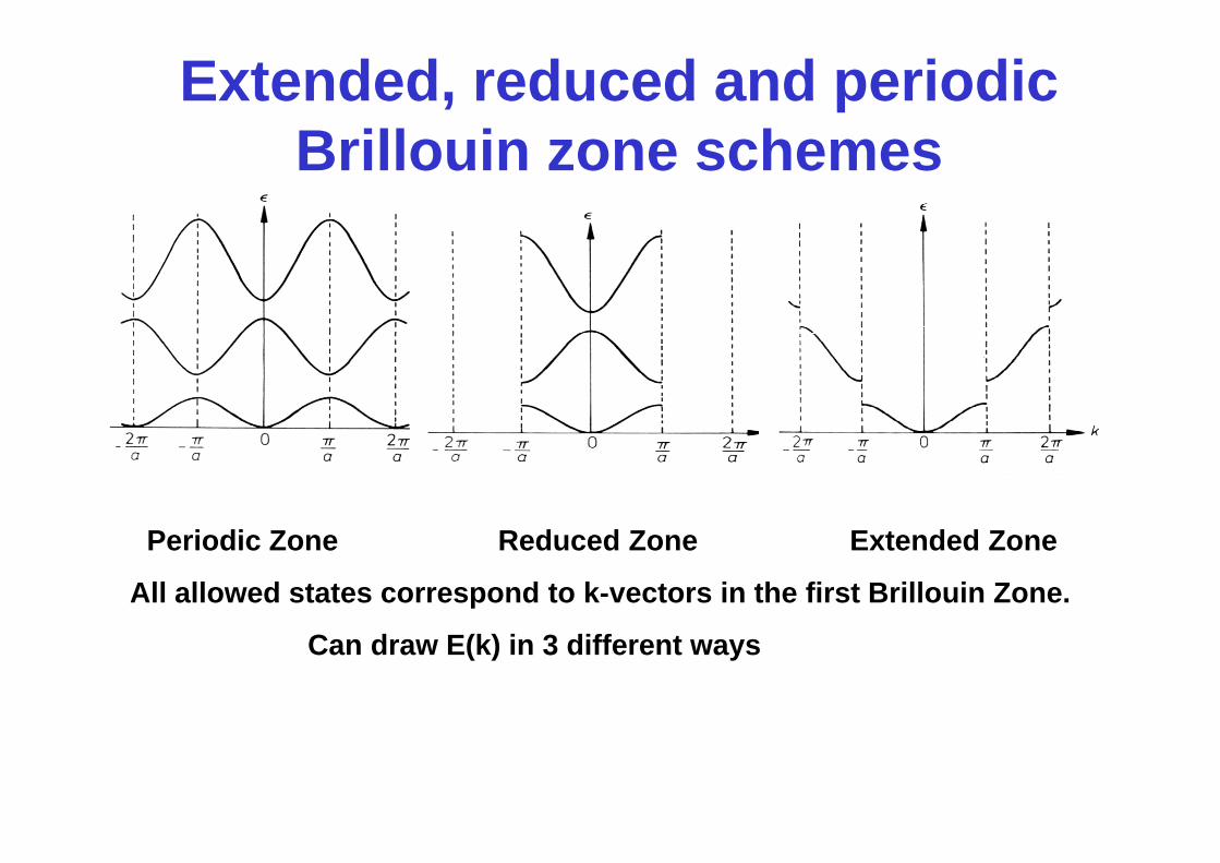
Extended, reduced and periodic B ill i hBrillouin zone schemes
P i di Z R d d Z E d d ZPeriodic Zone Reduced Zone Extended Zone
All allowed states correspond to k-vectors in the first Brillouin Zone.
Can draw E(k) in 3 different ways
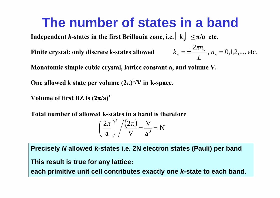
The number of states in a bandIndependent k-states in the first Brillouin zone, i.e. ⏐kx⏐ < π/a etc.
Finite crystal: only discrete k-states allowed .etc,....2,1,0,2
=±= xx
x nn
kπ
Finite crystal: only discrete k states allowed
Monatomic simple cubic crystal, lattice constant a, and volume V.
.etc,....,,0, xx nL
k
One allowed k state per volume (2π)3/V in k-space.
Volume of first BZ is (2π/a)3Volume of first BZ is (2π/a)
Total number of allowed k-states in a band is therefore( ) V22 3
⎞⎛ ( ) NaV
V2
a2
3 ==π
⎟⎠⎞
⎜⎝⎛ π
Precisely N allowed k-states i.e. 2N electron states (Pauli) per band
This result is true for any lattice: each primitive unit cell contributes exactly one k-state to each band.
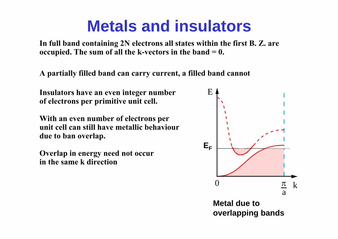
Metals and insulatorsIn full band containing 2N electrons all states within the first B. Z. are occupied. The sum of all the k-vectors in the band = 0.
A partially filled band can carry current, a filled band cannot
Insulators have an even integer number EInsulators have an even integer numberof electrons per primitive unit cell.
With an even number of electrons per
E
With an even number of electrons perunit cell can still have metallic behaviourdue to ban overlap.
EFOverlap in energy need not occurin the same k direction
EF
k0 πa
M t l d tMetal due to overlapping bands
E
E
E
EF
E
k0 π k0 πa
k0 πa
a
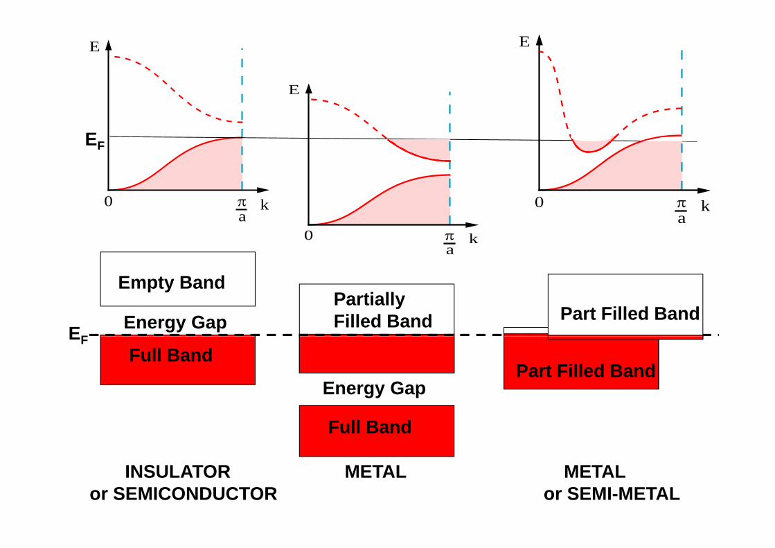
Empty Band
Energy GapPartially Filled Band Part Filled Band
EFFull Band
Energy GapPart Filled Band
EF
Full Band
INSULATOR METAL METALor SEMICONDUCTOR or SEMI-METAL
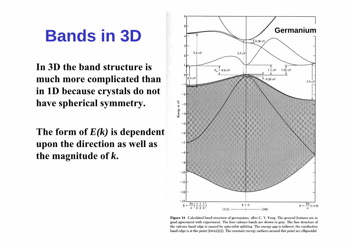
Bands in 3D GermaniumGermaniumBands in 3D In 3D the band structure isIn 3D the band structure is much more complicated than in 1D because crystals do not Figure removed to
reduce file sizeyhave spherical symmetry. reduce file size
The form of E(k) is dependent upon the direction as well as the magnitude of k.
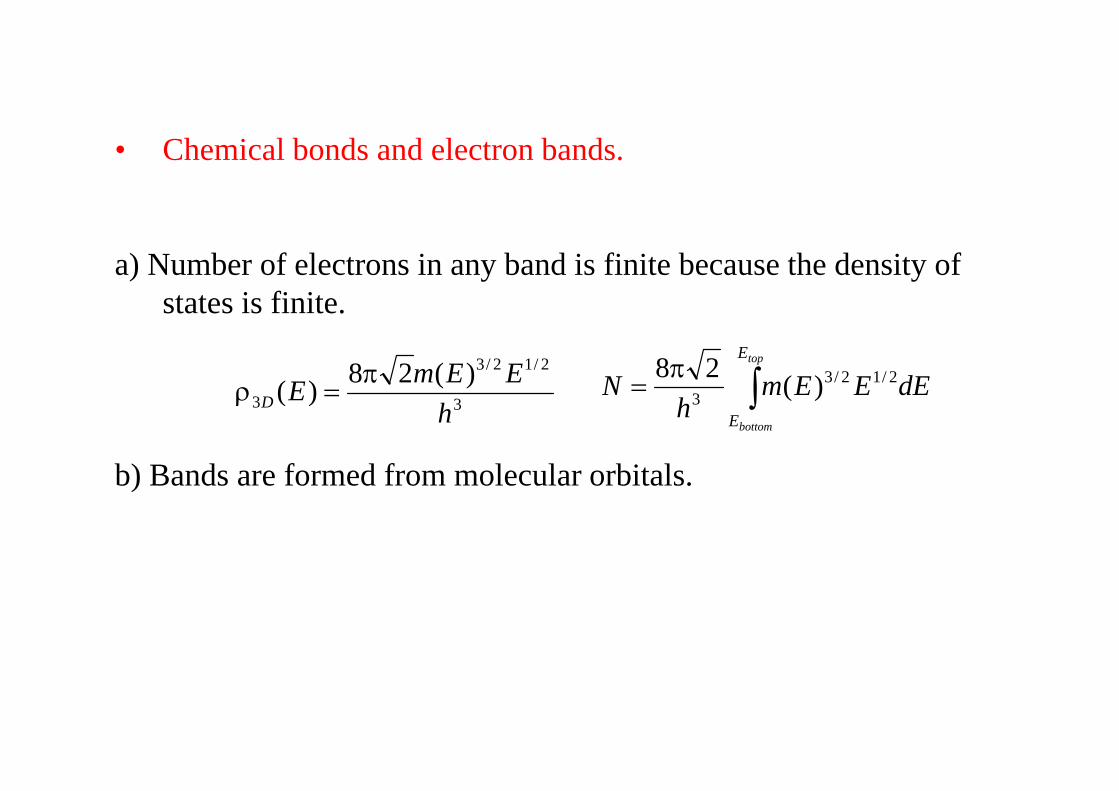
• Chemical bonds and electron bands.
a) Number of electrons in any band is finite because the density of states is finitestates is finite.
2/12/3)(28)( EEmE π=ρ ∫
π=
topE
dEEEmN 2/12/33 )(28
b) Bands are formed from molecular orbitals.
33 )(h
ED =ρ ∫bottomEh3 )(
b) Bands are formed from molecular orbitals.
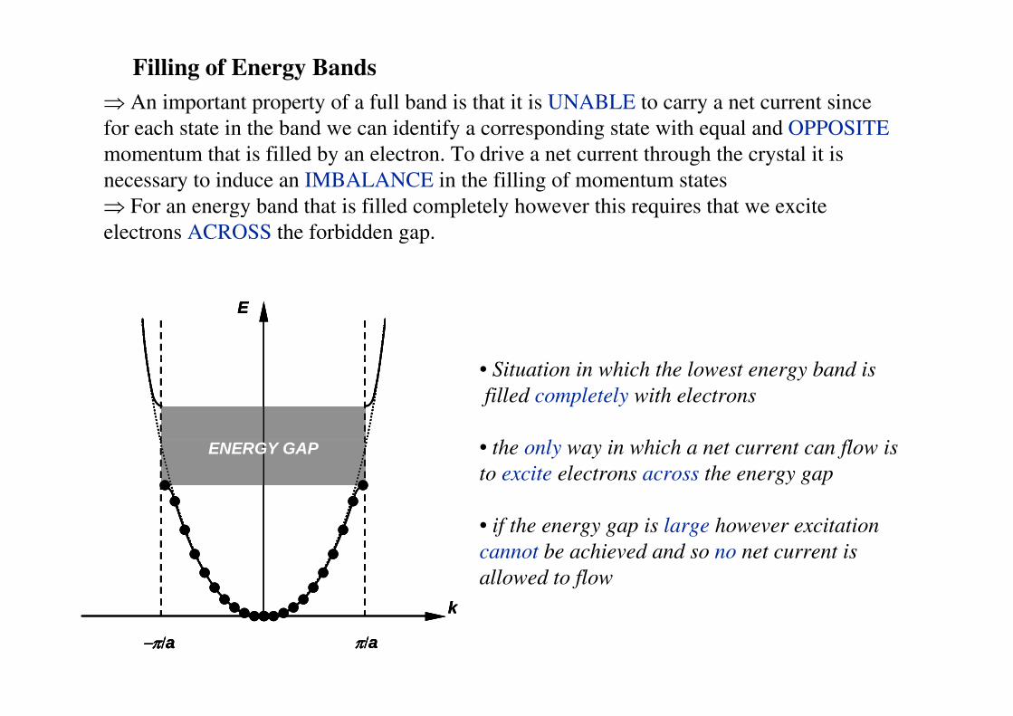
Filling of Energy Bands⇒ An important property of a full band is that it is UNABLE to carry a net current since for each state in the band we can identify a corresponding state with equal and OPPOSITEmomentum that is filled by an electron. To drive a net current through the crystal it is necessary to induce an IMBALANCE in the filling of momentum states ⇒ For an energy band that is filled completely however this requires that we excite electrons ACROSS the forbidden gap.
EEE
• Situation in which the lowest energy band isfilled completely with electrons
h l h h l• the only way in which a net current can flow isto excite electrons across the energy gap
if th i l h it ti
ENERGY GAPENERGY GAPENERGY GAP
• if the energy gap is large however excitationcannot be achieved and so no net current isallowed to flow
kkkk
π/a−π/a
k
π/a−π/a
k
π/a−π/a
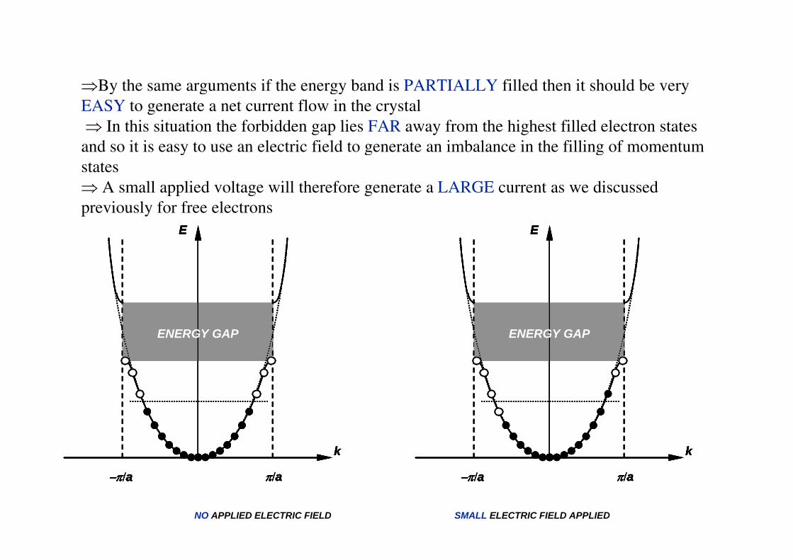
⇒By the same arguments if the energy band is PARTIALLY filled then it should be very ⇒By the same arguments if the energy band is PARTIALLY filled then it should be very EASY to generate a net current flow in the crystal⇒ In this situation the forbidden gap lies FAR away from the highest filled electron states and so it is easy to use an electric field to generate an imbalance in the filling of momentum y g gstates⇒ A small applied voltage will therefore generate a LARGE current as we discussed previously for free electrons
E EEEE EEE
ENERGY GAP ENERGY GAPENERGY GAPENERGY GAPENERGY GAP ENERGY GAPENERGY GAPENERGY GAP
k kkkk kkk
π/a−π/a π/a−π/aπ/a−π/a π/a−π/a π/a−π/a π/a−π/a π/a−π/a π/a−π/a
NO APPLIED ELECTRIC FIELD SMALL ELECTRIC FIELD APPLIED
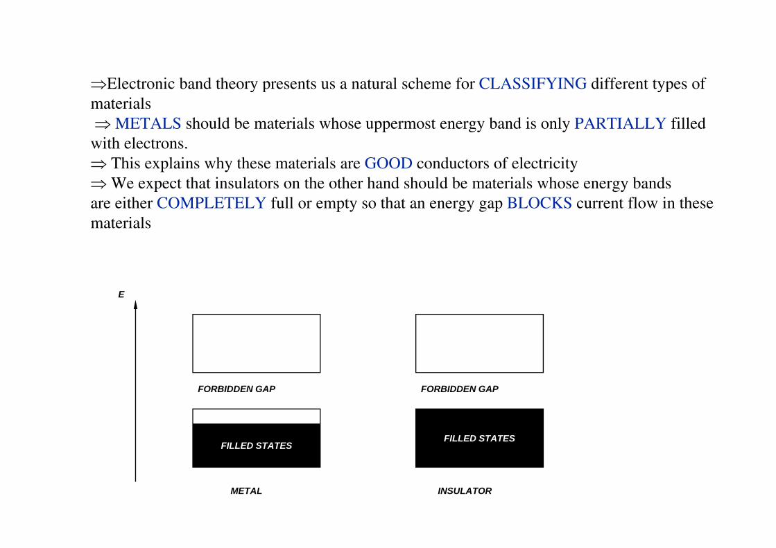
⇒Electronic band theory presents us a natural scheme for CLASSIFYING different types of ⇒Electronic band theory presents us a natural scheme for CLASSIFYING different types of materials⇒ METALS should be materials whose uppermost energy band is only PARTIALLY filled with electrons.⇒ This explains why these materials are GOOD conductors of electricity⇒ We expect that insulators on the other hand should be materials whose energy bandsare either COMPLETELY full or empty so that an energy gap BLOCKS current flow in these materials
E
FORBIDDEN GAP FORBIDDEN GAP
FILLED STATESFILLED STATES
METAL INSULATOR
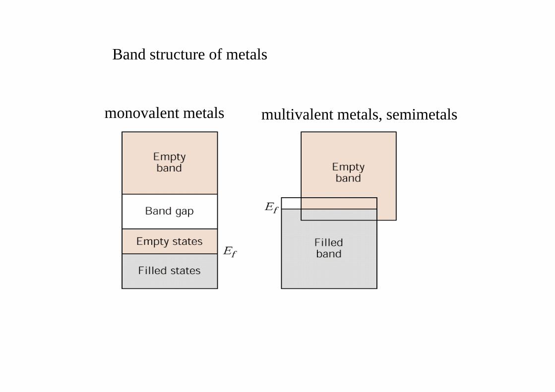
Band structure of metals
l lmonovalent metals multivalent metals, semimetals
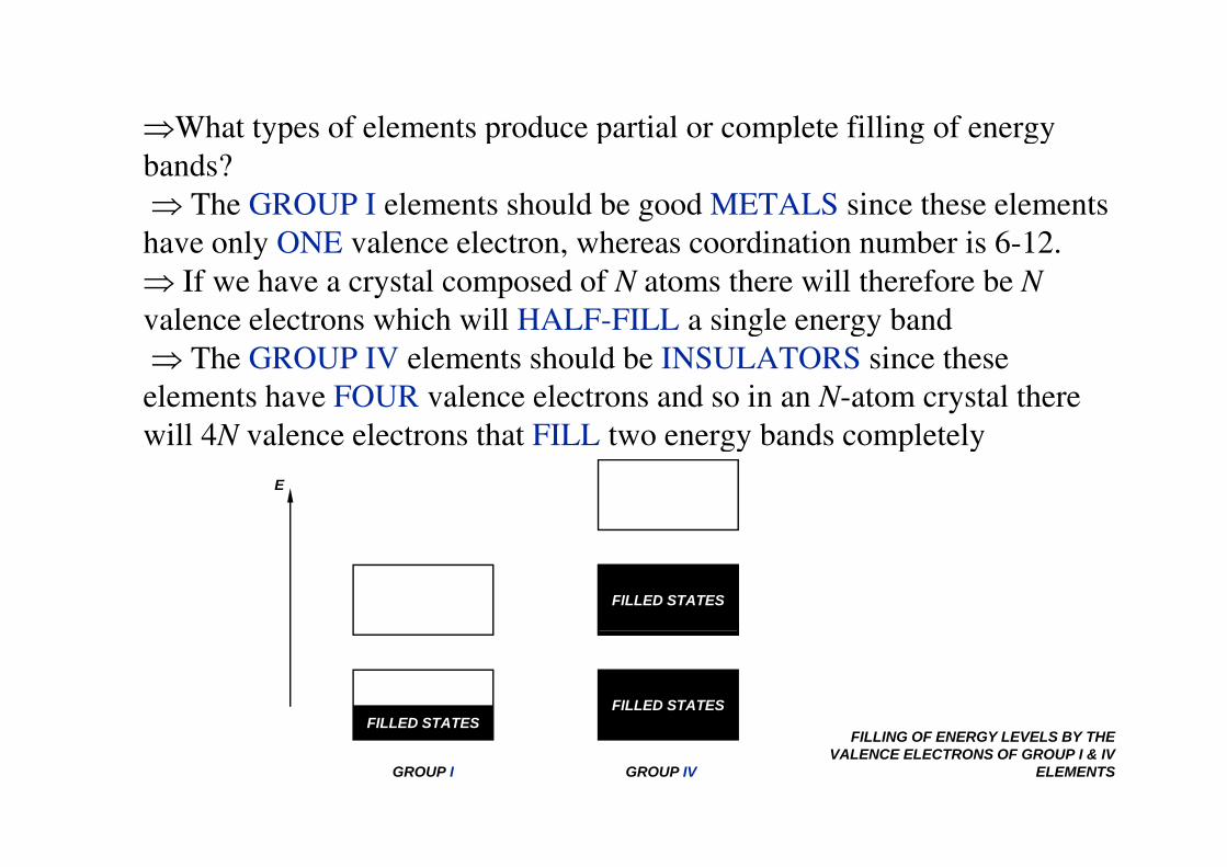
⇒What types of elements produce partial or complete filling of energy yp p p p g gybands?⇒ The GROUP I elements should be good METALS since these elements h l ONE l l t h di ti b i 6 12 have only ONE valence electron, whereas coordination number is 6-12. ⇒ If we have a crystal composed of N atoms there will therefore be Nvalence electrons which will HALF-FILL a single energy bandg gy⇒ The GROUP IV elements should be INSULATORS since these elements have FOUR valence electrons and so in an N-atom crystal there will 4N valence electrons that FILL two energy bands completelywill 4N valence electrons that FILL two energy bands completely
E
FILLED STATES
FILLED STATESFILLED STATES
GROUP I GROUP IV
FILLING OF ENERGY LEVELS BY THEVALENCE ELECTRONS OF GROUP I & IV
ELEMENTS
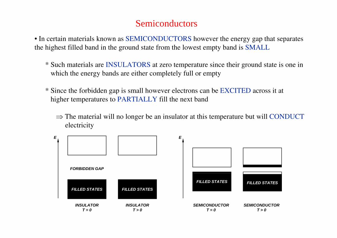
• In certain materials known as SEMICONDUCTORS however the energy gap that separates
Semiconductors• In certain materials known as SEMICONDUCTORS however the energy gap that separates the highest filled band in the ground state from the lowest empty band is SMALL
* Such materials are INSULATORS at zero temperature since their ground state is one in Such materials are INSULATORS at zero temperature since their ground state is one inwhich the energy bands are either completely full or empty
* Since the forbidden gap is small however electrons can be EXCITED across it at Since the forbidden gap is small however electrons can be EXCITED across it at higher temperatures to PARTIALLY fill the next band
⇒ The material will no longer be an insulator at this temperature but will CONDUCTg pelectricity
E E
FORBIDDEN GAP
FILLED STATES FILLED STATES
FILLED STATES FILLED STATES
INSULATORT = 0
INSULATORT > 0
SEMICONDUCTORT = 0
SEMICONDUCTORT > 0
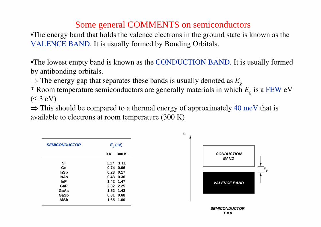
Some general COMMENTS on semiconductors•The energy band that holds the valence electrons in the ground state is known as the The energy band that holds the valence electrons in the ground state is known as the VALENCE BAND. It is usually formed by Bonding Orbitals.
•The lowest empty band is known as the CONDUCTION BAND It is usually formed •The lowest empty band is known as the CONDUCTION BAND. It is usually formed by antibonding orbitals.⇒ The energy gap that separates these bands is usually denoted as Eg
* R t t i d t ll t i l i hi h E i FEW V * Room temperature semiconductors are generally materials in which Eg is a FEW eV (≤ 3 eV)⇒ This should be compared to a thermal energy of approximately 40 meV that is available to electrons at room temperature (300 K)
E
SEMICONDUCTOR
Si
Eg (eV)
0 K 300 K
1.17 1.11
CONDUCTIONBAND
GeInSbInAsInPGaP
GaAs
0.74 0.660.23 0.170.43 0.361.42 1.472.32 2.251 52 1 43
VALENCE BAND
Eg
GaAsGaSbAlSb
1.52 1.430.81 0.681.65 1.60
SEMICONDUCTORT = 0
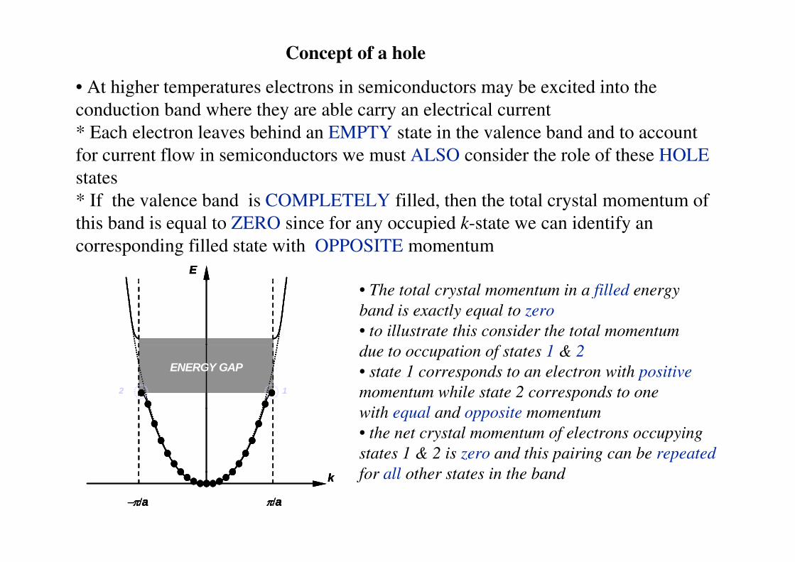
• At higher temperatures electrons in semiconductors may be excited into the
Concept of a hole
At higher temperatures electrons in semiconductors may be excited into the conduction band where they are able carry an electrical current * Each electron leaves behind an EMPTY state in the valence band and to account for current flow in semiconductors we must ALSO consider the role of these HOLEfor current flow in semiconductors we must ALSO consider the role of these HOLEstates* If the valence band is COMPLETELY filled, then the total crystal momentum of hi b d i l ZERO i f i d k id if this band is equal to ZERO since for any occupied k-state we can identify an
corresponding filled state with OPPOSITE momentum EEE
• The total crystal momentum in a filled energyband is exactly equal to zero• to illustrate this consider the total momentumd
ENERGY GAPENERGY GAPENERGY GAP
12
due to occupation of states 1 & 2• state 1 corresponds to an electron with positivemomentum while state 2 corresponds to one
ith l d it twith equal and opposite momentum• the net crystal momentum of electrons occupyingstates 1 & 2 is zero and this pairing can be repeatedfor all other states in the bandk
π/a−π/a
k
π/a−π/a
k
π/a−π/a
for all other states in the band
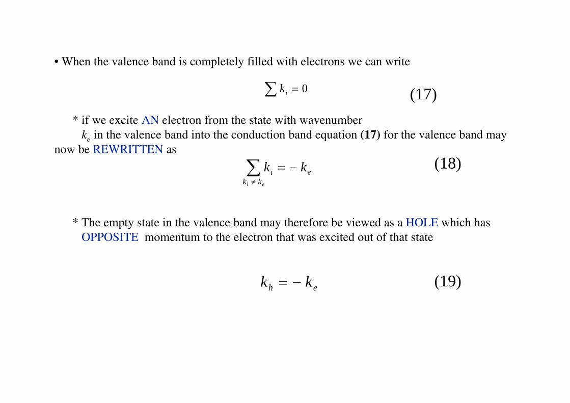
• When the valence band is completely filled with electrons we can writeWhen the valence band is completely filled with electrons we can write
0=∑ ik (17)* if we excite AN electron from the state with wavenumber
ke in the valence band into the conduction band equation (17) for the valence band may now be REWRITTEN as
ekk
i kkei
−=∑≠
(18)
* The empty state in the valence band may therefore be viewed as a HOLE which has OPPOSITE momentum to the electron that was excited out of that state
eh kk −= (19)
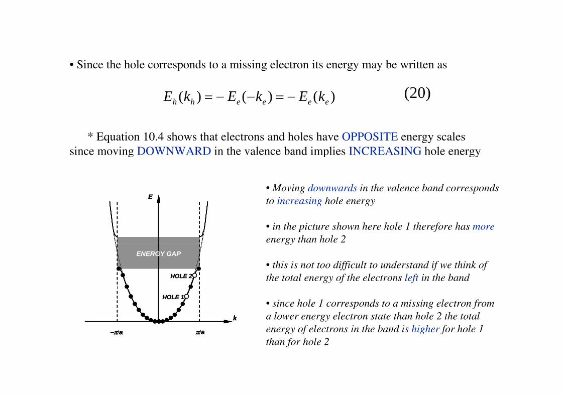
• Since the hole corresponds to a missing electron its energy may be written as• Since the hole corresponds to a missing electron its energy may be written as
)()()( eeeehh kEkEkE −=−−= (20)
* Equation 10.4 shows that electrons and holes have OPPOSITE energy scales since moving DOWNWARD in the valence band implies INCREASING hole energy since moving DOWNWARD in the valence band implies INCREASING hole energy
EEE• Moving downwards in the valence band correspondst i i h l EEE to increasing hole energy
• in the picture shown here hole 1 therefore has moreenergy than hole 2
ENERGY GAP
HOLE 2
ENERGY GAPENERGY GAP
HOLE 2
gy
• this is not too difficult to understand if we think ofthe total energy of the electrons left in the band
k
π/a−π/a
HOLE 1
k
π/a−π/a
k
π/a−π/a
HOLE 1• since hole 1 corresponds to a missing electron froma lower energy electron state than hole 2 the totalenergy of electrons in the band is higher for hole 1π/aπ/a π/aπ/a π/aπ/a gy f g fthan for hole 2
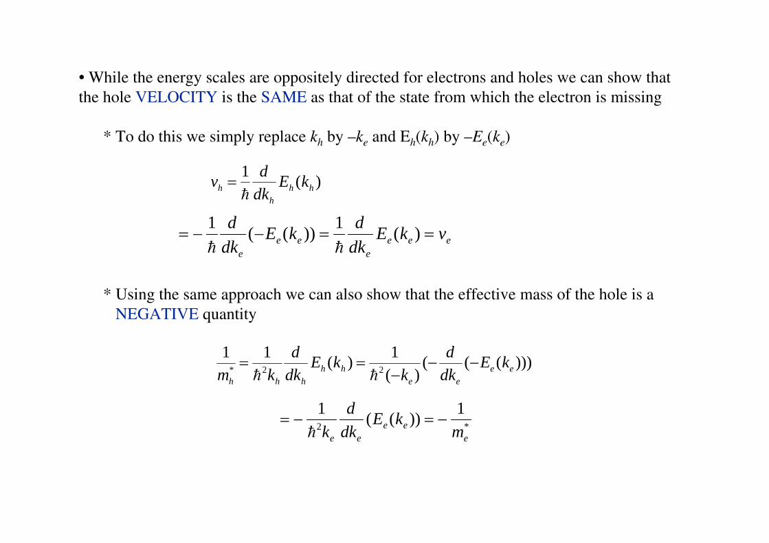
• While the energy scales are oppositely directed for electrons and holes we can show that the hole VELOCITY is the SAME as that of the state from which the electron is missing
* To do this we simply replace kh by –ke and Eh(kh) by –Ee(ke)
)(1hh
hh kE
dkdv =
eeee
eee
vkEdkdkE
dkd
==−−= )(1))((1
* Using the same approach we can also show that the effective mass of the hole is a NEGATIVE quantity
)))((()(
1)(1122* ee
eehh
hhh
kEdkd
kkE
dkd
km−−
−==
*21))((1
eee
ee mkE
dkd
k−=−=
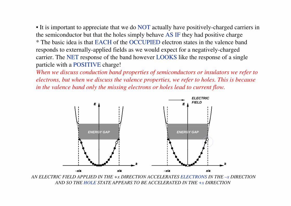
• It is important to appreciate that we do NOT actually have positively-charged carriers in h i d b h h h l i l b h AS IF h h d i i hthe semiconductor but that the holes simply behave AS IF they had positive charge
* The basic idea is that EACH of the OCCUPIED electron states in the valence band responds to externally-applied fields as we would expect for a negatively-charged
rri r Th NET r p n f th b nd h r LOOKS lik th r p n f in l carrier. The NET response of the band however LOOKS like the response of a single particle with a POSITIVE charge! When we discuss conduction band properties of semiconductors or insulators we refer to electrons but when we discuss the valence properties we refer to holes This is because electrons, but when we discuss the valence properties, we refer to holes. This is because in the valence band only the missing electrons or holes lead to current flow.
ELECTRICFIELDE EEEE EE FIELDE EEEE EE
ENERGY GAP ENERGY GAPENERGY GAPENERGY GAPENERGY GAP ENERGY GAPENERGY GAP
k
π/a−π/a
k
π/a−π/a
k
π/a−π/a
k
π/a−π/a
k
π/a−π/a
k
π/a−π/a
k
π/a−π/a
AN ELECTRIC FIELD APPLIED IN THE +x DIRECTION ACCELERATES ELECTRONS IN THE –x DIRECTIONAND SO THE HOLE STATE APPEARS TO BE ACCELERATED IN THE +x DIRECTION
General commentsGeneral commentsThermal vibrations or energy can be used to create a
hole by exciting an electron from the valence band to thehole by exciting an electron from the valence band to theconduction band
I i t i i ( d d) i d t thIn an intrinsic (undoped) semiconductor, the
number of holes in the valence band equals the electronsin the conduction band
Holes can move about the valence band andrecombine with electrons in the conduction band (todisappear)
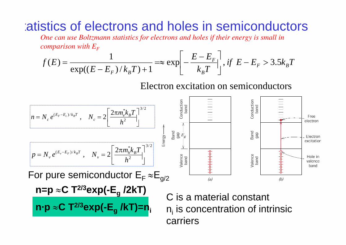
tatistics of electrons and holes in semiconductors One can use Boltzmann statistics for electrons and holes if their energy is small in
TkEEifTkEE
TkEEEf BF
F 5.3,exp1)/)((
1)( >−⎥⎦
⎤⎢⎣
⎡ −−=≈=
One can use Boltzmann statistics for electrons and holes if their energy is small in comparison with EF
TkTkEE BFBBF 1)/)exp(( ⎥
⎦⎢⎣+−
Electron excitation on semiconductors
2/3
2
*/)( 22, ⎥
⎦
⎤⎢⎣
⎡ π== −
hTkmNeNn Be
cTkEE
cBcF
⎦⎣ h
2/3*2 ⎤⎡ π Tkm2
/)( 22, ⎥⎦
⎤⎢⎣
⎡ π== −
hTkmNeNp Bh
vTkEE
vBFv
For pure semiconductor EF ≈Eg/2
n=p ≈C T2/3exp(-Eg /2kT)C is a material constant
i t ti f i t i i
For pure semiconductor EF Eg/2
n p C T2/3exp( E /kT)=n ni is concentration of intrinsic carriers
n·p ≈C T2/3exp(-Eg /kT)=ni
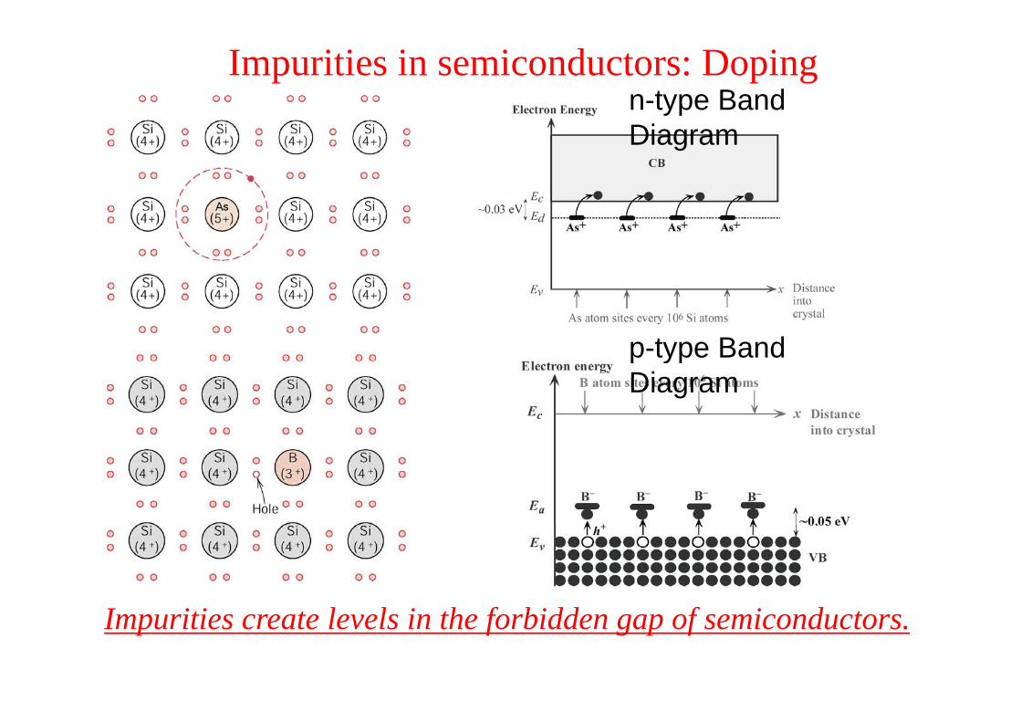
Impurities in semiconductors: Dopingn-type Band ypDiagram
p-type Band p ypDiagram
Impurities create levels in the forbidden gap of semiconductors.
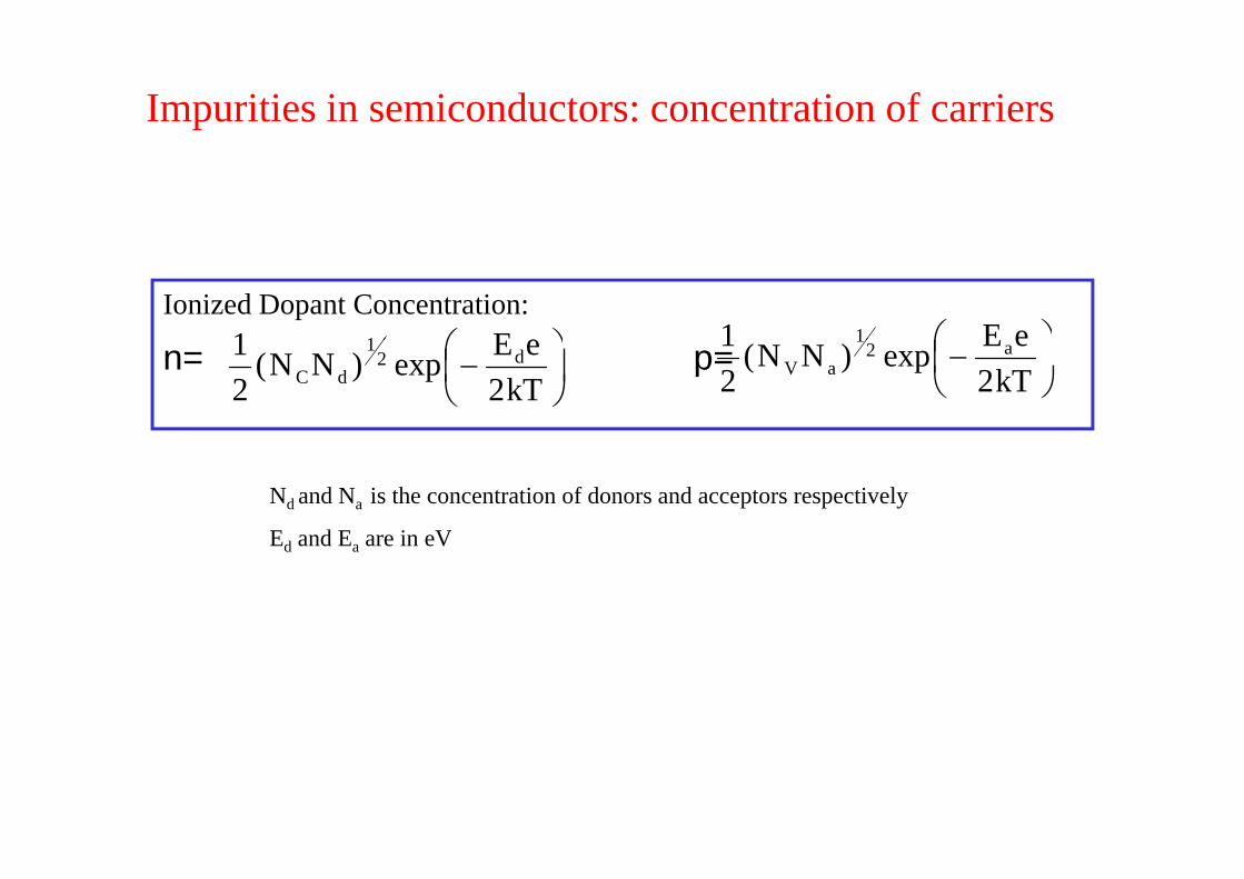
Impurities in semiconductors: concentration of carriers
Ionized Dopant Concentration:⎞⎛ eE1 1 ⎟
⎞⎜⎛ eE1 1
n= p=⎟⎠⎞
⎜⎝⎛ −
kT2eEexp)NN(
21 d2
1
dC⎟⎠⎞
⎜⎝⎛ −
kT2eEexp)NN(
21 a2
1
aV
Nd and Na is the concentration of donors and acceptors respectively
E and E are in eVEd and Ea are in eV
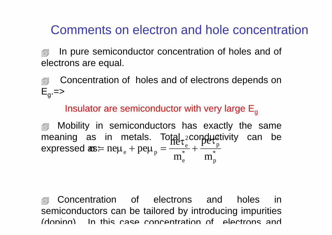
Comments on electron and hole concentrationIn pure semiconductor concentration of holes and of
electrons are equalelectrons are equal.
Concentration of holes and of electrons depends onE =>Eg.=>
Insulator are semiconductor with very large Eg
Mobility in semiconductors has exactly the samemeaning as in metals. Total conductivity can be2
p2 pene ττ
expressed as: *p
p*e
epe m
pm
nepene +τ
=μ+μ=σ
C t ti f l t d h l iConcentration of electrons and holes insemiconductors can be tailored by introducing impurities(doping) In this case concentration of electrons and
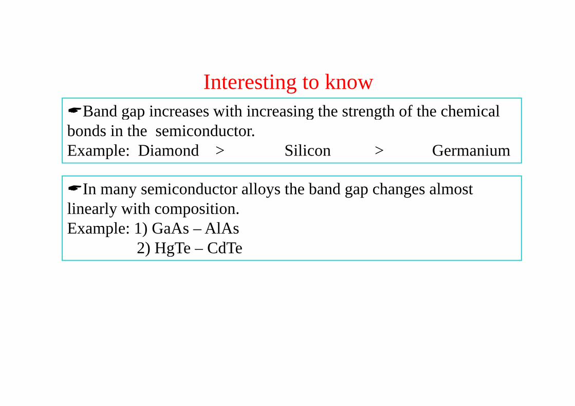
Interesting to knowBand gap increases with increasing the strength of the chemicalBand gap increases with increasing the strength of the chemical
bonds in the semiconductor.Example: Diamond > Silicon > Germaniump
In many semiconductor alloys the band gap changes almost li l i h i ilinearly with composition.Example: 1) GaAs – AlAs
2) HgTe – CdTe2) HgTe – CdTe
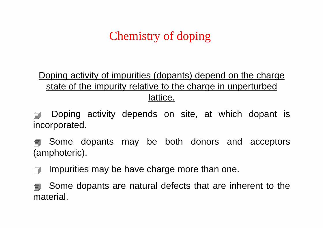
Chemistry of dopingChemistry of doping
Doping activity of impurities (dopants) depend on the charge state of the impurity relative to the charge in unperturbedstate of the impurity relative to the charge in unperturbed
lattice.
Doping activity depends on site at which dopant isDoping activity depends on site, at which dopant isincorporated.
Some dopants may be both donors and acceptorsSome dopants may be both donors and acceptors(amphoteric).
I iti b h h thImpurities may be have charge more than one.
Some dopants are natural defects that are inherent to thematerial.
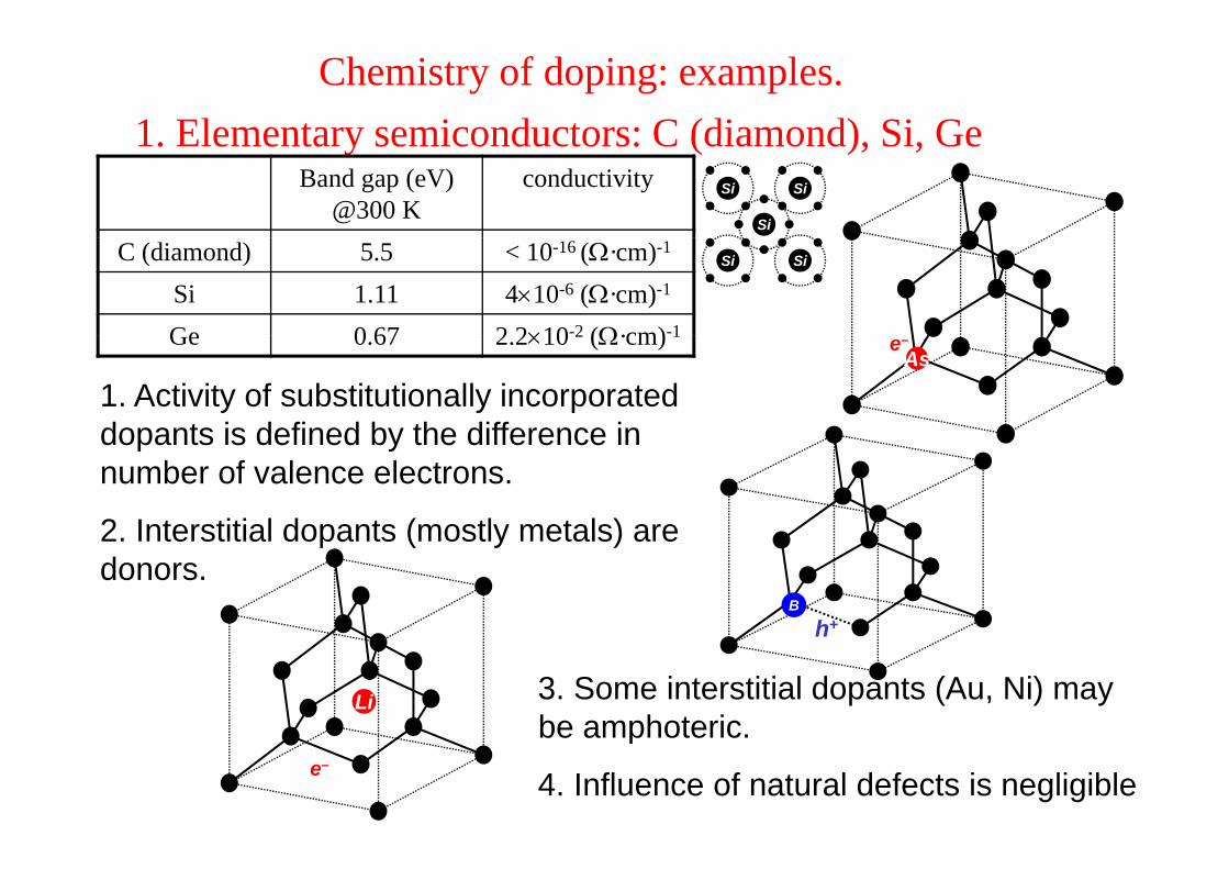
Chemistry of doping: examples. 1 Elementary semiconductors: C (diamond) Si Ge1. Elementary semiconductors: C (diamond), Si, Ge
conductivityBand gap (eV) @300 K
Si
Si Si
< 10-16 (Ω·cm)-15.5C (diamond)4×10⁻⁶ (Ω·cm)-11.11Si
2 2×10⁻² (Ω·cm)-10 67Ge
SiSi
2.2×10 2 (Ω·cm) 10.67Ge
1. Activity of substitutionally incorporated dopants is defined by the difference in
e–As
dopants is defined by the difference in number of valence electrons.
2 Interstitial dopants (mostly metals) are2. Interstitial dopants (mostly metals) are donors.
B
h+h
Li 3. Some interstitial dopants (Au, Ni) may be amphoteric
e–
be amphoteric.
4. Influence of natural defects is negligible.
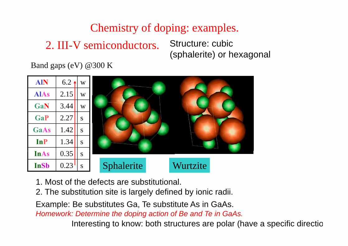
Chemistry of doping: examples. 2. III-V semiconductors. Structure: cubic
(sphalerite) or hexagonalBand gaps (eV) @300 K
w6.2AlN w2 15AlAs
Band gaps (eV) @300 K
w2.15AlAsw3.44GaNs2.27GaPs1.42GaAss1.34InP
Wurtzites0.35InAss0.23InSb Sphalerite
1 M f h d f b i i l1. Most of the defects are substitutional. 2. The substitution site is largely defined by ionic radii.Example: Be substitutes Ga, Te substitute As in GaAs.Example: Be substitutes Ga, Te substitute As in GaAs. Homework: Determine the doping action of Be and Te in GaAs.
Interesting to know: both structures are polar (have a specific directio
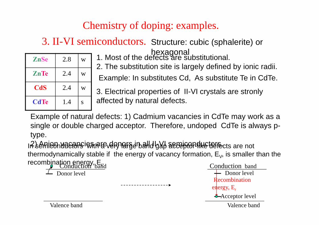
Chemistry of doping: examples. 3. II-VI semiconductors.
w2.8ZnSe
Structure: cubic (sphalerite) or hexagonal
1. Most of the defects are substitutional. w2.8ZnSe
w2.4ZnTe
w2 4CdS
2. The substitution site is largely defined by ionic radii.Example: In substitutes Cd, As substitute Te in CdTe.
w2.4CdS
s1.4CdTe3. Electrical properties of II-VI crystals are stronly affected by natural defects.
Example of natural defects: 1) Cadmium vacancies in CdTe may work as a single or double charged acceptor. Therefore, undoped CdTe is always p-type. yp2) Anion vacancies are donors in all II-VI semiconductors.In semiconductors with a very large band gap acceptor-like defects are not
thermodynamically stable if the energy of vacancy formation, EV, is smaller than the recombination energy EC d i C d irecombination energy, Er.
Donor levelConduction band Conduction band
Recombination energy, Er
Donor level
Valence bandAcceptor level
Valence band
energy, Er