SLLIMM -nano 2nd series IPM, 3-phase inverter, 3 A, 1.6 … V T j Power chip operating junction...
25
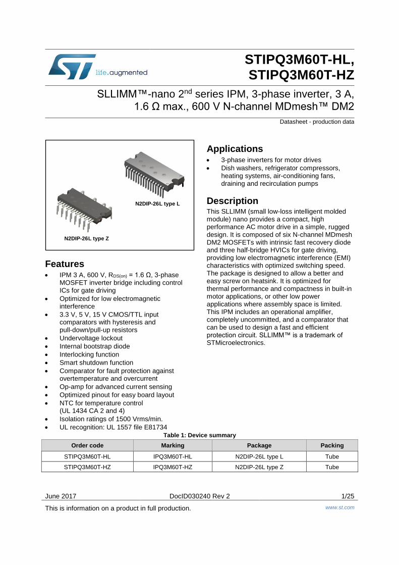
June 2017 DocID030240 Rev 2 1/25 This is information on a product in full production. www.st.com STIPQ3M60T-HL, STIPQ3M60T-HZ SLLIMM™-nano 2 nd series IPM, 3-phase inverter, 3 A, 1.6 Ω max., 600 V N-channel MDmesh™ DM2 Datasheet - production data Features IPM 3 A, 600 V, RDS(on) = 1.6 Ω, 3-phase MOSFET inverter bridge including control ICs for gate driving Optimized for low electromagnetic interference 3.3 V, 5 V, 15 V CMOS/TTL input comparators with hysteresis and pull-down/pull-up resistors Undervoltage lockout Internal bootstrap diode Interlocking function Smart shutdown function Comparator for fault protection against overtemperature and overcurrent Op-amp for advanced current sensing Optimized pinout for easy board layout NTC for temperature control (UL 1434 CA 2 and 4) Isolation ratings of 1500 Vrms/min. UL recognition: UL 1557 file E81734 Applications 3-phase inverters for motor drives Dish washers, refrigerator compressors, heating systems, air-conditioning fans, draining and recirculation pumps Description This SLLIMM (small low-loss intelligent molded module) nano provides a compact, high performance AC motor drive in a simple, rugged design. It is composed of six N-channel MDmesh DM2 MOSFETs with intrinsic fast recovery diode and three half-bridge HVICs for gate driving, providing low electromagnetic interference (EMI) characteristics with optimized switching speed. The package is designed to allow a better and easy screw on heatsink. It is optimized for thermal performance and compactness in built-in motor applications, or other low power applications where assembly space is limited. This IPM includes an operational amplifier, completely uncommitted, and a comparator that can be used to design a fast and efficient protection circuit. SLLIMM™ is a trademark of STMicroelectronics. Table 1: Device summary Order code Marking Package Packing STIPQ3M60T-HL IPQ3M60T-HL N2DIP-26L type L Tube STIPQ3M60T-HZ IPQ3M60T-HZ N2DIP-26L type Z Tube N2DIP-26L type L N2DIP-26L type Z
Transcript of SLLIMM -nano 2nd series IPM, 3-phase inverter, 3 A, 1.6 … V T j Power chip operating junction...
June 2017 DocID030240 Rev 2 1/25
This is information on a product in full production. www.st.com
STIPQ3M60T-HL, STIPQ3M60T-HZ
SLLIMM™-nano 2nd series IPM, 3-phase inverter, 3 A, 1.6 Ω max., 600 V N-channel MDmesh™ DM2
Datasheet - production data
Features IPM 3 A, 600 V, RDS(on) = 1.6 Ω, 3-phase
MOSFET inverter bridge including control ICs for gate driving
Optimized for low electromagnetic interference
3.3 V, 5 V, 15 V CMOS/TTL input comparators with hysteresis and pull-down/pull-up resistors
Undervoltage lockout
Internal bootstrap diode
Interlocking function
Smart shutdown function
Comparator for fault protection against overtemperature and overcurrent
Op-amp for advanced current sensing
Optimized pinout for easy board layout
NTC for temperature control (UL 1434 CA 2 and 4)
Isolation ratings of 1500 Vrms/min.
UL recognition: UL 1557 file E81734
Applications 3-phase inverters for motor drives
Dish washers, refrigerator compressors, heating systems, air-conditioning fans, draining and recirculation pumps
Description This SLLIMM (small low-loss intelligent molded module) nano provides a compact, high performance AC motor drive in a simple, rugged design. It is composed of six N-channel MDmesh DM2 MOSFETs with intrinsic fast recovery diode and three half-bridge HVICs for gate driving, providing low electromagnetic interference (EMI) characteristics with optimized switching speed. The package is designed to allow a better and easy screw on heatsink. It is optimized for thermal performance and compactness in built-in motor applications, or other low power applications where assembly space is limited. This IPM includes an operational amplifier, completely uncommitted, and a comparator that can be used to design a fast and efficient protection circuit. SLLIMM™ is a trademark of STMicroelectronics.
Table 1: Device summary
Order code Marking Package Packing
STIPQ3M60T-HL IPQ3M60T-HL N2DIP-26L type L Tube
STIPQ3M60T-HZ IPQ3M60T-HZ N2DIP-26L type Z Tube
N2DIP-26L type L
N2DIP-26L type Z
Contents STIPQ3M60T-HL, STIPQ3M60T-HZ
2/25 DocID030240 Rev 2
Contents
1 Internal schematic diagram and pin configuration ....................... 3
2 Electrical ratings ............................................................................. 5
2.1 Absolute maximum ratings ................................................................ 5
2.2 Thermal data ..................................................................................... 5
3 Electrical characteristics ................................................................ 6
3.1 Inverter part ....................................................................................... 6
3.2 Control part ....................................................................................... 8
3.2.1 NTC thermistor ................................................................................. 10
3.3 Waveform definitions ....................................................................... 13
4 Smart shutdown function ............................................................. 14
5 Application circuit example .......................................................... 16
5.1 Guidelines ....................................................................................... 17
6 Package information ..................................................................... 19
6.1 N2DIP-26L type L package information .......................................... 19
6.2 N2DIP-26L type Z package information .......................................... 21
6.3 N2DIP-26L packing information ...................................................... 23
7 Revision history ............................................................................ 24
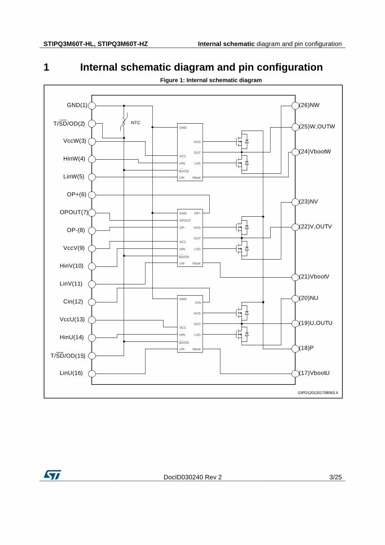
STIPQ3M60T-HL, STIPQ3M60T-HZ Internal schematic diagram and pin configuration
DocID030240 Rev 2 3/25
1 Internal schematic diagram and pin configuration Figure 1: Internal schematic diagram
NTC
GND(1)
T/SD/OD(2)
VccW(3)
HinW(4)
LinW(5)
OP+(6)
OPOUT(7)
OP-(8)
VccV(9)
HinV(10)
LinV(11)
Cin(12)
VccU(13)
HinU(14)
T/SD/OD(15)
LinU(16) (17)VbootU
(18)P
(19)U,OUTU
(20)NU
(21)VbootV
(22)V,OUTV
(23)NV
(24)VbootW
(25)W,OUTW
(26)NW
GND
LIN
VCC
HVG
CIN
SD/OD
OUT
LVG
Vboot
HIN
GND
OPOUT
LIN
VCC
HVG
OP+
OP-
SD/OD
OUT
LVG
Vboot
HIN
GND
LIN
VCC
HVG
SD/OD
OUT
LVG
Vboot
HIN
GIPD120120170806S A
Internal schematic diagram and pin configuration STIPQ3M60T-HL, STIPQ3M60T-HZ
4/25 DocID030240 Rev 2
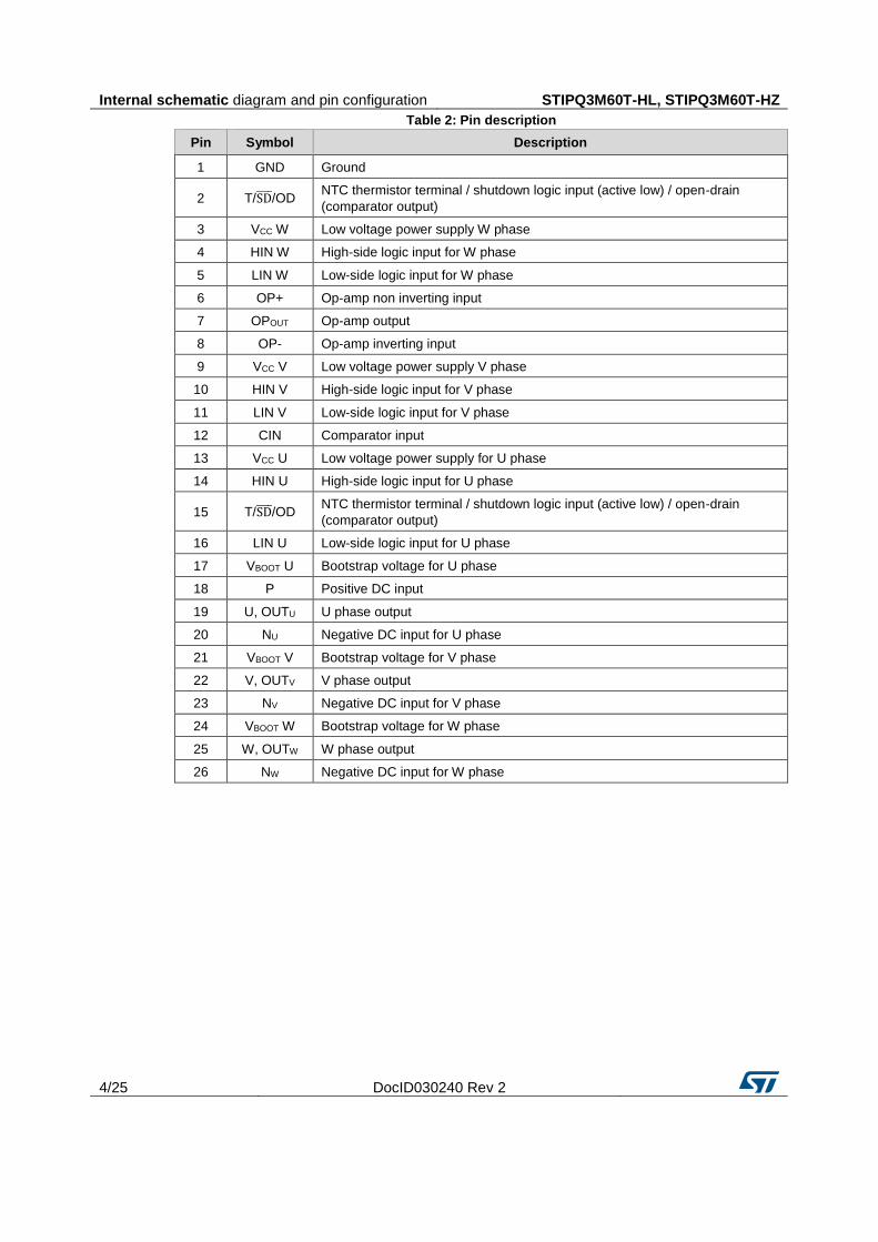
Table 2: Pin description
Pin Symbol Description
1 GND Ground
2 T/SD /OD NTC thermistor terminal / shutdown logic input (active low) / open-drain
(comparator output)
3 VCC W Low voltage power supply W phase
4 HIN W High-side logic input for W phase
5 LIN W Low-side logic input for W phase
6 OP+ Op-amp non inverting input
7 OPOUT Op-amp output
8 OP- Op-amp inverting input
9 VCC V Low voltage power supply V phase
10 HIN V High-side logic input for V phase
11 LIN V Low-side logic input for V phase
12 CIN Comparator input
13 VCC U Low voltage power supply for U phase
14 HIN U High-side logic input for U phase
15 T/SD /OD NTC thermistor terminal / shutdown logic input (active low) / open-drain
(comparator output)
16 LIN U Low-side logic input for U phase
17 VBOOT U Bootstrap voltage for U phase
18 P Positive DC input
19 U, OUTU U phase output
20 NU Negative DC input for U phase
21 VBOOT V Bootstrap voltage for V phase
22 V, OUTV V phase output
23 NV Negative DC input for V phase
24 VBOOT W Bootstrap voltage for W phase
25 W, OUTW W phase output
26 NW Negative DC input for W phase
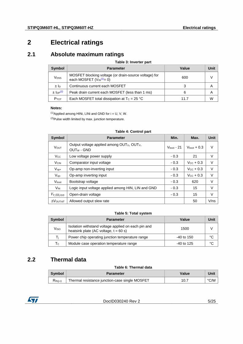
STIPQ3M60T-HL, STIPQ3M60T-HZ Electrical ratings
DocID030240 Rev 2 5/25
2 Electrical ratings
2.1 Absolute maximum ratings
Table 3: Inverter part
Symbol Parameter Value Unit
VDSS MOSFET blocking voltage (or drain-source voltage) for
each MOSFET (VIN(1)= 0)
600 V
± ID Continuous current each MOSFET 3 A
± IDP(2) Peak drain current each MOSFET (less than 1 ms) 6 A
PTOT Each MOSFET total dissipation at TC = 25 °C 11.7 W
Notes:
(1)Applied among HINi, LINi and GND for i = U, V, W. (2)Pulse width limited by max. junction temperature.
Table 4: Control part
Symbol Parameter Min. Max. Unit
VOUT Output voltage applied among OUTU, OUTV,
OUTW - GND Vboot - 21 Vboot + 0.3 V
VCC Low voltage power supply - 0.3 21 V
VCIN Comparator input voltage - 0.3 VCC + 0.3 V
Vop+ Op-amp non-inverting input - 0.3 VCC + 0.3 V
Vop- Op-amp inverting input - 0.3 VCC + 0.3 V
Vboot Bootstrap voltage - 0.3 620 V
VIN Logic input voltage applied among HIN, LIN and GND - 0.3 15 V
𝑉𝑇/𝑆𝐷 /𝑂𝐷 Open-drain voltage - 0.3 15 V
∆VOUT/dT Allowed output slew rate
50 V/ns
Table 5: Total system
Symbol Parameter Value Unit
VISO Isolation withstand voltage applied on each pin and
heatsink plate (AC voltage, t = 60 s) 1500 V
Tj Power chip operating junction temperature range -40 to 150 °C
TC Module case operation temperature range -40 to 125 °C
2.2 Thermal data
Table 6: Thermal data
Symbol Parameter Value Unit
Rth(j-c) Thermal resistance junction-case single MOSFET 10.7 °C/W
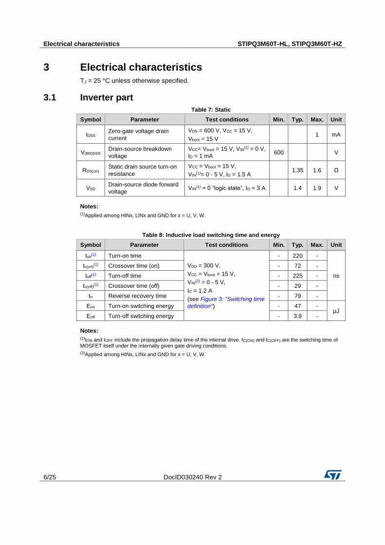
Electrical characteristics STIPQ3M60T-HL, STIPQ3M60T-HZ
6/25 DocID030240 Rev 2
3 Electrical characteristics
TJ = 25 °C unless otherwise specified.
3.1 Inverter part
Table 7: Static
Symbol Parameter Test conditions Min. Typ. Max. Unit
IDSS Zero-gate voltage drain
current
VDS = 600 V, VCC = 15 V,
Vboot = 15 V 1 mA
V(BR)DSS Drain-source breakdown
voltage
VCC= Vboot = 15 V, VIN(1) = 0 V,
ID = 1 mA 600
V
RDS(on) Static drain source turn-on
resistance
VCC = Vboot = 15 V,
VIN(1)= 0 - 5 V, ID = 1.5 A
1.35 1.6 Ω
VSD Drain-source diode forward
voltage VIN
(1) = 0 “logic state”, ID = 3 A
1.4 1.9 V
Notes:
(1)Applied among HINx, LINx and GND for x = U, V, W.
Table 8: Inductive load switching time and energy
Symbol Parameter Test conditions Min. Typ. Max. Unit
ton(1) Turn-on time
VDD = 300 V,
VCC = Vboot = 15 V,
VIN(2) = 0 - 5 V,
IC = 1.2 A
(see Figure 3: "Switching time
definition")
- 220 -
ns
tc(on)(1) Crossover time (on) - 72 -
toff(1) Turn-off time - 225 -
tc(off)(1) Crossover time (off) - 29 -
trr Reverse recovery time - 79 -
Eon Turn-on switching energy - 47 - µJ
Eoff Turn-off switching energy - 3.9 -
Notes:
(1)tON and tOFF include the propagation delay time of the internal drive. tC(ON) and tC(OFF) are the switching time of MOSFET itself under the internally given gate driving conditions. (2)Applied among HINx, LINx and GND for x = U, V, W.
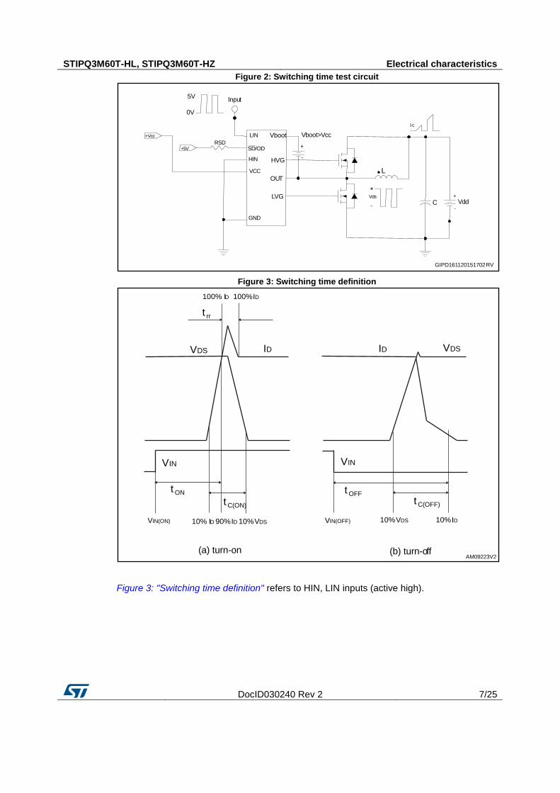
STIPQ3M60T-HL, STIPQ3M60T-HZ Electrical characteristics
DocID030240 Rev 2 7/25
Figure 2: Switching time test circuit
Figure 3: Switching time definition
Figure 3: "Switching time definition" refers to HIN, LIN inputs (active high).
+5V
+Vcc
Input
VddC
L
Vboot>Vcc
5V
0V
+
-
Vds
Ic
+
-
RSD
GND
LIN
VCC
LVG
SD/OD
OUT
HVG
Vboot
HIN
+
-
GIPD161120151702RV
VDS ID ID
VIN
t ON
t C(ON)
VIN(ON) 10% ID 90%ID 10%VDS
(a) turn-on (b) turn-off
t rr
100% ID 100%ID
VIN
VDS
t OFF
t C(OFF)
VIN(OFF) 10%VDS 10%ID
AM09223V2
Electrical characteristics STIPQ3M60T-HL, STIPQ3M60T-HZ
8/25 DocID030240 Rev 2
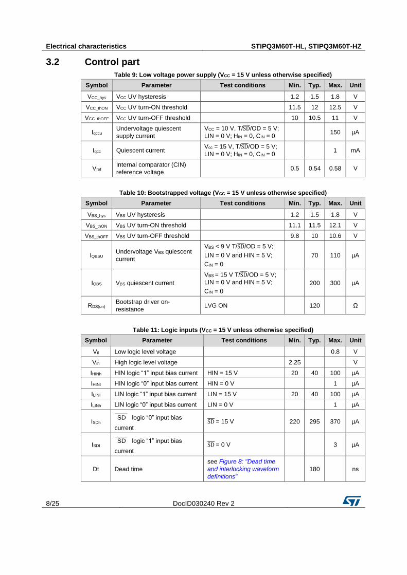
3.2 Control part
Table 9: Low voltage power supply (VCC = 15 V unless otherwise specified)
Symbol Parameter Test conditions Min. Typ. Max. Unit
VCC_hys VCC UV hysteresis
1.2 1.5 1.8 V
VCC_thON VCC UV turn-ON threshold
11.5 12 12.5 V
VCC_thOFF VCC UV turn-OFF threshold
10 10.5 11 V
Iqccu Undervoltage quiescent
supply current
VCC = 10 V, T/SD /OD = 5 V;
LIN = 0 V; HIN = 0, CIN = 0 150 µA
Iqcc Quiescent current Vcc = 15 V, T/SD /OD = 5 V;
LIN = 0 V; HIN = 0, CIN = 0 1 mA
Vref Internal comparator (CIN)
reference voltage 0.5 0.54 0.58 V
Table 10: Bootstrapped voltage (VCC = 15 V unless otherwise specified)
Symbol Parameter Test conditions Min. Typ. Max. Unit
VBS_hys VBS UV hysteresis
1.2 1.5 1.8 V
VBS_thON VBS UV turn-ON threshold
11.1 11.5 12.1 V
VBS_thOFF VBS UV turn-OFF threshold
9.8 10 10.6 V
IQBSU Undervoltage VBS quiescent
current
VBS < 9 V T/SD /OD = 5 V;
LIN = 0 V and HIN = 5 V;
CIN = 0
70 110 µA
IQBS VBS quiescent current
VBS = 15 V T/SD /OD = 5 V;
LIN = 0 V and HIN = 5 V;
CIN = 0
200 300 µA
RDS(on) Bootstrap driver on-
resistance LVG ON
120
Ω
Table 11: Logic inputs (VCC = 15 V unless otherwise specified)
Symbol Parameter Test conditions Min. Typ. Max. Unit
Vil Low logic level voltage
0.8 V
Vih High logic level voltage
2.25
V
IHINh HIN logic “1” input bias current HIN = 15 V 20 40 100 µA
IHINI HIN logic “0” input bias current HIN = 0 V
1 µA
ILINI LIN logic “1” input bias current LIN = 15 V 20 40 100 µA
ILINh LIN logic “0” input bias current LIN = 0 V
1 µA
ISDh SD logic “0” input bias
current SD = 15 V 220 295 370 µA
ISDI SD logic “1” input bias
current SD = 0 V
3 µA
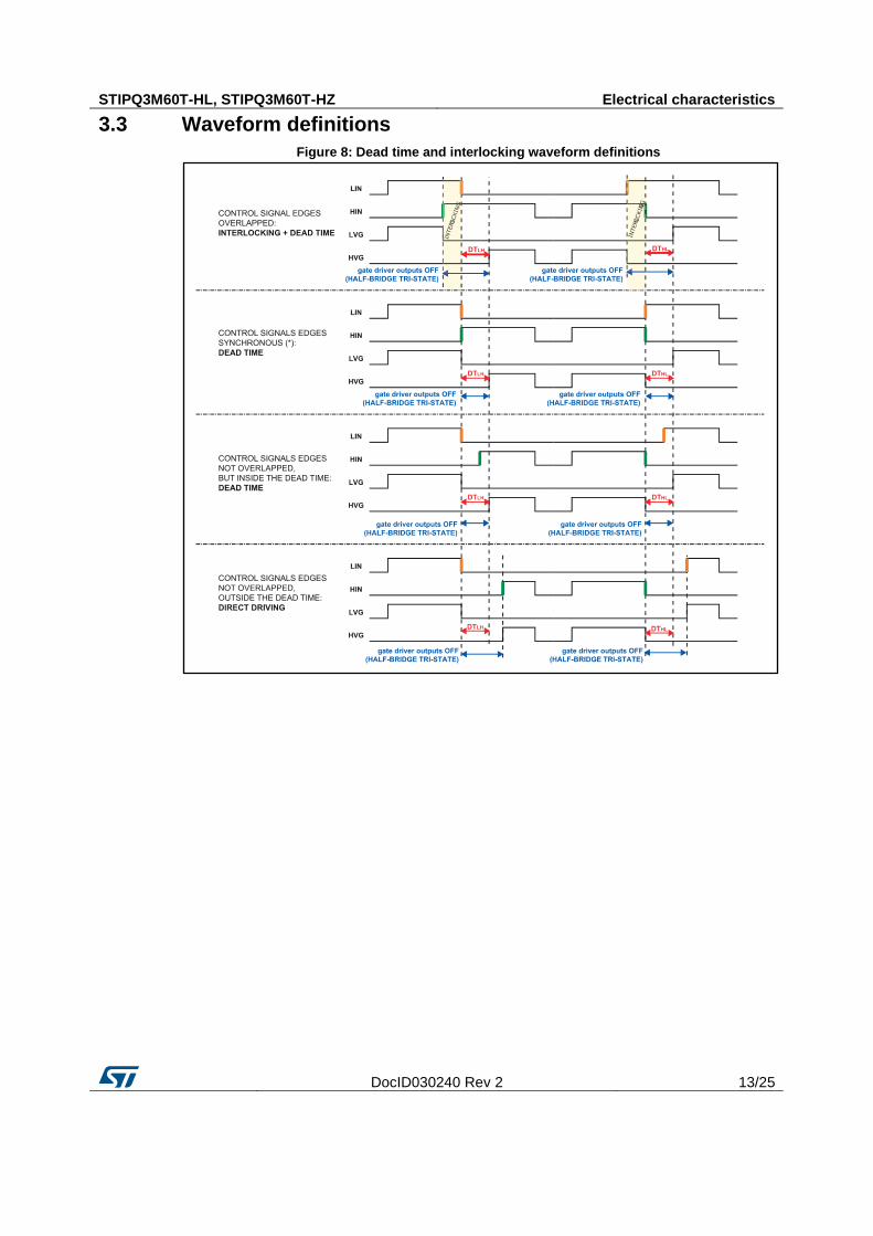
Dt Dead time
see Figure 8: "Dead time
and interlocking waveform
definitions" 180
ns
STIPQ3M60T-HL, STIPQ3M60T-HZ Electrical characteristics
DocID030240 Rev 2 9/25
Table 12: Op-amp characteristics (VCC = 15 V unless otherwise specified)
Symbol Parameter Test conditions Min. Typ. Max. Unit
Vio Input offset voltage Vic = 0 V, Vo = 7.5 V
6 mV
Iio Input offset current Vic = 0 V, Vo = 7.5 V
4 40 nA
Iib Input bias current (1)
100 200 nA
VOL Low level output voltage RL = 10 kΩ to VCC
75 150 mV
VOH High level output voltage RL = 10 kΩ to GND 14 14.7
V
Io Output short-circuit current
Source, Vid = +1 V;
Vo = 0 V 16 30
mA
Sink, Vid = -1 V;
Vo = VCC 50 80
mA
SR Slew rate Vi = 1 - 4 V;
CL = 100 pF; unity gain 2.5 3.8
V/µs
GBWP Gain bandwidth product Vo = 7.5 V 8 12
MHz
Avd Large signal voltage gain RL = 2 kΩ 70 85
dB
SVR Supply voltage rejection ratio vs. VCC 60 75
dB
CMRR Common mode rejection ratio
55 70
dB
Notes:
(1)The direction of the input current is out of the IC.
Table 13: Sense comparator characteristics (VCC = 15 V unless otherwise specified)
Symbol Parameter Test conditions Min. Typ. Max. Unit
Iib Input bias current VCIN = 1 V
3 µA
Vod Open-drain low level output
voltage Iod = 3 mA
0.5 V
RON_OD Open-drain low level output
resistance Iod = 3 mA
166
Ω
RPD_SD SD pull-down resistor (1)
125
kΩ
td_comp Comparator delay T/SD /OD pulled to 5 V
through 100 kΩ resistor 90 130 ns
SR Slew rate CL = 180 pF; Rpu = 5 kΩ
60
V/µs
tsd Shutdown to high / low-side
driver propagation delay
VOUT = 0, Vboot = VCC,
VIN = 0 to 3.3 V 50 125 200
ns
tisd
Comparator triggering to high
/ low-side driver turn-off
propagation delay
Measured applying a
voltage step from 0 V to
3.3 V to pin CIN
50 200 250
Notes:
(1)Equivalent values are as the result of the resistances of three drivers in parallel.
Electrical characteristics STIPQ3M60T-HL, STIPQ3M60T-HZ
10/25 DocID030240 Rev 2
Table 14: Truth table
Conditions Logic input (VI) Output
T/𝐒𝐃 /OD LIN HIN LVG HVG
Shutdown enable half-bridge tri-state L X(1) X(1) L L
Interlocking half-bridge tri-state H H H L L
0 “logic state” half-bridge tri-state H L L L L
1 “logic state” low-side direct driving H H L H L
1 “logic state” high-side direct driving H L H L H
Notes:
(1)X: do not care.
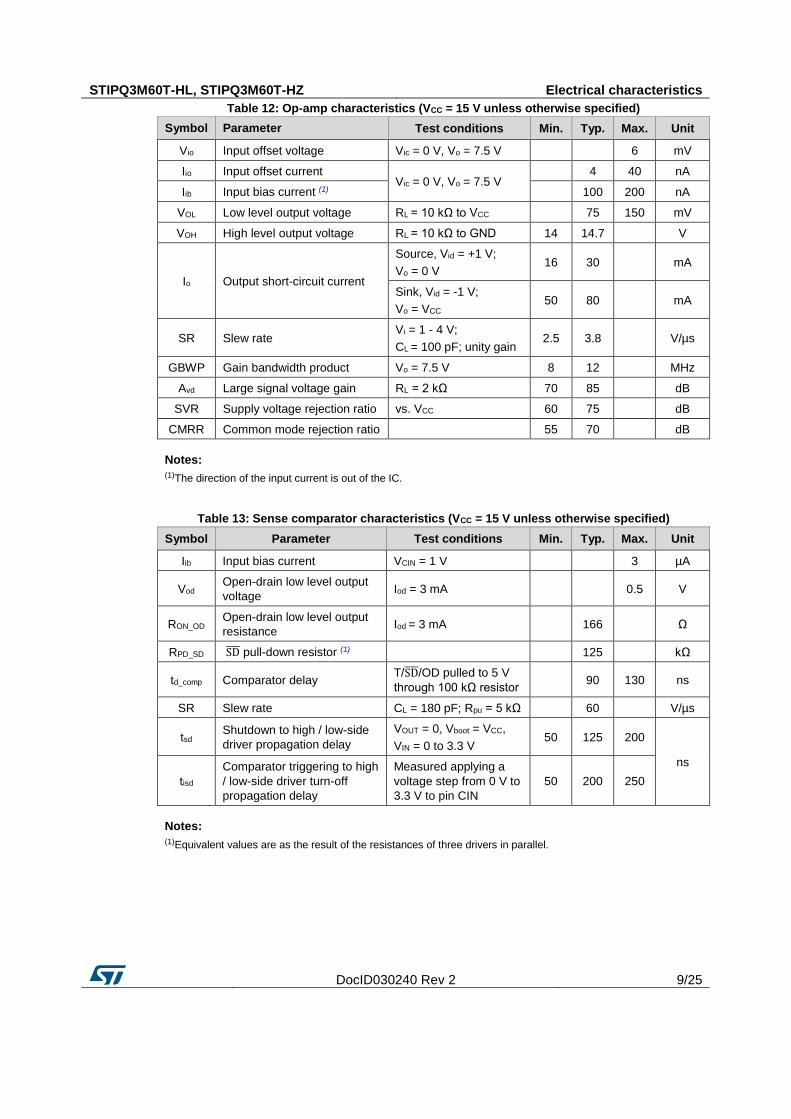
3.2.1 NTC thermistor
Figure 4: Internal structure of 𝐒𝐃 and NTC
RPD_SD: equivalent value as result of resistances of three drivers in parallel.
T/SD/ODV
Vbias
RPD_SD
NTC
LIN
HIN
VCC
GND CIN
LVG
OUT
HVG
Vboot
SD/OD
R SD
C SD
STIPQ3M60T-HL, STIPQ3M60T-HZ Electrical characteristics
DocID030240 Rev 2 11/25
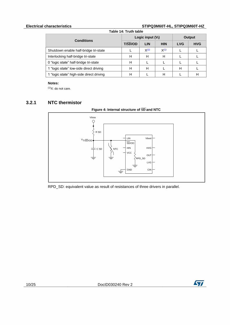
Figure 5: Equivalent resistance (NTC//RPD_SD)
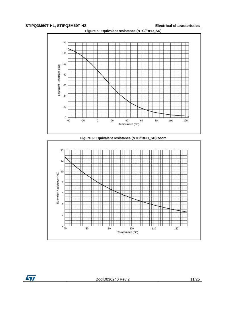
Figure 6: Equivalent resistance (NTC//RPD_SD) zoom
Electrical characteristics STIPQ3M60T-HL, STIPQ3M60T-HZ
12/25 DocID030240 Rev 2
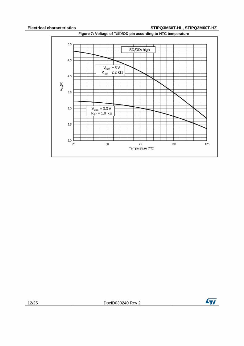
Figure 7: Voltage of T/𝐒𝐃 /OD pin according to NTC temperature
STIPQ3M60T-HL, STIPQ3M60T-HZ Electrical characteristics
DocID030240 Rev 2 13/25
3.3 Waveform definitions
Figure 8: Dead time and interlocking waveform definitions
Smart shutdown function STIPQ3M60T-HL, STIPQ3M60T-HZ
14/25 DocID030240 Rev 2
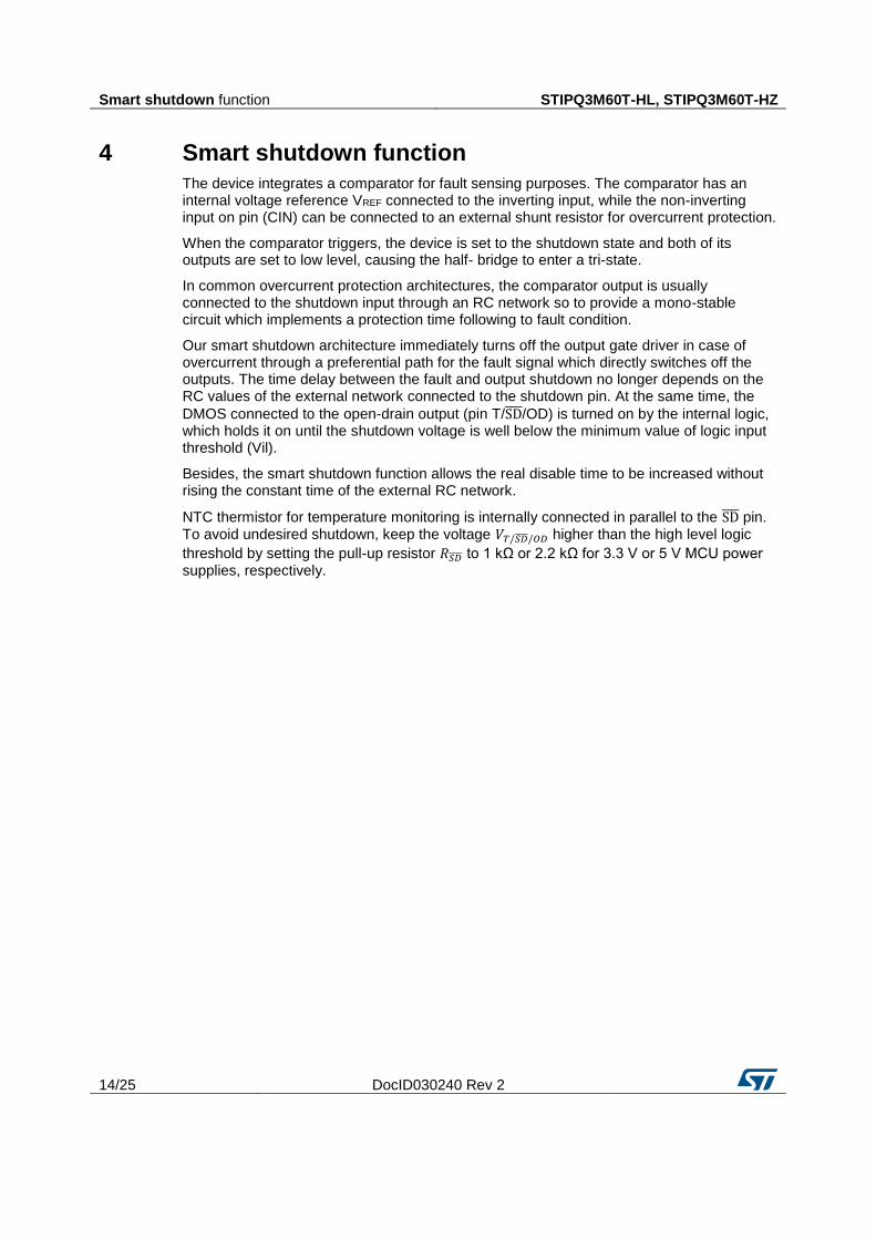
4 Smart shutdown function
The device integrates a comparator for fault sensing purposes. The comparator has an internal voltage reference VREF connected to the inverting input, while the non-inverting input on pin (CIN) can be connected to an external shunt resistor for overcurrent protection.
When the comparator triggers, the device is set to the shutdown state and both of its outputs are set to low level, causing the half- bridge to enter a tri-state.
In common overcurrent protection architectures, the comparator output is usually connected to the shutdown input through an RC network so to provide a mono-stable circuit which implements a protection time following to fault condition.
Our smart shutdown architecture immediately turns off the output gate driver in case of overcurrent through a preferential path for the fault signal which directly switches off the outputs. The time delay between the fault and output shutdown no longer depends on the RC values of the external network connected to the shutdown pin. At the same time, the
DMOS connected to the open-drain output (pin T/SD /OD) is turned on by the internal logic, which holds it on until the shutdown voltage is well below the minimum value of logic input threshold (Vil).
Besides, the smart shutdown function allows the real disable time to be increased without rising the constant time of the external RC network.
NTC thermistor for temperature monitoring is internally connected in parallel to the SD pin. To avoid undesired shutdown, keep the voltage 𝑉𝑇/𝑆𝐷 /𝑂𝐷 higher than the high level logic
threshold by setting the pull-up resistor 𝑅𝑆𝐷 to 1 kΩ or 2.2 kΩ for 3.3 V or 5 V MCU power supplies, respectively.
STIPQ3M60T-HL, STIPQ3M60T-HZ Smart shutdown function
DocID030240 Rev 2 15/25
Figure 9: Smart shutdown timing waveforms
Please refer to Table 13: "Sense comparator characteristics (VCC = 15 V unless otherwise specified)" for internal propagation delay time details.
SHUTDOWN CIRCUIT
An approximation of the disable time is given by:
HIN/LIN
HVG/LVG
open-drain gate(internal)
comp Vref
CP+
PROTECTION
Fast shutdown:
the driver outputs are set to the SD state as soon as the comparatortriggers even if the SD signal hasn’t reached the lowest input threshold
disable time
SD/OD
GIPG080920140931FSR
T/SD/ODV
SMART SD
LOGIC
T/SD/ OD
RPD_SD
C SD
R SD
Vbias
NTC RON_OD
Application circuit example STIPQ3M60T-HL, STIPQ3M60T-HZ
16/25 DocID030240 Rev 2
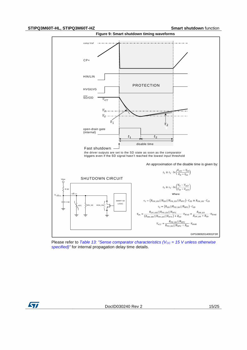
5 Application circuit example Figure 10: Application circuit example
Application designers are free to use a different scheme according to the specifications of the device.
RS
RS
RS
AD
C
M
PW
R_
GN
D
SG
N_G
ND
GN
D(1
)
T/S
D/O
D(1
5)
Hin
W(4
)
VccW
(3)
OP
+(6
)
Lin
W(5
)
VccV
(9)
OP
-(8
)
OP
OU
T(7
)
Cin
(12
)
Lin
V(1
1)
Hin
V(1
0)
Hin
U(1
4)
VccU
(13
)
Lin
U(1
6)
T/S
D/O
D(2
)
(17
)Vb
oo
tU
(18
)P
(19
)U,O
UT
U
(20
)NU
(21
)Vb
oo
tV
(22
)V,O
UT
V
(23
)NV
(24
)Vb
oo
tW
(26
)NW
(25
)W,O
UT
W
R1
R1
R1
R1
R1
R1
R1
R2
R3
R4 R
5
RS
D
RS
F
Rsh
un
t
C1
C1
C1
C1
C1
C1
C3
C3
C3
C4
CS
F
CO
P
CS
D
Cb
oo
tU
Cb
oo
tV
Cb
oo
tW
Cvd
cVD
C
Vc
cD
Z1
DZ
2
DZ
2
DZ
2
5V
/3.3
V
5V
/3.3
V
Cvc
cC
2
GN
D
LIN
VC
C
LV
G
SD
/OD
OU
T
HV
G
Vb
oo
t
HIN
MICROCONTROLLER
Te
mp
.M
on
itorin
g
HIN
U
LIN
U
LIN
V
HIN
V
LIN
W
HIN
W
SD
AD
C
NT
C
+ -
+ -
GN
D
LIN
VC
C
LV
G
CIN
SD
/OD
OU
T
HV
G
Vb
oo
t
HIN
GN
D
OP
OU
T
LIN
VC
C
LV
G
OP
+
OP
-
SD
/OD
OU
T
HV
G
Vb
oo
t
HIN
GADG100620160912FSR
STIPQ3M60T-HL, STIPQ3M60T-HZ Application circuit example
DocID030240 Rev 2 17/25
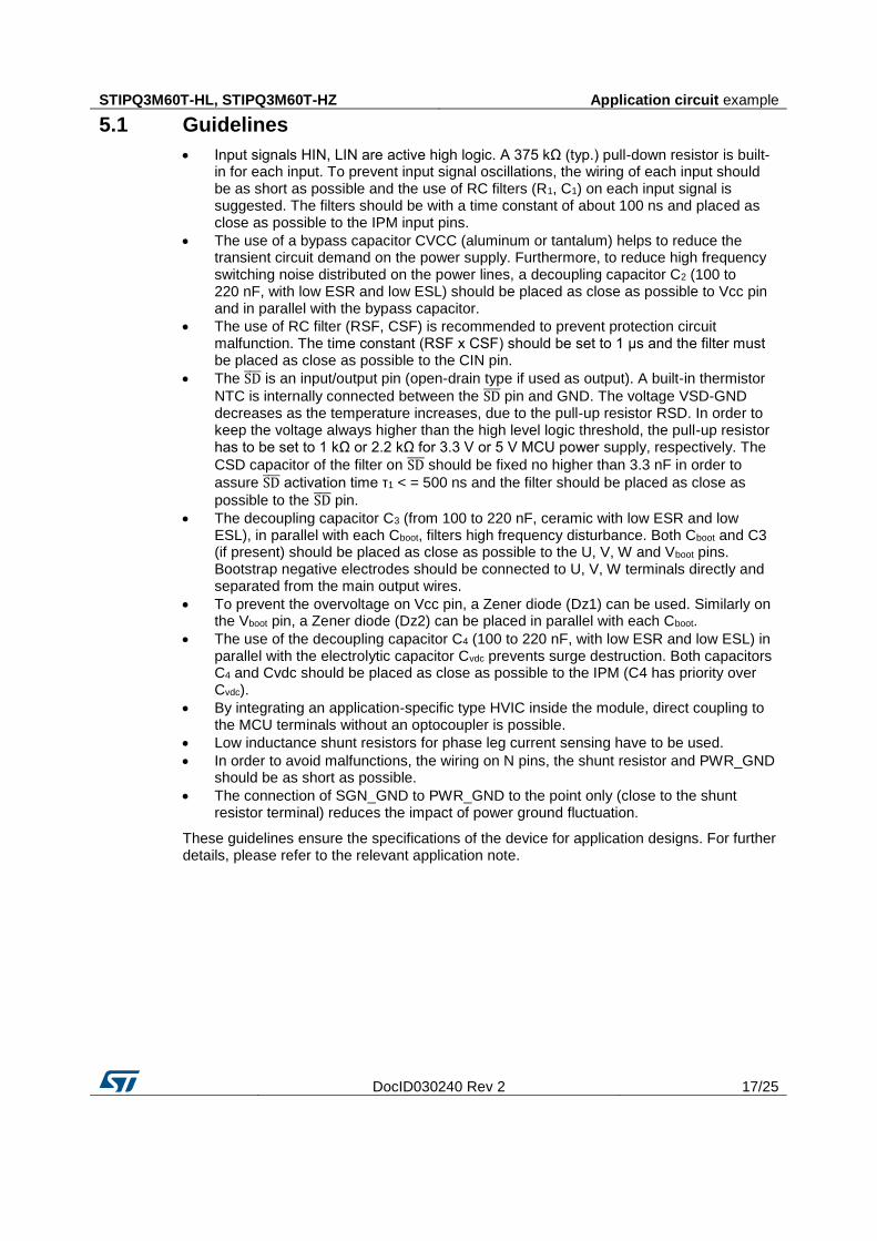
5.1 Guidelines
Input signals HIN, LIN are active high logic. A 375 kΩ (typ.) pull-down resistor is built-in for each input. To prevent input signal oscillations, the wiring of each input should be as short as possible and the use of RC filters (R1, C1) on each input signal is suggested. The filters should be with a time constant of about 100 ns and placed as close as possible to the IPM input pins.
The use of a bypass capacitor CVCC (aluminum or tantalum) helps to reduce the transient circuit demand on the power supply. Furthermore, to reduce high frequency switching noise distributed on the power lines, a decoupling capacitor C2 (100 to 220 nF, with low ESR and low ESL) should be placed as close as possible to Vcc pin and in parallel with the bypass capacitor.
The use of RC filter (RSF, CSF) is recommended to prevent protection circuit malfunction. The time constant (RSF x CSF) should be set to 1 μs and the filter must be placed as close as possible to the CIN pin.
The SD is an input/output pin (open-drain type if used as output). A built-in thermistor
NTC is internally connected between the SD pin and GND. The voltage VSD-GND decreases as the temperature increases, due to the pull-up resistor RSD. In order to keep the voltage always higher than the high level logic threshold, the pull-up resistor has to be set to 1 kΩ or 2.2 kΩ for 3.3 V or 5 V MCU power supply, respectively. The
CSD capacitor of the filter on SD should be fixed no higher than 3.3 nF in order to
assure SD activation time τ1 < = 500 ns and the filter should be placed as close as
possible to the SD pin.
The decoupling capacitor C3 (from 100 to 220 nF, ceramic with low ESR and low ESL), in parallel with each Cboot, filters high frequency disturbance. Both Cboot and C3 (if present) should be placed as close as possible to the U, V, W and Vboot pins. Bootstrap negative electrodes should be connected to U, V, W terminals directly and separated from the main output wires.
To prevent the overvoltage on Vcc pin, a Zener diode (Dz1) can be used. Similarly on the Vboot pin, a Zener diode (Dz2) can be placed in parallel with each Cboot.
The use of the decoupling capacitor C4 (100 to 220 nF, with low ESR and low ESL) in parallel with the electrolytic capacitor Cvdc prevents surge destruction. Both capacitors C4 and Cvdc should be placed as close as possible to the IPM (C4 has priority over Cvdc).
By integrating an application-specific type HVIC inside the module, direct coupling to the MCU terminals without an optocoupler is possible.
Low inductance shunt resistors for phase leg current sensing have to be used.
In order to avoid malfunctions, the wiring on N pins, the shunt resistor and PWR_GND should be as short as possible.
The connection of SGN_GND to PWR_GND to the point only (close to the shunt resistor terminal) reduces the impact of power ground fluctuation.
These guidelines ensure the specifications of the device for application designs. For further details, please refer to the relevant application note.
Application circuit example STIPQ3M60T-HL, STIPQ3M60T-HZ
18/25 DocID030240 Rev 2
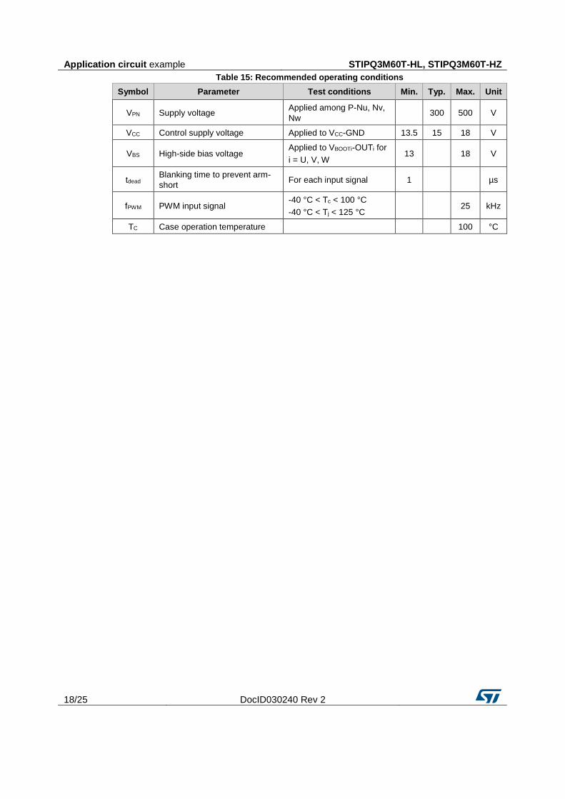
Table 15: Recommended operating conditions
Symbol Parameter Test conditions Min. Typ. Max. Unit
VPN Supply voltage Applied among P-Nu, Nv,
Nw 300 500 V
VCC Control supply voltage Applied to VCC-GND 13.5 15 18 V
VBS High-side bias voltage Applied to VBOOTi-OUTi for
i = U, V, W 13
18 V
tdead Blanking time to prevent arm-
short For each input signal 1
µs
fPWM PWM input signal -40 °C < Tc < 100 °C
-40 °C < Tj < 125 °C 25 kHz
TC Case operation temperature
100 °C
STIPQ3M60T-HL, STIPQ3M60T-HZ Package information
DocID030240 Rev 2 19/25
6 Package information
In order to meet environmental requirements, ST offers these devices in different grades of ECOPACK® packages, depending on their level of environmental compliance. ECOPACK® specifications, grade definitions and product status are available at: www.st.com. ECOPACK® is an ST trademark.
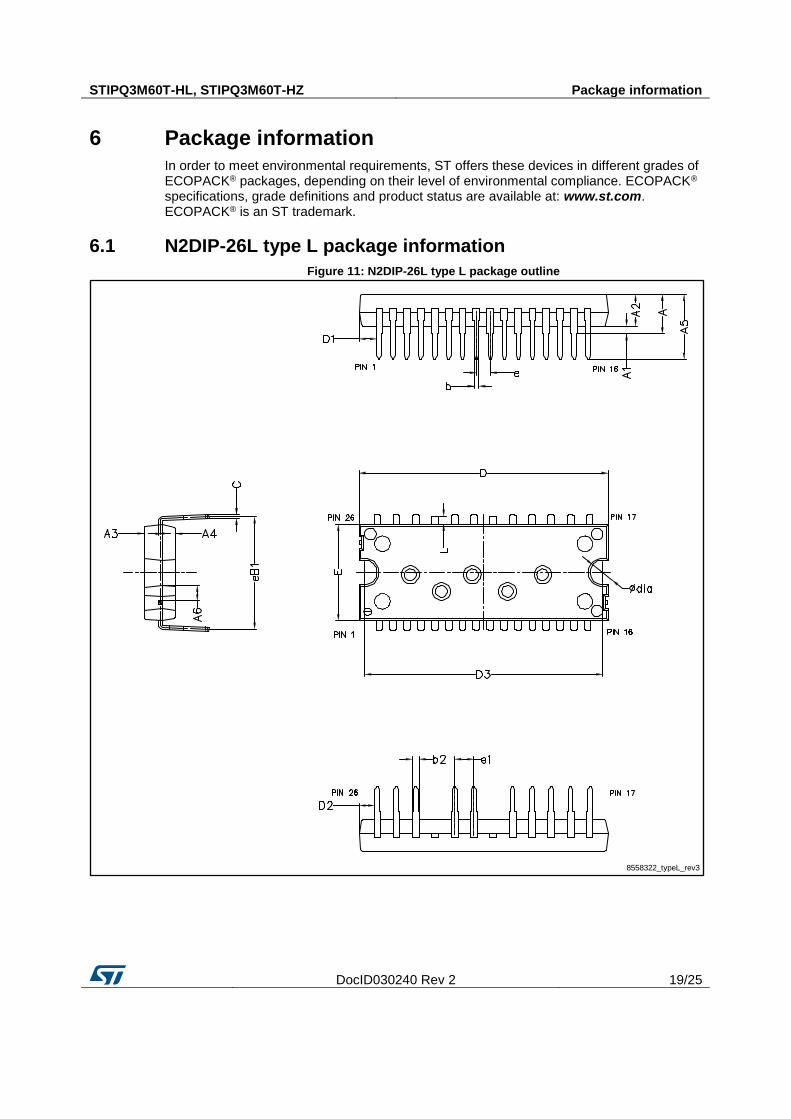
6.1 N2DIP-26L type L package information
Figure 11: N2DIP-26L type L package outline
8558322_typeL_rev3
Package information STIPQ3M60T-HL, STIPQ3M60T-HZ
20/25 DocID030240 Rev 2
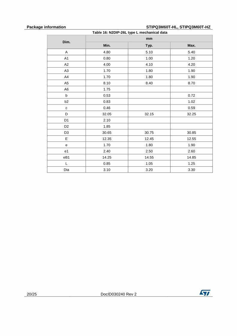
Table 16: N2DIP-26L type L mechanical data
Dim. mm
Min. Typ. Max.
A 4.80 5.10 5.40
A1 0.80 1.00 1.20
A2 4.00 4.10 4.20
A3 1.70 1.80 1.90
A4 1.70 1.80 1.90
A5 8.10 8.40 8.70
A6 1.75
b 0.53
0.72
b2 0.83
1.02
c 0.46
0.59
D 32.05 32.15 32.25
D1 2.10
D2 1.85
D3 30.65 30.75 30.85
E 12.35 12.45 12.55
e 1.70 1.80 1.90
e1 2.40 2.50 2.60
eB1 14.25 14.55 14.85
L 0.85 1.05 1.25
Dia 3.10 3.20 3.30
STIPQ3M60T-HL, STIPQ3M60T-HZ Package information
DocID030240 Rev 2 21/25
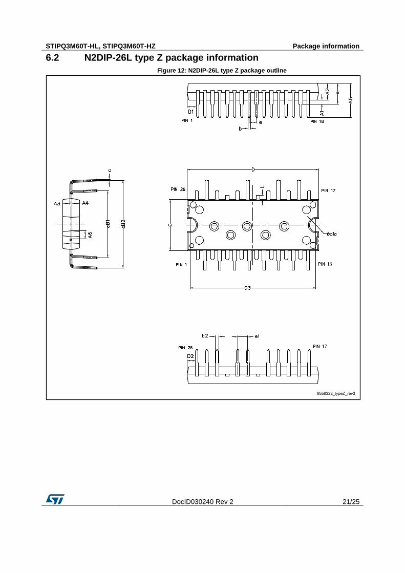
6.2 N2DIP-26L type Z package information
Figure 12: N2DIP-26L type Z package outline
8558322_typeZ_rev3
Package information STIPQ3M60T-HL, STIPQ3M60T-HZ
22/25 DocID030240 Rev 2
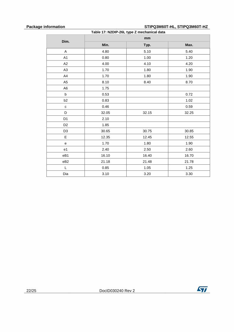
Table 17: N2DIP-26L type Z mechanical data
Dim. mm
Min. Typ. Max.
A 4.80 5.10 5.40
A1 0.80 1.00 1.20
A2 4.00 4.10 4.20
A3 1.70 1.80 1.90
A4 1.70 1.80 1.90
A5 8.10 8.40 8.70
A6 1.75
b 0.53
0.72
b2 0.83
1.02
c 0.46
0.59
D 32.05 32.15 32.25
D1 2.10
D2 1.85
D3 30.65 30.75 30.85
E 12.35 12.45 12.55
e 1.70 1.80 1.90
e1 2.40 2.50 2.60
eB1 16.10 16.40 16.70
eB2 21.18 21.48 21.78
L 0.85 1.05 1.25
Dia 3.10 3.20 3.30
STIPQ3M60T-HL, STIPQ3M60T-HZ Package information
DocID030240 Rev 2 23/25
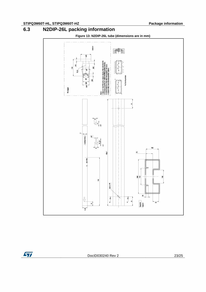
6.3 N2DIP-26L packing information
Figure 13: N2DIP-26L tube (dimensions are in mm)
Revision history STIPQ3M60T-HL, STIPQ3M60T-HZ
24/25 DocID030240 Rev 2
7 Revision history Table 18: Document revision history
Date Revision Changes
17-Jan-2017 1 Initial release.
27-Jun-2017 2
Document status promoted from preliminary data to production data.
Updated features in cover page.
Minor text changes.
STIPQ3M60T-HL, STIPQ3M60T-HZ
DocID030240 Rev 2 25/25
IMPORTANT NOTICE – PLEASE READ CAREFULLY
STMicroelectronics NV and its subsidiaries (“ST”) reserve the right to make changes, corrections, enhancements, modifications , and improvements to ST products and/or to this document at any time without notice. Purchasers should obtain the latest relevant information on ST products before placing orders. ST products are sold pursuant to ST’s terms and conditions of sale in place at the time of order acknowledgement.
Purchasers are solely responsible for the choice, selection, and use of ST products and ST assumes no liability for application assistance or the design of Purchasers’ products.
No license, express or implied, to any intellectual property right is granted by ST herein.
Resale of ST products with provisions different from the information set forth herein shall void any warranty granted by ST for such product.
ST and the ST logo are trademarks of ST. All other product or service names are the property of their respective owners.
Information in this document supersedes and replaces information previously supplied in any prior versions of this document.
© 2017 STMicroelectronics – All rights reserved