n CMOS Low Power Consumption - Your analog power … Ambient Temperature Topr -40~+85 Storage...
33
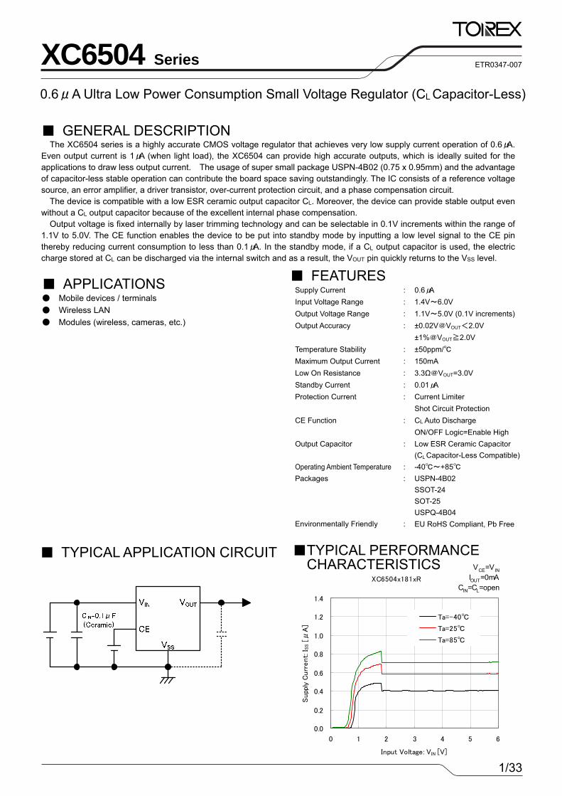
1/33 0.6μA Ultra Low Power Consumption Small Voltage Regulator (C L Capacitor-Less) XC6504 Series ■TYPICAL PERFORMANCE CHARACTERISTICS ■ GENERAL DESCRIPTION The XC6504 series is a highly accurate CMOS voltage regulator that achieves very low supply current operation of 0.6μ A. Even output current is 1μ A (when light load), the XC6504 can provide high accurate outputs, which is ideally suited for the applications to draw less output current. The usage of super small package USPN-4B02 (0.75 x 0.95mm) and the advantage of capacitor-less stable operation can contribute the board space saving outstandingly. The IC consists of a reference voltage source, an error amplifier, a driver transistor, over-current protection circuit, and a phase compensation circuit. The device is compatible with a low ESR ceramic output capacitor CL. Moreover, the device can provide stable output even without a CL output capacitor because of the excellent internal phase compensation. Output voltage is fixed internally by laser trimming technology and can be selectable in 0.1V increments within the range of 1.1V to 5.0V. The CE function enables the device to be put into standby mode by inputting a low level signal to the CE pin thereby reducing current consumption to less than 0.1μ A. In the standby mode, if a CL output capacitor is used, the electric charge stored at CL can be discharged via the internal switch and as a result, the VOUT pin quickly returns to the VSS level. ■ FEATURES Supply Current : 0.6μ A Input Voltage Range : 1.4V~6.0V Output Voltage Range : 1.1V~5.0V (0.1V increments) Output Accuracy : ±0.02V@V OUT <2.0V ±1%@V OUT ≧2.0V Temperature Stability : ±50ppm/℃ Maximum Output Current : 150mA Low On Resistance : 3.3Ω@V OUT =3.0V Standby Current : 0.01μ A Protection Current : Current Limiter Shot Circuit Protection CE Function : CL Auto Discharge ON/OFF Logic=Enable High Output Capacitor : Low ESR Ceramic Capacitor (C L Capacitor-Less Compatible) Operating Ambient Temperature : -40℃~+85℃ Packages : USPN-4B02 SSOT-24 SOT-25 USPQ-4B04 Environmentally Friendly : EU RoHS Compliant, Pb Free ■ TYPICAL APPLICATION CIRCUIT ETR0347-007 ■ APPLICATIONS ● Mobile devices / terminals ● Wireless LAN ● Modules (wireless, cameras, etc.) XC6504x181xR 0.0 0.2 0.4 0.6 0.8 1.0 1.2 1.4 0 1 2 3 4 5 6 Input Voltage: V IN [V] Supply Current: I SS [μA] Ta=-40℃ Ta=25℃ Ta=85℃ V CE =V IN I OUT =0mA C IN =C L =open
Transcript of n CMOS Low Power Consumption - Your analog power … Ambient Temperature Topr -40~+85 Storage...
1/33
0.6μA Ultra Low Power Consumption Small Voltage Regulator (CL Capacitor-Less)
XC6504 Series
TYPICAL PERFORMANCECHARACTERISTICS
GENERAL DESCRIPTION The XC6504 series is a highly accurate CMOS voltage regulator that achieves very low supply current operation of 0.6μA.
Even output current is 1μA (when light load), the XC6504 can provide high accurate outputs, which is ideally suited for the applications to draw less output current. The usage of super small package USPN-4B02 (0.75 x 0.95mm) and the advantage of capacitor-less stable operation can contribute the board space saving outstandingly. The IC consists of a reference voltage source, an error amplifier, a driver transistor, over-current protection circuit, and a phase compensation circuit.
The device is compatible with a low ESR ceramic output capacitor CL. Moreover, the device can provide stable output even without a CL output capacitor because of the excellent internal phase compensation.
Output voltage is fixed internally by laser trimming technology and can be selectable in 0.1V increments within the range of 1.1V to 5.0V. The CE function enables the device to be put into standby mode by inputting a low level signal to the CE pin thereby reducing current consumption to less than 0.1μA. In the standby mode, if a CL output capacitor is used, the electric charge stored at CL can be discharged via the internal switch and as a result, the VOUT pin quickly returns to the VSS level.
FEATURESSupply Current : 0.6μA Input Voltage Range : 1.4V~6.0V Output Voltage Range : 1.1V~5.0V (0.1V increments) Output Accuracy : ±0.02V@VOUT<2.0V
±1%@VOUT≧2.0V
Temperature Stability : ±50ppm/ Maximum Output Current : 150mA Low On Resistance : 3.3Ω@VOUT=3.0V Standby Current : 0.01μA Protection Current : Current Limiter Shot Circuit Protection CE Function : CL Auto Discharge ON/OFF Logic=Enable High Output Capacitor : Low ESR Ceramic Capacitor
(CL Capacitor-Less Compatible) Operating Ambient Temperature : -40~+85 Packages : USPN-4B02
SSOT-24 SOT-25 USPQ-4B04
Environmentally Friendly : EU RoHS Compliant, Pb Free
TYPICAL APPLICATION CIRCUIT
ETR0347-007
APPLICATIONS Mobile devices / terminals Wireless LAN Modules (wireless, cameras, etc.)
XC6504x181xR
0.0
0.2
0.4
0.6
0.8
1.0
1.2
1.4
0 1 2 3 4 5 6
Input Voltage: VIN [V]
Supp
ly C
urr
ent: I
SS [
μA
]
Ta=-40
Ta=25
Ta=85
VCE=VINIOUT=0mA
CIN=CL=open
2/33
XC6504 Series
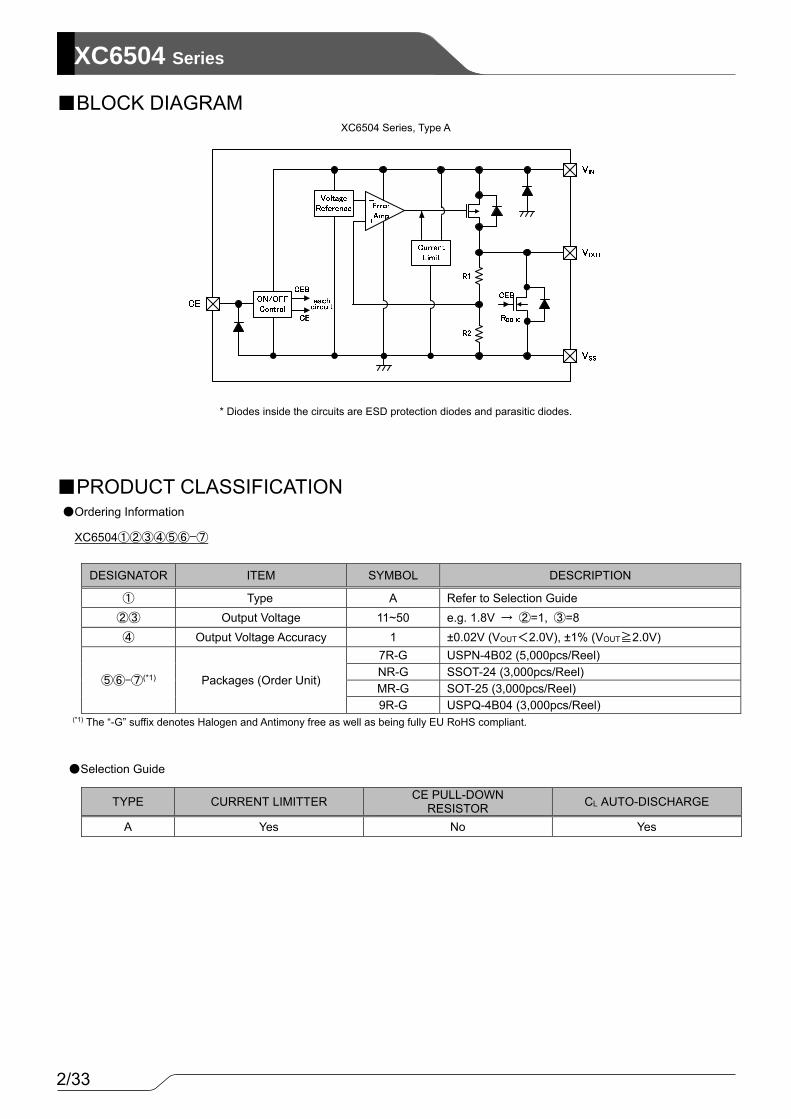
BLOCK DIAGRAM
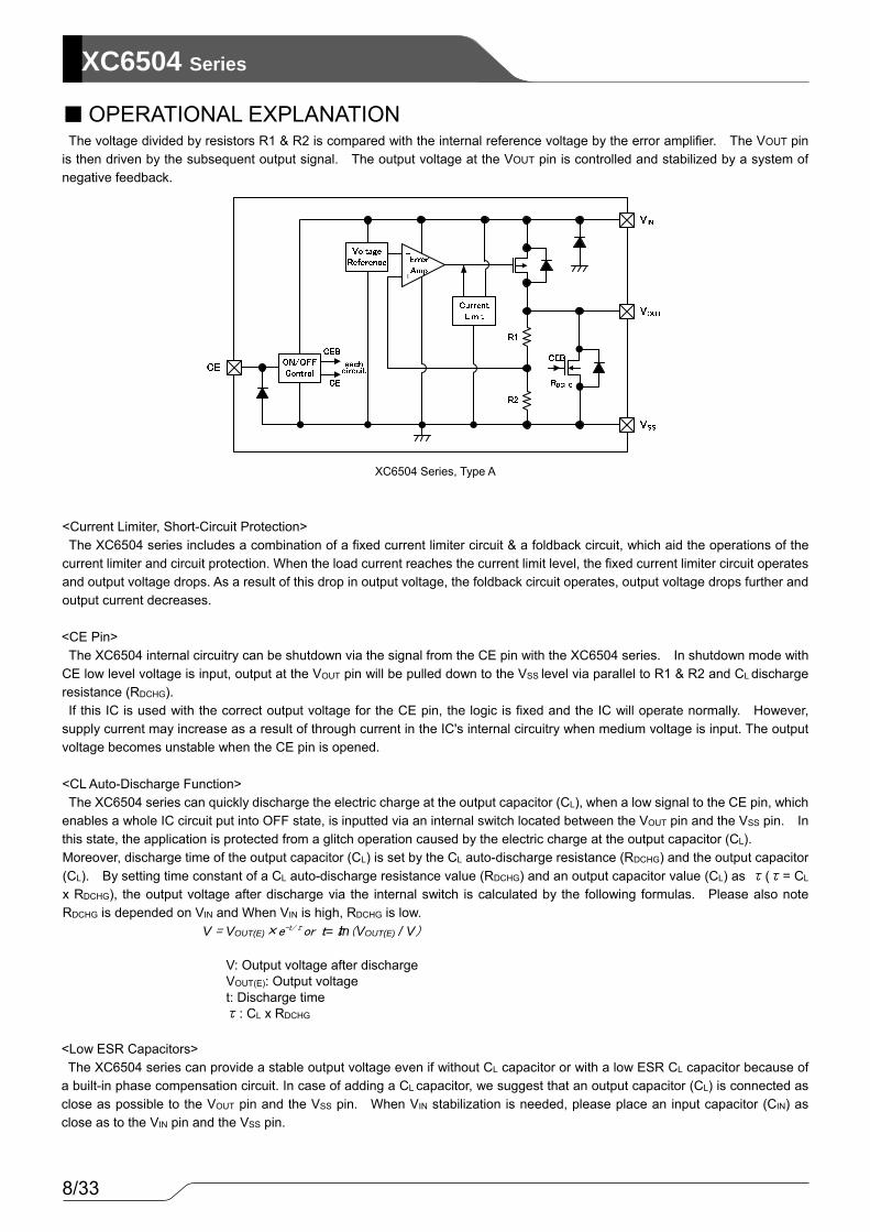
XC6504 Series, Type A
* Diodes inside the circuits are ESD protection diodes and parasitic diodes.
PRODUCT CLASSIFICATION
Ordering Information
XC6504①②③④⑤⑥-⑦
(*1) The “-G” suffix denotes Halogen and Antimony free as well as being fully EU RoHS compliant.
Selection Guide
DESIGNATOR ITEM SYMBOL DESCRIPTION
① Type A Refer to Selection Guide ②③ Output Voltage 11~50 e.g. 1.8V → ②=1, ③=8 ④ Output Voltage Accuracy 1 ±0.02V (VOUT<2.0V), ±1% (VOUT≧2.0V)
⑤⑥-⑦(*1) Packages (Order Unit)
7R-G USPN-4B02 (5,000pcs/Reel) NR-G SSOT-24 (3,000pcs/Reel) MR-G SOT-25 (3,000pcs/Reel) 9R-G USPQ-4B04 (3,000pcs/Reel)
TYPE CURRENT LIMITTER CE PULL-DOWN RESISTOR
CL AUTO-DISCHARGE
A Yes No Yes
3/33
XC6504Series
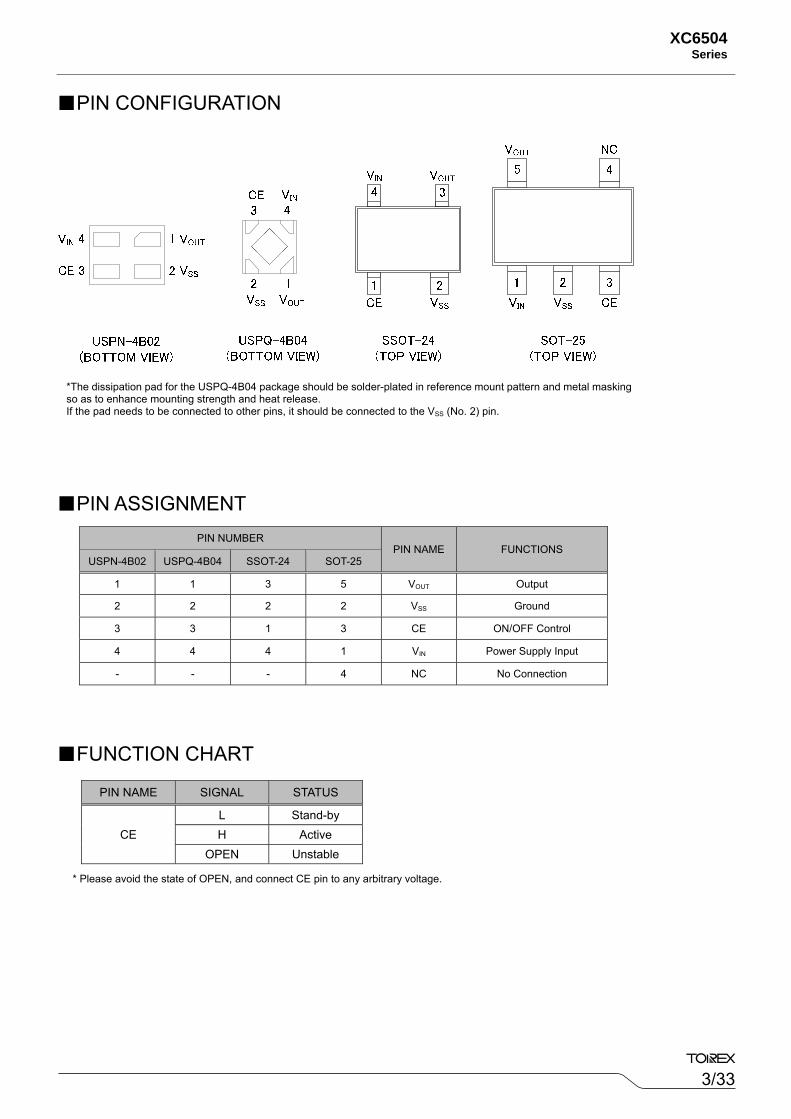
PIN CONFIGURATION
PIN ASSIGNMENT
FUNCTION CHART
* Please avoid the state of OPEN, and connect CE pin to any arbitrary voltage.
PIN NUMBER PIN NAME FUNCTIONS
USPN-4B02 USPQ-4B04 SSOT-24 SOT-25
1 1 3 5 VOUT Output
2 2 2 2 VSS Ground
3 3 1 3 CE ON/OFF Control
4 4 4 1 VIN Power Supply Input
- - - 4 NC No Connection
PIN NAME SIGNAL STATUS
CE
L Stand-by H Active
OPEN Unstable
*The dissipation pad for the USPQ-4B04 package should be solder-plated in reference mount pattern and metal masking so as to enhance mounting strength and heat release. If the pad needs to be connected to other pins, it should be connected to the VSS (No. 2) pin.
4/33
XC6504 Series
ABSOLUTE MAXIMUM RATINGS
All voltages are described based on the VSS.
(*1) Please use within the range of IOUT≦Pd / (VIN-VOUT) (*2) The maximum rating corresponds to the lowest value between VIN+0.3 or +6.5.
(*3) The power dissipation figure shown is PCB mounted and is for reference only Please see the power dissipation page for the mounting condition.
.
PARAMETER SYMBOL RATINGS UNITS
Input Voltage VIN -0.3~+6.5 V Output Current IOUT 470 (*1) mA Output Voltage VOUT -0.3~VIN+0.3 or +6.5 (*2) V
CE Input Voltage VCE -0.3~+6.5 V
Power Dissipation
USPQ-4B04
Pd
100
mW
550 (40mm x 40mm Standard board) (*3)
USPN-4B02 100
550 (40mm x 40mm Standard board) (*3)
SSOT-24 150
500 (40mm x 40mm Standard board) (*3)
SOT-25 250
600 (40mm x 40mm Standard board) (*3) Operating Ambient Temperature Topr -40~+85
Storage Temperature Tstg -55~+125
Ta=25
5/33
XC6504Series
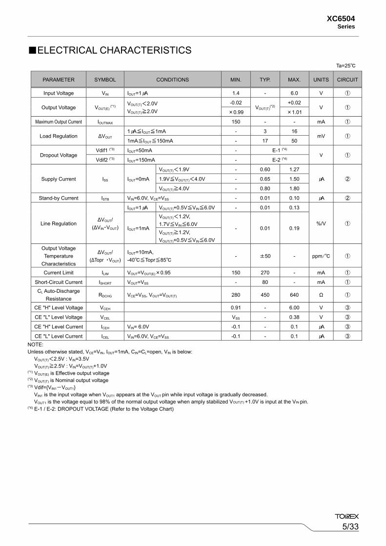
ELECTRICAL CHARACTERISTICS
NOTE: Unless otherwise stated, VCE=VIN, IOUT=1mA, CIN=CL=open, VIN is below:
VOUT(T)<2.5V : VIN=3.5V VOUT(T)≧2.5V : VIN=VOUT(T)+1.0V
(*1) VOUT(E) is Effective output voltage (*2) VOUT(T) is Nominal output voltage (*3) Vdif=VIN1-VOUT1
VIN1 is the input voltage when VOUT1 appears at the VOUT pin while input voltage is gradually decreased. VOUT1 is the voltage equal to 98% of the normal output voltage when amply stabilized VOUT(T) +1.0V is input at the VIN pin.
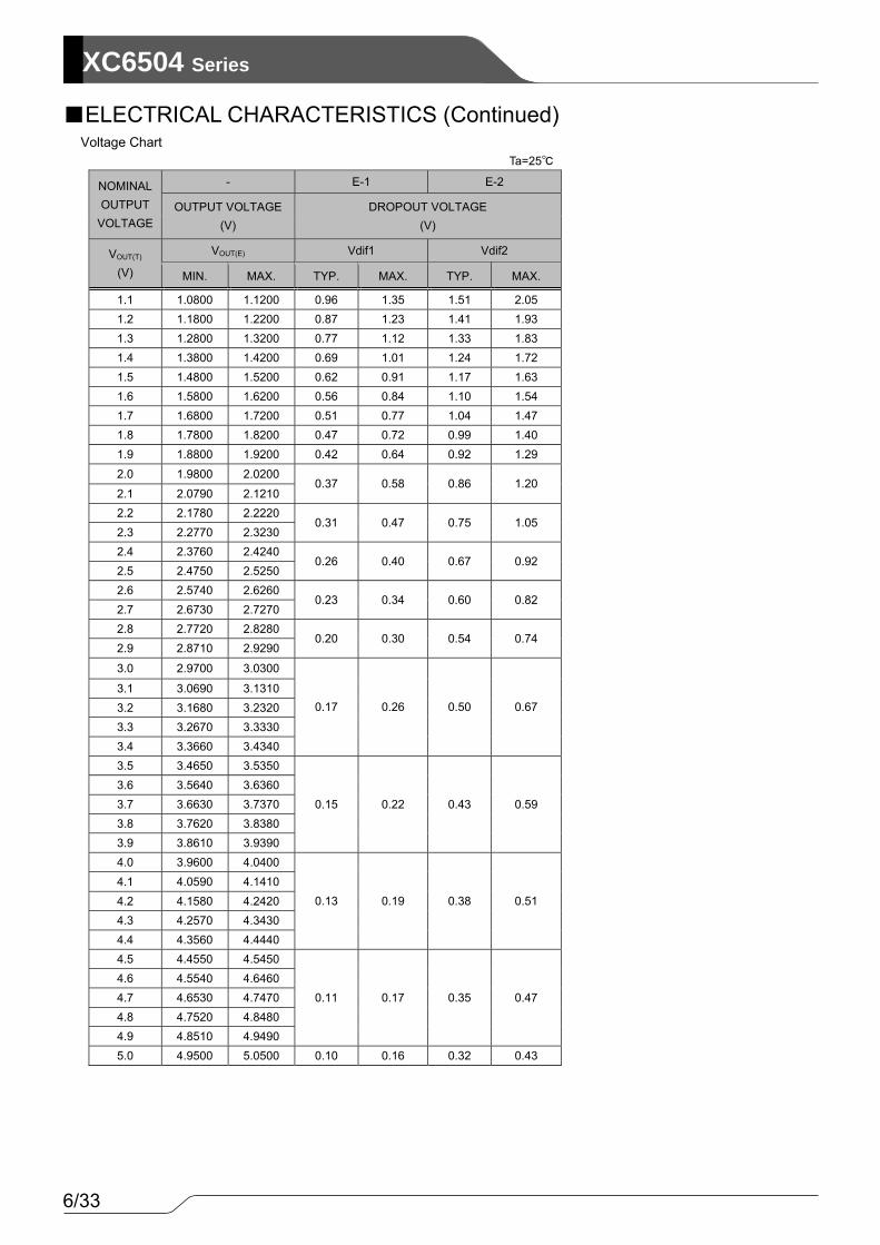
(*4) E-1 / E-2: DROPOUT VOLTAGE (Refer to the Voltage Chart)
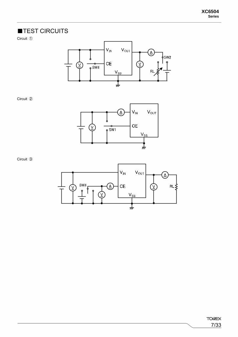
PARAMETER SYMBOL CONDITIONS MIN. TYP. MAX. UNITS CIRCUIT
Input Voltage VIN IOUT=1μA 1.4 - 6.0 V ①
Output Voltage VOUT(E) (*1)
VOUT(T)<2.0V VOUT(T)≧2.0V
-0.02 VOUT(T)
(*2) +0.02
V ① ×0.99 ×1.01
Maximum Output Current IOUTMAX 150 - - mA ①
Load Regulation ∆VOUT 1μA≦IOUT≦1mA - 3 16
mV ① 1mA≦IOUT≦150mA - 17 50
Dropout Voltage Vdif1 (*3) IOUT=50mA - E-1 (*4)
V ① Vdif2 (*3) IOUT=150mA - E-2 (*4)
Supply Current ISS IOUT=0mA
VOUT(T)<1.9V - 0.60 1.27
μA ② 1.9V≦VOUT(T)<4.0V - 0.65 1.50
VOUT(T)≧4.0V - 0.80 1.80
Stand-by Current ISTB VIN=6.0V, VCE=VSS - 0.01 0.10 μA ②
Line Regulation ∆VOUT/
(∆VIN・VOUT)
IOUT=1μA VOUT(T)+0.5V≦VIN≦6.0V - 0.01 0.13
%/V ① IOUT=1mA
VOUT(T)<1.2V, 1.7V≦VIN≦6.0V
- 0.01 0.19 VOUT(T)≧1.2V, VOUT(T)+0.5V≦VIN≦6.0V
Output Voltage Temperature
Characteristics
∆VOUT/ (∆Topr ・VOUT)
IOUT=10mA, -40≦Topr≦85
- ±50 - ppm/ ①
Current Limit ILIM VOUT=VOUT(E)×0.95 150 270 - mA ①
Short-Circuit Current ISHORT VOUT=VSS - 80 - mA ①
CL Auto-Discharge Resistance
RDCHG VCE=VSS, VOUT=VOUT(T) 280 450 640 Ω ①
CE "H" Level Voltage VCEH 0.91 - 6.00 V ③
CE "L" Level Voltage VCEL VSS - 0.38 V ③
CE "H" Level Current ICEH VIN= 6.0V -0.1 - 0.1 μA ③
CE "L" Level Current ICEL VIN=6.0V, VCE=VSS -0.1 - 0.1 μA ③
Ta=25
6/33
XC6504 Series
ELECTRICAL CHARACTERISTICS (Continued)
Voltage Chart
NOMINAL OUTPUT
VOLTAGE
- E-1 E-2
OUTPUT VOLTAGE (V)
DROPOUT VOLTAGE (V)
VOUT(T)
(V)
VOUT(E) Vdif1 Vdif2
MIN. MAX. TYP. MAX. TYP. MAX.
1.1 1.0800 1.1200 0.96 1.35 1.51 2.05 1.2 1.1800 1.2200 0.87 1.23 1.41 1.93 1.3 1.2800 1.3200 0.77 1.12 1.33 1.83 1.4 1.3800 1.4200 0.69 1.01 1.24 1.72 1.5 1.4800 1.5200 0.62 0.91 1.17 1.63 1.6 1.5800 1.6200 0.56 0.84 1.10 1.54 1.7 1.6800 1.7200 0.51 0.77 1.04 1.47 1.8 1.7800 1.8200 0.47 0.72 0.99 1.40 1.9 1.8800 1.9200 0.42 0.64 0.92 1.29
2.0 1.9800 2.0200 0.37 0.58 0.86 1.20
2.1 2.0790 2.1210 2.2 2.1780 2.2220
0.31 0.47 0.75 1.05 2.3 2.2770 2.3230 2.4 2.3760 2.4240
0.26 0.40 0.67 0.92 2.5 2.4750 2.5250 2.6 2.5740 2.6260
0.23 0.34 0.60 0.82 2.7 2.6730 2.7270 2.8 2.7720 2.8280
0.20 0.30 0.54 0.74 2.9 2.8710 2.9290
3.0 2.9700 3.0300
0.17 0.26 0.50 0.67 3.1 3.0690 3.1310 3.2 3.1680 3.2320 3.3 3.2670 3.3330 3.4 3.3660 3.4340 3.5 3.4650 3.5350
0.15 0.22 0.43 0.59 3.6 3.5640 3.6360 3.7 3.6630 3.7370 3.8 3.7620 3.8380 3.9 3.8610 3.9390 4.0 3.9600 4.0400
0.13 0.19 0.38 0.51 4.1 4.0590 4.1410 4.2 4.1580 4.2420 4.3 4.2570 4.3430 4.4 4.3560 4.4440 4.5 4.4550 4.5450
0.11 0.17 0.35 0.47 4.6 4.5540 4.6460 4.7 4.6530 4.7470 4.8 4.7520 4.8480 4.9 4.8510 4.9490 5.0 4.9500 5.0500 0.10 0.16 0.32 0.43
Ta=25
7/33
XC6504Series
TEST CIRCUITS
Circuit ① Circuit ②
Circuit ③
8/33
XC6504 Series
OPERATIONAL EXPLANATION The voltage divided by resistors R1 & R2 is compared with the internal reference voltage by the error amplifier. The VOUT pin
is then driven by the subsequent output signal. The output voltage at the VOUT pin is controlled and stabilized by a system of negative feedback.
XC6504 Series, Type A
<Current Limiter, Short-Circuit Protection> The XC6504 series includes a combination of a fixed current limiter circuit & a foldback circuit, which aid the operations of the
current limiter and circuit protection. When the load current reaches the current limit level, the fixed current limiter circuit operates and output voltage drops. As a result of this drop in output voltage, the foldback circuit operates, output voltage drops further and output current decreases. <CE Pin> The XC6504 internal circuitry can be shutdown via the signal from the CE pin with the XC6504 series. In shutdown mode with
CE low level voltage is input, output at the VOUT pin will be pulled down to the VSS level via parallel to R1 & R2 and CL discharge resistance (RDCHG). If this IC is used with the correct output voltage for the CE pin, the logic is fixed and the IC will operate normally. However,
supply current may increase as a result of through current in the IC's internal circuitry when medium voltage is input. The output voltage becomes unstable when the CE pin is opened. <CL Auto-Discharge Function> The XC6504 series can quickly discharge the electric charge at the output capacitor (CL), when a low signal to the CE pin, which
enables a whole IC circuit put into OFF state, is inputted via an internal switch located between the VOUT pin and the VSS pin. In this state, the application is protected from a glitch operation caused by the electric charge at the output capacitor (CL). Moreover, discharge time of the output capacitor (CL) is set by the CL auto-discharge resistance (RDCHG) and the output capacitor (CL). By setting time constant of a CL auto-discharge resistance value (RDCHG) and an output capacitor value (CL) as τ(τ= CL x RDCHG), the output voltage after discharge via the internal switch is calculated by the following formulas. Please also note RDCHG is depended on VIN and When VIN is high, RDCHG is low. V = VOUT(E)×e-t/τ or t=τln(VOUT(E) / V)
V: Output voltage after discharge VOUT(E): Output voltage t: Discharge time τ: CL x RDCHG <Low ESR Capacitors> The XC6504 series can provide a stable output voltage even if without CL capacitor or with a low ESR CL capacitor because of
a built-in phase compensation circuit. In case of adding a CL capacitor, we suggest that an output capacitor (CL) is connected as close as possible to the VOUT pin and the VSS pin. When VIN stabilization is needed, please place an input capacitor (CIN) as close as to the VIN pin and the VSS pin.
9/33
XC6504Series
NOTES ON USE 1. For temporary, transitional voltage drop or voltage rising phenomenon, the IC is liable to malfunction should the ratings be
exceeded. 2. Where wiring impedance is high, operations may become unstable due to noise and/or phase lag depending on output current.
Please keep the resistance low between VIN and VSS wiring in particular. 3. Please wire the input capacitor (CIN) and the output capacitor (CL) as close to the IC as possible. 4. Capacitances of these capacitors (CIN, CL) are decreased by the influences of bias voltage and ambient temperature. Care shall
be taken for capacitor selection to ensure stability of phase compensation from the point of ESR influence. 5. Torex places an importance on improving our products and their reliability.
We request that users incorporate fail-safe designs and post-aging prevention treatment when using Torex products in their systems.
10/33
XC6504 Series
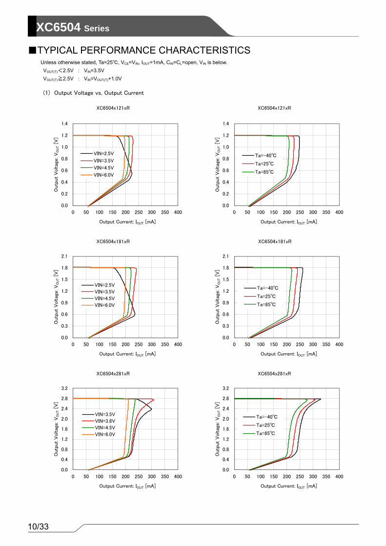
(1) Output Voltage vs. Output Current
XC6504x121xR
0.0
0.2
0.4
0.6
0.8
1.0
1.2
1.4
0 50 100 150 200 250 300 350 400
Output Current: IOUT [mA]
Outp
ut
Voltag
e: V
OU
T [
V]
VIN=2.5V
VIN=3.5V
VIN=4.5V
VIN=6.0V
XC6504x121xR
0.0
0.2
0.4
0.6
0.8
1.0
1.2
1.4
0 50 100 150 200 250 300 350 400
Output Current: IOUT [mA]O
utp
ut
Voltag
e: V
OU
T [
V]
Ta=-40
Ta=25
Ta=85
XC6504x181xR
0.0
0.3
0.6
0.9
1.2
1.5
1.8
2.1
0 50 100 150 200 250 300 350 400
Output Current: IOUT [mA]
Outp
ut
Voltag
e: V
OU
T [
V]
VIN=2.5V
VIN=3.5V
VIN=4.5V
VIN=6.0V
XC6504x181xR
0.0
0.3
0.6
0.9
1.2
1.5
1.8
2.1
0 50 100 150 200 250 300 350 400
Output Current: IOUT [mA]
Outp
ut
Voltag
e: V
OU
T [
V]
Ta=-40
Ta=25
Ta=85
XC6504x281xR
0.0
0.4
0.8
1.2
1.6
2.0
2.4
2.8
3.2
0 50 100 150 200 250 300 350 400
Output Current: IOUT [mA]
Outp
ut
Voltag
e: V
OU
T [
V]
VIN=3.5V
VIN=3.8V
VIN=4.5V
VIN=6.0V
XC6504x281xR
0.0
0.4
0.8
1.2
1.6
2.0
2.4
2.8
3.2
0 50 100 150 200 250 300 350 400
Output Current: IOUT [mA]
Outp
ut
Voltag
e: V
OU
T [
V]
Ta=-40
Ta=25
Ta=85
TYPICAL PERFORMANCE CHARACTERISTICS
Unless otherwise stated, Ta=25, VCE=VIN, IOUT=1mA, CIN=CL=open, VIN is below. VOUT(T)<2.5V : VIN=3.5V VOUT(T)≧2.5V : VIN=VOUT(T)+1.0V
11/33
XC6504Series
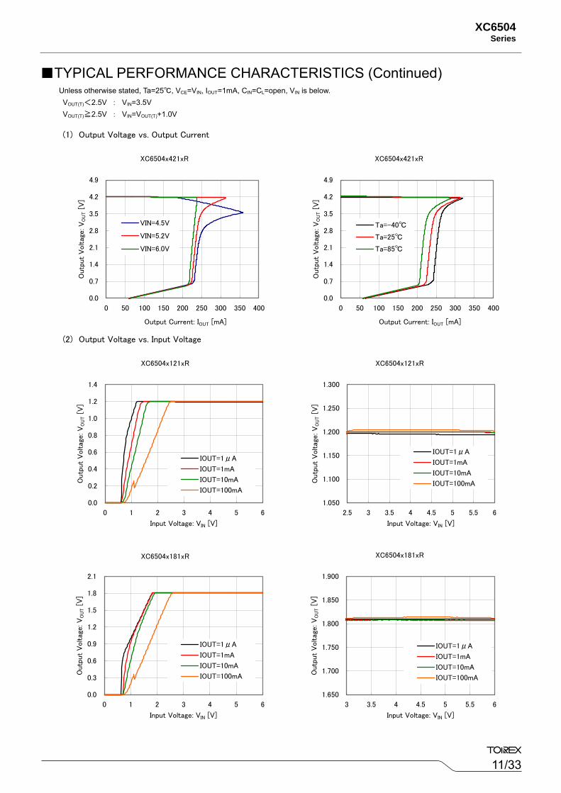
(1) Output Voltage vs. Output Current
(2) Output Voltage vs. Input Voltage
XC6504x421xR
0.0
0.7
1.4
2.1
2.8
3.5
4.2
4.9
0 50 100 150 200 250 300 350 400
Output Current: IOUT [mA]
Outp
ut
Voltag
e: V
OU
T [
V]
VIN=4.5V
VIN=5.2V
VIN=6.0V
XC6504x421xR
0.0
0.7
1.4
2.1
2.8
3.5
4.2
4.9
0 50 100 150 200 250 300 350 400
Output Current: IOUT [mA]O
utp
ut
Voltag
e: V
OU
T [
V]
Ta=-40
Ta=25
Ta=85
XC6504x121xR
0.0
0.2
0.4
0.6
0.8
1.0
1.2
1.4
0 1 2 3 4 5 6
Input Voltage: VIN [V]
Outp
ut
Voltag
e: V
OU
T [
V]
IOUT=1μA
IOUT=1mA
IOUT=10mA
IOUT=100mA
XC6504x121xR
1.050
1.100
1.150
1.200
1.250
1.300
2.5 3 3.5 4 4.5 5 5.5 6
Input Voltage: VIN [V]
Outp
ut
Voltag
e: V
OU
T [
V]
IOUT=1μA
IOUT=1mA
IOUT=10mA
IOUT=100mA
XC6504x181xR
0.0
0.3
0.6
0.9
1.2
1.5
1.8
2.1
0 1 2 3 4 5 6
Input Voltage: VIN [V]
Outp
ut
Voltag
e: V
OU
T [
V]
IOUT=1μA
IOUT=1mA
IOUT=10mA
IOUT=100mA
XC6504x181xR
1.650
1.700
1.750
1.800
1.850
1.900
3 3.5 4 4.5 5 5.5 6
Input Voltage: VIN [V]
Outp
ut
Voltag
e: V
OU
T [
V]
IOUT=1μA
IOUT=1mA
IOUT=10mA
IOUT=100mA
TYPICAL PERFORMANCE CHARACTERISTICS (Continued)
Unless otherwise stated, Ta=25, VCE=VIN, IOUT=1mA, CIN=CL=open, VIN is below. VOUT(T)<2.5V : VIN=3.5V VOUT(T)≧2.5V : VIN=VOUT(T)+1.0V
12/33
XC6504 Series
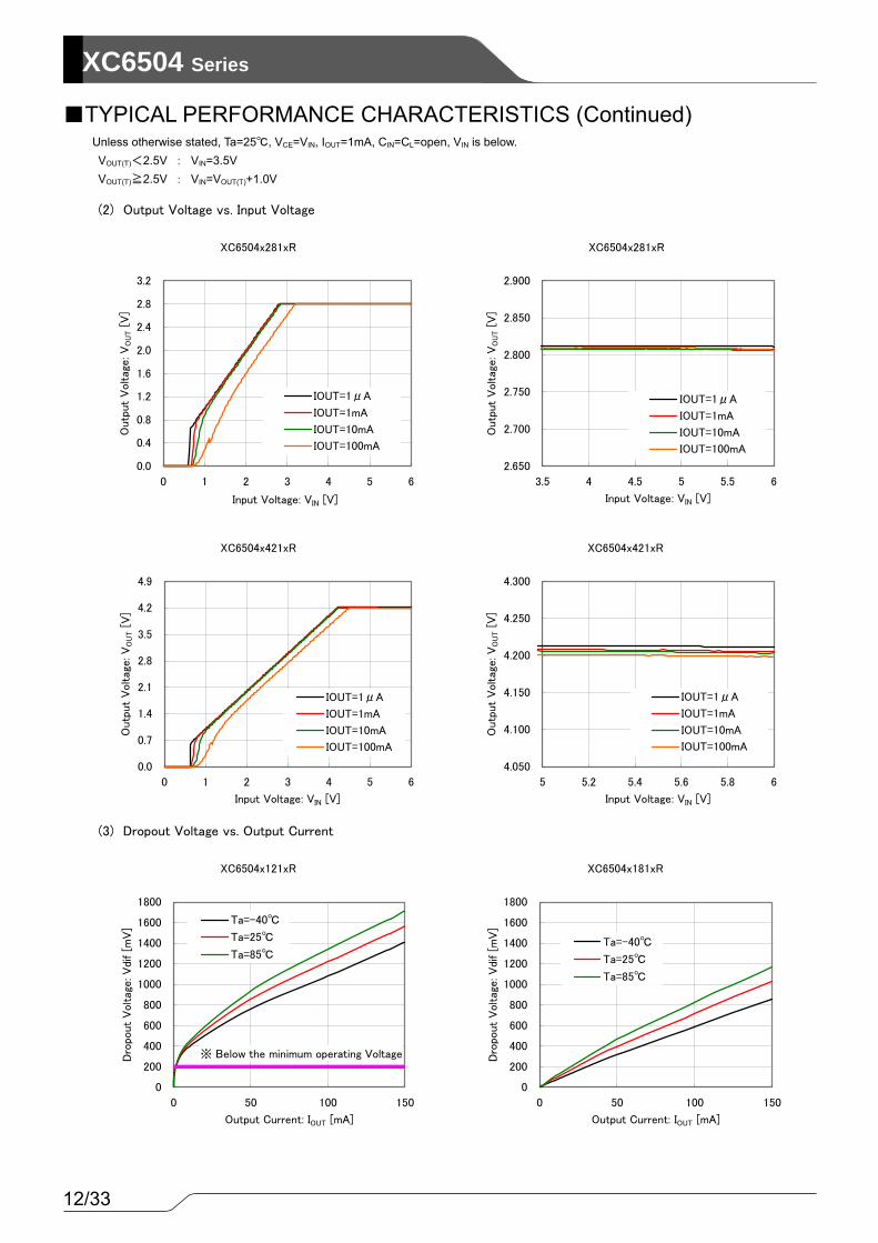
(2) Output Voltage vs. Input Voltage
(3) Dropout Voltage vs. Output Current
XC6504x281xR
0.0
0.4
0.8
1.2
1.6
2.0
2.4
2.8
3.2
0 1 2 3 4 5 6
Input Voltage: VIN [V]
Outp
ut
Voltag
e: V
OU
T [
V]
IOUT=1μA
IOUT=1mA
IOUT=10mA
IOUT=100mA
XC6504x281xR
2.650
2.700
2.750
2.800
2.850
2.900
3.5 4 4.5 5 5.5 6
Input Voltage: VIN [V]O
utp
ut
Voltag
e: V
OU
T [
V]
IOUT=1μA
IOUT=1mA
IOUT=10mA
IOUT=100mA
XC6504x421xR
0.0
0.7
1.4
2.1
2.8
3.5
4.2
4.9
0 1 2 3 4 5 6
Input Voltage: VIN [V]
Outp
ut
Voltag
e: V
OU
T [
V]
IOUT=1μA
IOUT=1mA
IOUT=10mA
IOUT=100mA
XC6504x421xR
4.050
4.100
4.150
4.200
4.250
4.300
5 5.2 5.4 5.6 5.8 6
Input Voltage: VIN [V]
Outp
ut
Voltag
e: V
OU
T [
V]
IOUT=1μA
IOUT=1mA
IOUT=10mA
IOUT=100mA
XC6504x121xR
0
200
400
600
800
1000
1200
1400
1600
1800
0 50 100 150
Output Current: IOUT [mA]
Dro
pout
Voltag
e: V
dif [m
V]
Ta=-40
Ta=25
Ta=85
※ Below the minimum operating Voltage
XC6504x181xR
0
200
400
600
800
1000
1200
1400
1600
1800
0 50 100 150
Output Current: IOUT [mA]
Dro
pout
Voltag
e: V
dif [m
V]
Ta=-40
Ta=25
Ta=85
TYPICAL PERFORMANCE CHARACTERISTICS (Continued)
Unless otherwise stated, Ta=25, VCE=VIN, IOUT=1mA, CIN=CL=open, VIN is below. VOUT(T)<2.5V : VIN=3.5V VOUT(T)≧2.5V : VIN=VOUT(T)+1.0V
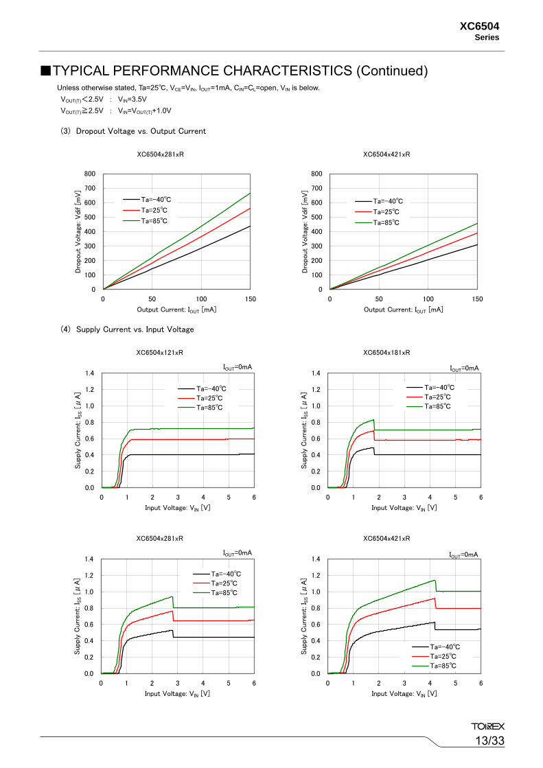
13/33
XC6504Series
(3) Dropout Voltage vs. Output Current
(4) Supply Current vs. Input Voltage
XC6504x281xR
0
100
200
300
400
500
600
700
800
0 50 100 150
Output Current: IOUT [mA]
Dro
pout
Voltag
e: V
dif [m
V]
Ta=-40
Ta=25
Ta=85
XC6504x421xR
0
100
200
300
400
500
600
700
800
0 50 100 150
Output Current: IOUT [mA]D
ropo
ut
Voltag
e: V
dif [m
V]
Ta=-40
Ta=25
Ta=85
XC6504x121xR
0.0
0.2
0.4
0.6
0.8
1.0
1.2
1.4
0 1 2 3 4 5 6
Input Voltage: VIN [V]
Suppl
y C
urr
ent: I
SS [
μA
] Ta=-40
Ta=25
Ta=85
IOUT=0mA
XC6504x181xR
0.0
0.2
0.4
0.6
0.8
1.0
1.2
1.4
0 1 2 3 4 5 6
Input Voltage: VIN [V]
Suppl
y C
urr
ent: I
SS [
μA
]
Ta=-40
Ta=25
Ta=85
IOUT=0mA
XC6504x281xR
0.0
0.2
0.4
0.6
0.8
1.0
1.2
1.4
0 1 2 3 4 5 6
Input Voltage: VIN [V]
Supp
ly C
urr
ent: I
SS [
μA
]
Ta=-40
Ta=25
Ta=85
IOUT=0mA
XC6504x421xR
0.0
0.2
0.4
0.6
0.8
1.0
1.2
1.4
0 1 2 3 4 5 6
Input Voltage: VIN [V]
Supp
ly C
urr
ent: I
SS [
μA
]
Ta=-40
Ta=25
Ta=85
IOUT=0mA
TYPICAL PERFORMANCE CHARACTERISTICS (Continued)
Unless otherwise stated, Ta=25, VCE=VIN, IOUT=1mA, CIN=CL=open, VIN is below. VOUT(T)<2.5V : VIN=3.5V VOUT(T)≧2.5V : VIN=VOUT(T)+1.0V
14/33
XC6504 Series
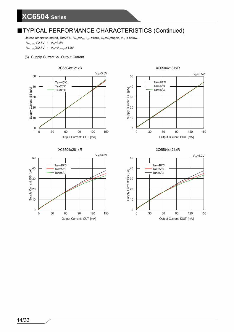
TYPICAL PERFORMANCE CHARACTERISTICS (Continued)
Unless otherwise stated, Ta=25, VCE=VIN, IOUT=1mA, CIN=CL=open, VIN is below. VOUT(T)<2.5V : VIN=3.5V VOUT(T)≧2.5V : VIN=VOUT(T)+1.0V
(5) Supply Current vs. Output Current
0
10
20
30
40
50
0 30 60 90 120 150
Supp
ly C
urre
nt: IS
S [μ
A]
Output Current: IOUT [mA]
XC6504x121xR
Ta=-40Ta=25Ta=85
VIN=3.5V
0
10
20
30
40
50
0 30 60 90 120 150Su
pply
Cur
rent
: ISS
[μA
]
Output Current: IOUT [mA]
XC6504x181xR
Ta=-40Ta=25Ta=85
VIN=3.5V
0
10
20
30
40
50
0 30 60 90 120 150
Supp
ly C
urre
nt: IS
S [μ
A]
Output Current: IOUT [mA]
XC6504x281xR
Ta=-40Ta=25Ta=85
VIN=3.8V
0
10
20
30
40
50
0 30 60 90 120 150
Supp
ly C
urre
nt: IS
S [μ
A]
Output Current: IOUT [mA]
XC6504x421xR
Ta=-40Ta=25Ta=85
VIN=5.2V
15/33
XC6504Series
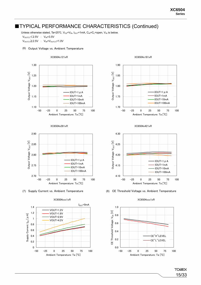
(5) Output Voltage vs. Ambient Temperature
(6) Supply Current vs. Ambient Temperature (7) CE Threshold Voltage vs. Ambient Temperature
XC6504x121xR
1.10
1.15
1.20
1.25
1.30
-50 -25 0 25 50 75 100
Ambient Temperature: Ta []
Outp
ut
Voltag
e: V
OU
T [
V]
IOUT=1μA
IOUT=1mA
IOUT=10mA
IOUT=100mA
XC6504x181xR
1.70
1.75
1.80
1.85
1.90
-50 -25 0 25 50 75 100
Ambient Temperature: Ta []O
utp
ut
Voltag
e: V
OU
T [
V]
IOUT=1μA
IOUT=1mA
IOUT=10mA
IOUT=100mA
XC6504x281xR
2.70
2.75
2.80
2.85
2.90
-50 -25 0 25 50 75 100
Ambient Temperature: Ta []
Outp
ut
Voltag
e: V
OU
T [
V]
IOUT=1μA
IOUT=1mA
IOUT=10mA
IOUT=100mA
XC6504x421xR
4.10
4.15
4.20
4.25
4.30
-50 -25 0 25 50 75 100
Ambient Temperature: Ta []
Outp
ut
Voltag
e: V
OU
T [
V]
IOUT=1μA
IOUT=1mA
IOUT=10mA
IOUT=100mA
XC6504xxx1xR
0
0.2
0.4
0.6
0.8
1
1.2
1.4
-50 -25 0 25 50 75 100
Ambient Temperature: Ta []
Supp
ly C
urr
ent: I
SS [
μA
]
VOUT=1.2V
VOUT=1.8V
VOUT=2.8VVOUT=4.2V
IOUT=0mA
XC6504xxx1xR
0.0
0.2
0.4
0.6
0.8
1.0
-50 -25 0 25 50 75 100
Ambient Temperature: Ta []
CE T
hre
shold
Voltag
e: V
CE [
V]
CE"H"LEVEL
CE"L"LEVEL
TYPICAL PERFORMANCE CHARACTERISTICS (Continued)
Unless otherwise stated, Ta=25, VCE=VIN, IOUT=1mA, CIN=CL=open, VIN is below. VOUT(T)<2.5V : VIN=3.5V VOUT(T)≧2.5V : VIN=VOUT(T)+1.0V
(6)
(7) (8)
16/33
XC6504 Series
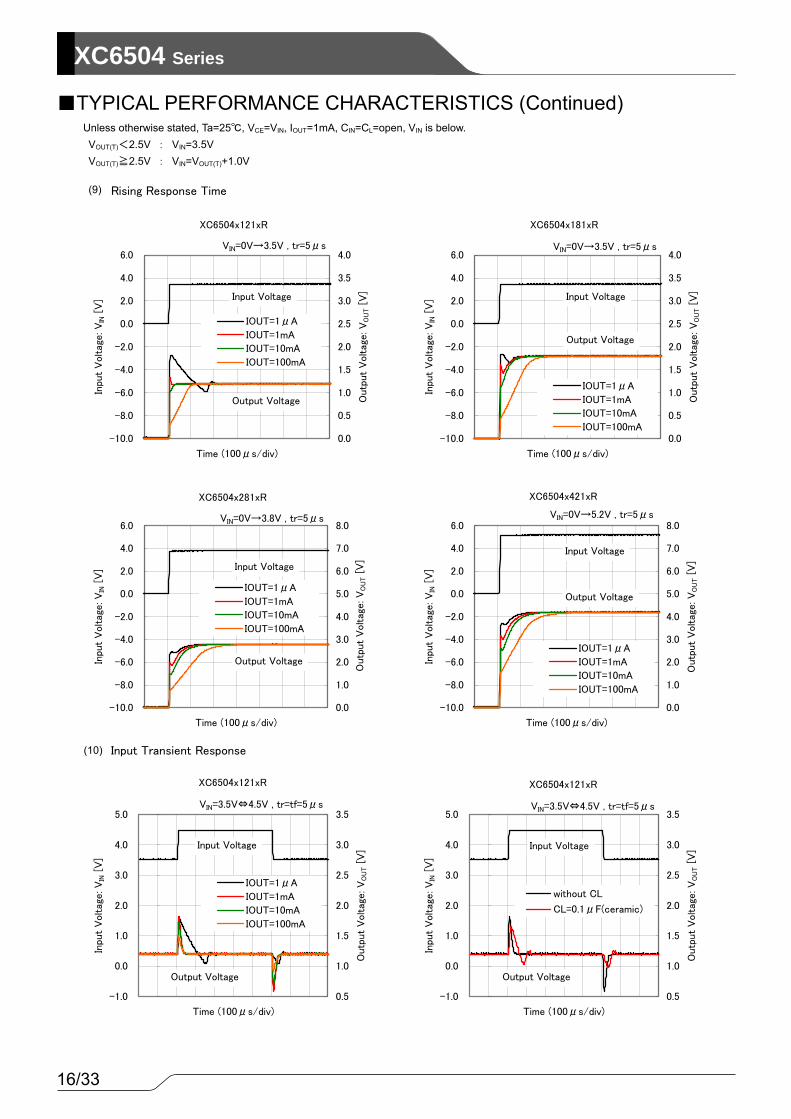
(8) Rising Response Time
(9) Input Transient Response
XC6504x281xR
-10.0
-8.0
-6.0
-4.0
-2.0
0.0
2.0
4.0
6.0
Time (100μs/div)
Inpu
t V
oltag
e: V
IN [
V]
0.0
1.0
2.0
3.0
4.0
5.0
6.0
7.0
8.0
Outp
ut
Voltag
e: V
OU
T [
V]
IOUT=1μA
IOUT=1mA
IOUT=10mA
IOUT=100mA
VIN=0V→3.8V , tr=5μs
Input Voltage
Output Voltage
XC6504x421xR
-10.0
-8.0
-6.0
-4.0
-2.0
0.0
2.0
4.0
6.0
Time (100μs/div)
Inpu
t V
oltag
e: V
IN [
V]
0.0
1.0
2.0
3.0
4.0
5.0
6.0
7.0
8.0
Outp
ut
Voltag
e: V
OU
T [
V]
IOUT=1μA
IOUT=1mA
IOUT=10mA
IOUT=100mA
Input Voltage
Output Voltage
VIN=0V→5.2V , tr=5μs
XC6504x121xR
-1.0
0.0
1.0
2.0
3.0
4.0
5.0
Time (100μs/div)
Inpu
t V
oltag
e: V
IN [
V]
0.5
1.0
1.5
2.0
2.5
3.0
3.5
Outp
ut
Voltag
e: V
OU
T [
V]
IOUT=1μA
IOUT=1mA
IOUT=10mA
IOUT=100mA
VIN=3.5V⇔4.5V , tr=tf=5μs
Input Voltage
Output Voltage
XC6504x121xR
-1.0
0.0
1.0
2.0
3.0
4.0
5.0
Time (100μs/div)
Inpu
t V
oltag
e: V
IN [
V]
0.5
1.0
1.5
2.0
2.5
3.0
3.5
Outp
ut
Voltag
e: V
OU
T [
V]
without CL
CL=0.1μF(ceramic)
VIN=3.5V⇔4.5V , tr=tf=5μs
Input Voltage
Output Voltage
XC6504x121xR
-10.0
-8.0
-6.0
-4.0
-2.0
0.0
2.0
4.0
6.0
Time (100μs/div)
Inpu
t V
oltag
e: V
IN [
V]
0.0
0.5
1.0
1.5
2.0
2.5
3.0
3.5
4.0
Outp
ut
Voltag
e: V
OU
T [
V]
IOUT=1μA
IOUT=1mA
IOUT=10mA
IOUT=100mA
VIN=0V→3.5V , tr=5μs
Input Voltage
Output Voltage
XC6504x181xR
-10.0
-8.0
-6.0
-4.0
-2.0
0.0
2.0
4.0
6.0
Time (100μs/div)
Inpu
t V
oltag
e: V
IN [
V]
0.0
0.5
1.0
1.5
2.0
2.5
3.0
3.5
4.0
Outp
ut
Voltag
e: V
OU
T [
V]
IOUT=1μA
IOUT=1mA
IOUT=10mA
IOUT=100mA
VIN=0V→3.5V , tr=5μs
Input Voltage
Output Voltage
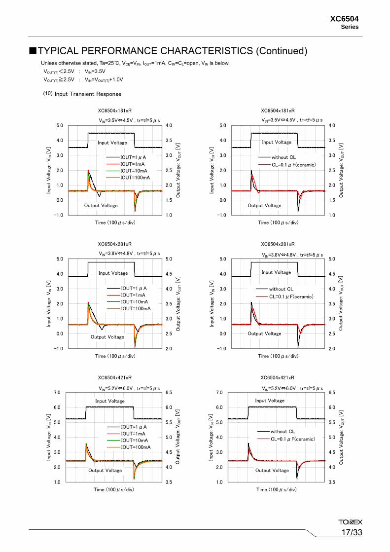
TYPICAL PERFORMANCE CHARACTERISTICS (Continued)
Unless otherwise stated, Ta=25, VCE=VIN, IOUT=1mA, CIN=CL=open, VIN is below. VOUT(T)<2.5V : VIN=3.5V VOUT(T)≧2.5V : VIN=VOUT(T)+1.0V
(9)
(10)
17/33
XC6504Series
(9) Input Transient Response
XC6504x181xR
-1.0
0.0
1.0
2.0
3.0
4.0
5.0
Time (100μs/div)
Inpu
t V
oltag
e: V
IN [
V]
1.0
1.5
2.0
2.5
3.0
3.5
4.0
Outp
ut
Voltag
e: V
OU
T [
V]
IOUT=1μA
IOUT=1mA
IOUT=10mA
IOUT=100mA
VIN=3.5V⇔4.5V , tr=tf=5μs
Input Voltage
Output Voltage
XC6504x181xR
-1.0
0.0
1.0
2.0
3.0
4.0
5.0
Time (100μs/div)
Inpu
t V
oltag
e: V
IN [
V]
1.0
1.5
2.0
2.5
3.0
3.5
4.0
Outp
ut
Voltag
e: V
OU
T [
V]
without CL
CL=0.1μF(ceramic)
VIN=3.5V⇔4.5V , tr=tf=5μs
Input Voltage
Output Voltage
XC6504x281xR
-1.0
0.0
1.0
2.0
3.0
4.0
5.0
Time (100μs/div)
Inpu
t V
oltag
e: V
IN [
V]
2.0
2.5
3.0
3.5
4.0
4.5
5.0
Outp
ut
Voltag
e: V
OU
T [
V]
IOUT=1μA
IOUT=1mA
IOUT=10mA
IOUT=100mA
VIN=3.8V⇔4.8V , tr=tf=5μs
Input Voltage
Output Voltage
XC6504x281xR
-1.0
0.0
1.0
2.0
3.0
4.0
5.0
Time (100μs/div)
Inpu
t V
oltag
e: V
IN [
V]
2.0
2.5
3.0
3.5
4.0
4.5
5.0
Outp
ut
Voltag
e: V
OU
T [
V]
without CL
CL=0.1μF(ceramic)
VIN=3.8V⇔4.8V , tr=tf=5μs
Input Voltage
Output Voltage
XC6504x421xR
1.0
2.0
3.0
4.0
5.0
6.0
7.0
Time (100μs/div)
Inpu
t V
oltag
e: V
IN [
V]
3.5
4.0
4.5
5.0
5.5
6.0
6.5
Outp
ut
Voltag
e: V
OU
T [
V]
IOUT=1μA
IOUT=1mA
IOUT=10mA
IOUT=100mA
VIN=5.2V⇔6.0V , tr=tf=5μs
Input Voltage
Output Voltage
XC6504x421xR
1.0
2.0
3.0
4.0
5.0
6.0
7.0
Time (100μs/div)
Inpu
t V
oltag
e: V
IN [
V]
3.5
4.0
4.5
5.0
5.5
6.0
6.5
Outp
ut
Voltag
e: V
OU
T [
V]
without CL
CL=0.1μF(ceramic)
VIN=5.2V⇔6.0V , tr=tf=5μs
Input Voltage
Output Voltage
TYPICAL PERFORMANCE CHARACTERISTICS (Continued)
Unless otherwise stated, Ta=25, VCE=VIN, IOUT=1mA, CIN=CL=open, VIN is below. VOUT(T)<2.5V : VIN=3.5V VOUT(T)≧2.5V : VIN=VOUT(T)+1.0V
(10)
18/33
XC6504 Series
(10) Load Transient Response
XC6504x121xR
-2
-1
0
1
2
3
Time (200μs/div)
Outp
ut
Voltag
e: V
OU
T [
V]
0
10
20
30
40
50
Outp
ut
Curr
ent: I
OU
T [
mA
]
IOUT=1μA⇔10mA , tr=tf=5μs
Output Voltage
Output Current
XC6504x121xR
-2
-1
0
1
2
3
Time (200μs/div)O
utp
ut
Voltag
e: V
OU
T [
V]
0
30
60
90
120
150
Outp
ut
Curr
ent: I
OU
T [
mA
]
IOUT=10mA⇔30mA , tr=tf=5μs
Output Voltage
Output Current
XC6504x121xR
-2
-1
0
1
2
3
Time (200μs/div)
Outp
ut
Voltag
e: V
OU
T [
V]
0
10
20
30
40
50
Outp
ut
Curr
ent: I
OU
T [
mA
]
IOUT=1mA⇔10mA , tr=tf=5μs
Output Voltage
Output Current
XC6504x121xR
-2
-1
0
1
2
3
Time (200μs/div)
Outp
ut
Voltag
e: V
OU
T [
V]
0
10
20
30
40
50
Outp
ut
Curr
ent: I
OU
T [
mA
]
without CL
CL=0.1μF
CL=1.0μF
IOUT=1mA⇔10mA , tr=tf=5μs
Output Voltage
Output Current
XC6504x181xR
-2
-1
0
1
2
3
Time (200μs/div)
Outp
ut
Voltag
e: V
OU
T [
V]
0
10
20
30
40
50
Outp
ut
Curr
ent: I
OU
T [
mA
]
IOUT=1μA⇔10mA , tr=tf=5μs
Output Voltage
Output Current
XC6504x181xR
-2
-1
0
1
2
3
Time (200μs/div)
Outp
ut
Voltag
e: V
OU
T [
V]
0
30
60
90
120
150
Outp
ut
Curr
ent: I
OU
T [
mA
]
IOUT=10mA⇔30mA , tr=tf=5μs
Output Voltage
Output Current
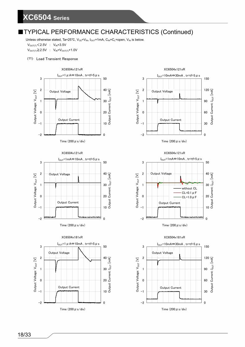
TYPICAL PERFORMANCE CHARACTERISTICS (Continued)
Unless otherwise stated, Ta=25, VCE=VIN, IOUT=1mA, CIN=CL=open, VIN is below. VOUT(T)<2.5V : VIN=3.5V VOUT(T)≧2.5V : VIN=VOUT(T)+1.0V
(11)
19/33
XC6504Series
(10) Load Transient Response
XC6504x181xR
-2
-1
0
1
2
3
Time (200μs/div)
Outp
ut
Voltag
e: V
OU
T [
V]
0
10
20
30
40
50
Outp
ut
Curr
ent: I
OU
T [
mA
]
IOUT=1mA⇔10mA , tr=tf=5μs
Output Voltage
Output Current
XC6504x181xR
-2
-1
0
1
2
3
Time (200μs/div)
Outp
ut
Voltag
e: V
OU
T [
V]
0
10
20
30
40
50
Outp
ut
Curr
ent: I
OU
T [
mA
]
without CL
CL=0.1μF
CL=1.0μF
IOUT=1mA⇔10mA , tr=tf=5μs
Output Voltage
Output Current
XC6504x281xR
-1
0
1
2
3
4
Time (200μs/div)
Outp
ut
Voltag
e: V
OU
T [
V]
0
30
60
90
120
150
Outp
ut
Curr
ent: I
OU
T [
mA
]
IOUT=10mA⇔30mA , tr=tf=5μs
Output Voltage
Output Current
XC6504x281xR
-1
0
1
2
3
4
Time (200μs/div)
Outp
ut
Voltag
e: V
OU
T [
V]
0
10
20
30
40
50
Outp
ut
Curr
ent: I
OU
T [
mA
]
IOUT=1μA⇔10mA , tr=tf=5μs
Output Voltage
Output Current
XC6504x281xR
-1
0
1
2
3
4
Time (200μs/div)
Outp
ut
Voltag
e: V
OU
T [
V]
0
10
20
30
40
50
Outp
ut
Curr
ent: I
OU
T [
mA
]
IOUT=1mA⇔10mA , tr=tf=5μs
Output Voltage
Output Current
XC6504x281xR
-1
0
1
2
3
4
Time (200μs/div)
Outp
ut
Voltag
e: V
OU
T [
V]
0
10
20
30
40
50
Outp
ut
Curr
ent: I
OU
T [
mA
]
without CL
CL=0.1μF
CL=1.0μF
IOUT=1mA⇔10mA , tr=tf=5μs
Output Voltage
Output Current
TYPICAL PERFORMANCE CHARACTERISTICS (Continued)
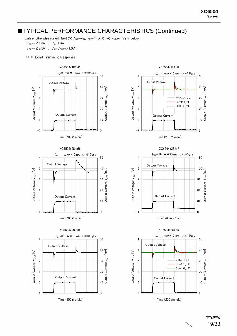
Unless otherwise stated, Ta=25, VCE=VIN, IOUT=1mA, CIN=CL=open, VIN is below. VOUT(T)<2.5V : VIN=3.5V VOUT(T)≧2.5V : VIN=VOUT(T)+1.0V
(11)
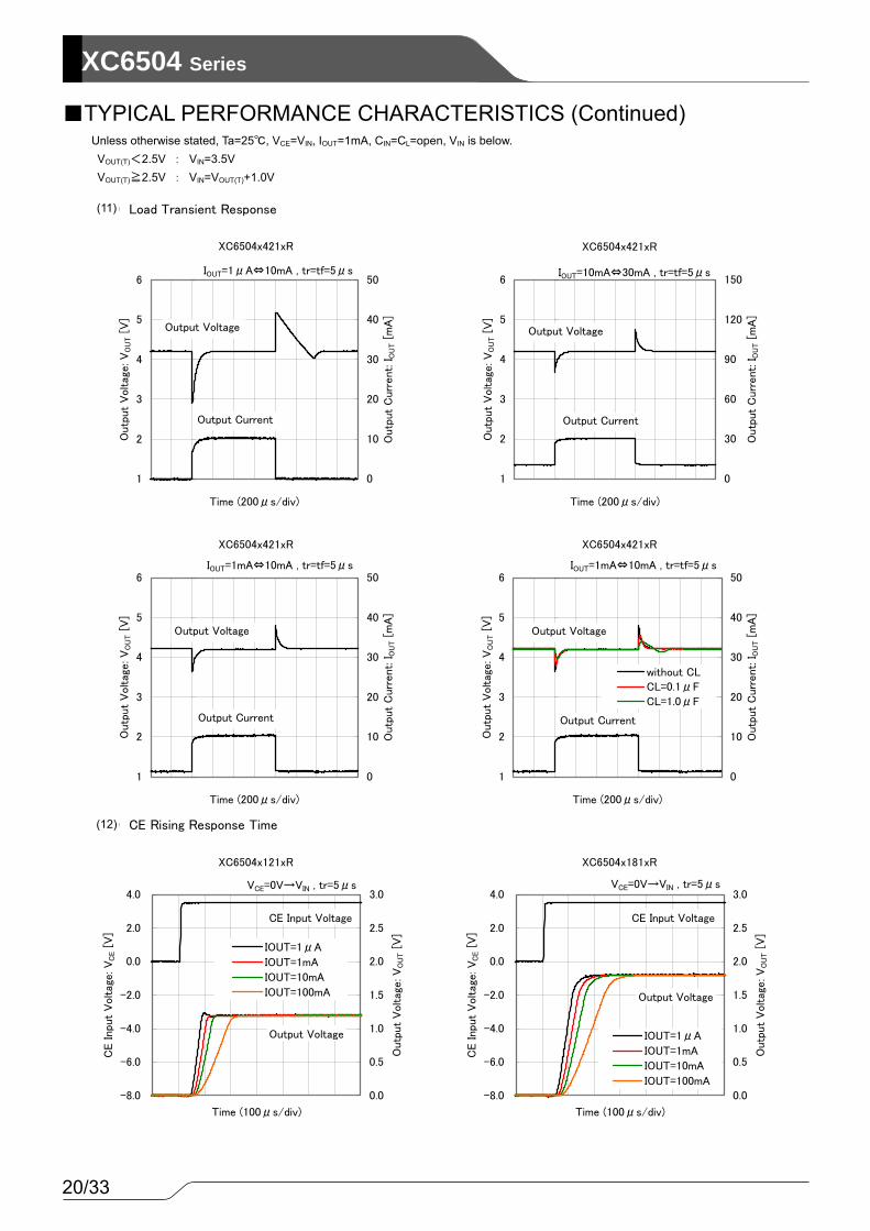
20/33
XC6504 Series
(10) Load Transient Response
(11) CE Rising Response Time
XC6504x421xR
1
2
3
4
5
6
Time (200μs/div)
Outp
ut
Voltag
e: V
OU
T [
V]
0
30
60
90
120
150
Outp
ut
Curr
ent: I
OU
T [
mA
]
IOUT=10mA⇔30mA , tr=tf=5μs
Output Voltage
Output Current
XC6504x421xR
1
2
3
4
5
6
Time (200μs/div)
Outp
ut
Voltag
e: V
OU
T [
V]
0
10
20
30
40
50
Outp
ut
Curr
ent: I
OU
T [
mA
]
IOUT=1mA⇔10mA , tr=tf=5μs
Output Voltage
Output Current
XC6504x421xR
1
2
3
4
5
6
Time (200μs/div)
Outp
ut
Voltag
e: V
OU
T [
V]
0
10
20
30
40
50
Outp
ut
Curr
ent: I
OU
T [
mA
]
IOUT=1μA⇔10mA , tr=tf=5μs
Output Voltage
Output Current
XC6504x421xR
1
2
3
4
5
6
Time (200μs/div)
Outp
ut
Voltag
e: V
OU
T [
V]
0
10
20
30
40
50
Outp
ut
Curr
ent: I
OU
T [
mA
]
without CLCL=0.1μF
CL=1.0μF
IOUT=1mA⇔10mA , tr=tf=5μs
Output Voltage
Output Current
XC6504x121xR
-8.0
-6.0
-4.0
-2.0
0.0
2.0
4.0
Time (100μs/div)
CE Inpu
t V
oltag
e: V
CE [
V]
0.0
0.5
1.0
1.5
2.0
2.5
3.0
Outp
ut
Voltag
e: V
OU
T [
V]
IOUT=1μA
IOUT=1mA
IOUT=10mA
IOUT=100mA
VCE=0V→VIN , tr=5μs
CE Input Voltage
Output Voltage
XC6504x181xR
-8.0
-6.0
-4.0
-2.0
0.0
2.0
4.0
Time (100μs/div)
CE Inpu
t V
oltag
e: V
CE [
V]
0.0
0.5
1.0
1.5
2.0
2.5
3.0
Outp
ut
Voltag
e: V
OU
T [
V]
IOUT=1μA
IOUT=1mA
IOUT=10mA
IOUT=100mA
VCE=0V→VIN , tr=5μs
CE Input Voltage
Output Voltage
TYPICAL PERFORMANCE CHARACTERISTICS (Continued)
Unless otherwise stated, Ta=25, VCE=VIN, IOUT=1mA, CIN=CL=open, VIN is below. VOUT(T)<2.5V : VIN=3.5V VOUT(T)≧2.5V : VIN=VOUT(T)+1.0V
(11)
(12)
21/33
XC6504Series
(11) CE Rising Response Time
(12) Power Supply Rejection Ratio
XC6504x281xR
-6.0
-4.0
-2.0
0.0
2.0
4.0
6.0
Time (100μs/div)
CE Inpu
t V
oltag
e: V
CE [
V]
0.0
1.0
2.0
3.0
4.0
5.0
6.0
Outp
ut
Voltag
e: V
OU
T [
V]
IOUT=1μA
IOUT=1mA
IOUT=10mA
IOUT=100mA
VCE=0V→VIN , tr=5μs
Output Voltage
CE Input Voltage
XC6504x421xR
-6.0
-4.0
-2.0
0.0
2.0
4.0
6.0
Time (100μs/div)
CE Inpu
t V
oltag
e: V
CE [
V]
0.0
1.0
2.0
3.0
4.0
5.0
6.0
Outp
ut
Voltag
e: V
OU
T [
V]
IOUT=1μA
IOUT=1mA
IOUT=10mA
IOUT=100mA
VCE=0V→VIN , tr=5μs
Output Voltage
CE Input Voltage
XC6504x121xR
0
10
20
30
40
50
60
70
80
90
100
10 100 1k 10k 100k 1M
Frequency: f [Hz]
Pow
er
Supp
ly R
eje
ction R
atio
:P
SR
R [
dB]
IOUT=1μA
IOUT=1mA
IOUT=10mA
IOUT=100mA
VIN=3.5V+0.5VP-PAC
XC6504x121xR
0
10
20
30
40
50
60
70
80
90
100
10 100 1k 10k 100k 1M
Frequency: f [Hz]
Pow
er
Supp
ly R
eje
ction R
atio
:P
SR
R [
dB]
without CL
CL=0.1μF(ceramic)
CL=1.0μF(ceramic)
VIN=3.5V+0.5VP-PAC
XC6504x181xR
0
10
20
30
40
50
60
70
80
90
100
10 100 1k 10k 100k 1M
Frequency: f [Hz]
Pow
er
Supp
ly R
eje
ction R
atio
:P
SR
R [
dB]
IOUT=1μA
IOUT=1mA
IOUT=10mA
IOUT=100mA
VIN=3.5V+0.5VP-PAC
XC6504x181xR
0
10
20
30
40
50
60
70
80
90
100
10 100 1k 10k 100k 1M
Frequency: f [Hz]
Pow
er
Supp
ly R
eje
ction R
atio
:P
SR
R [
dB]
without CL
CL=0.1μF(ceramic)
CL=1.0μF(ceramic)
VIN=3.5V+0.5VP-PAC
TYPICAL PERFORMANCE CHARACTERISTICS (Continued)
Unless otherwise stated, Ta=25, VCE=VIN, IOUT=1mA, CIN=CL=open, VIN is below. VOUT(T)<2.5V : VIN=3.5V VOUT(T)≧2.5V : VIN=VOUT(T)+1.0V
(12)
(13)
22/33
XC6504 Series
(12) Power Supply Rejection Ratio
XC6504x281xR
0
10
20
30
40
50
60
70
80
90
100
10 100 1k 10k 100k 1M
Frequency: f [Hz]
Pow
er
Supp
ly R
eje
ction R
atio
:P
SR
R [
dB]
IOUT=1μA
IOUT=1mA
IOUT=10mA
IOUT=100mA
VIN=3.8V+0.5VP-PAC
XC6504x281xR
0
10
20
30
40
50
60
70
80
90
100
10 100 1k 10k 100k 1M
Frequency: f [Hz]
Pow
er
Supp
ly R
eje
ction R
atio
:P
SR
R [
dB]
without CL
CL=0.1μF(ceramic)
CL=1.0μF(ceramic)
VIN=3.8V+0.5VP-PAC
XC6504x421xR
0
10
20
30
40
50
60
70
80
90
100
10 100 1k 10k 100k 1M
Frequency: f [Hz]
Pow
er
Supp
ly R
eje
ction R
atio
:P
SR
R [
dB]
IOUT=1μA
IOUT=1mA
IOUT=10mA
IOUT=100mA
VIN=5.2V+0.5VP-PAC
XC6504x421xR
0
10
20
30
40
50
60
70
80
90
100
10 100 1k 10k 100k 1M
Frequency: f [Hz]
Pow
er
Supp
ly R
eje
ction R
atio
:P
SR
R [
dB]
without CL
CL=0.1μF(ceramic)
CL=1.0μF(ceramic)
VIN=5.2V+0.5VP-PAC
TYPICAL PERFORMANCE CHARACTERISTICS (Continued)
Unless otherwise stated, Ta=25, VCE=VIN, IOUT=1mA, CIN=CL=open, VIN is below. VOUT(T)<2.5V : VIN=3.5V VOUT(T)≧2.5V : VIN=VOUT(T)+1.0V
(13)
23/33
XC6504Series
PACKAGING INFORMATION
USPQ-4B04 Reference Pattern Layout USPQ-4B04 Reference Metal Mask Design
24/33
XC6504 Series
0.75±0.05
1pin INDENT
1 2
4 3
0.18±0.05
(0.4)
USPN-4B02 (unit:mm)
USPN-4B02 参考パターンレイアウト (unit:mm)
0.23 0.23
C0.12
0.14 0.4 0.14
USPN-4B02 参考メタルマスクデザイン (unit:mm)
0.18 0.18
0.115 0.4 0.115
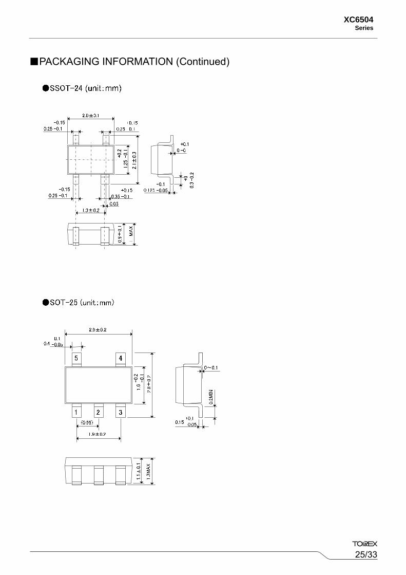
PACKAGING INFORMATION (Continued)
USPN-4B02 Reference Pattern Layout USPN-4B02 Reference Metal Mask Design
25/33
XC6504Series
PACKAGING INFORMATION (Continued)
26/33
XC6504 Series
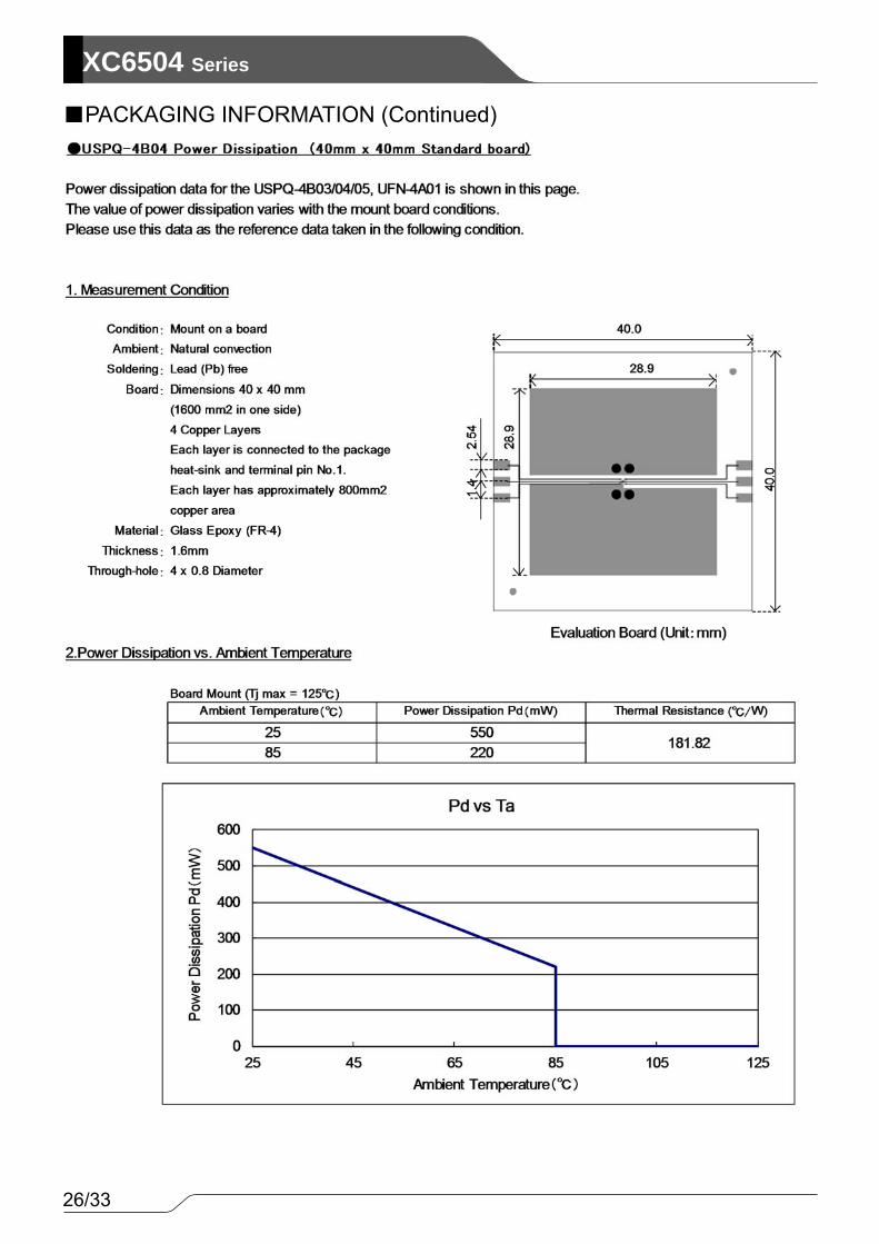
PACKAGING INFORMATION (Continued)
27/33
XC6504Series
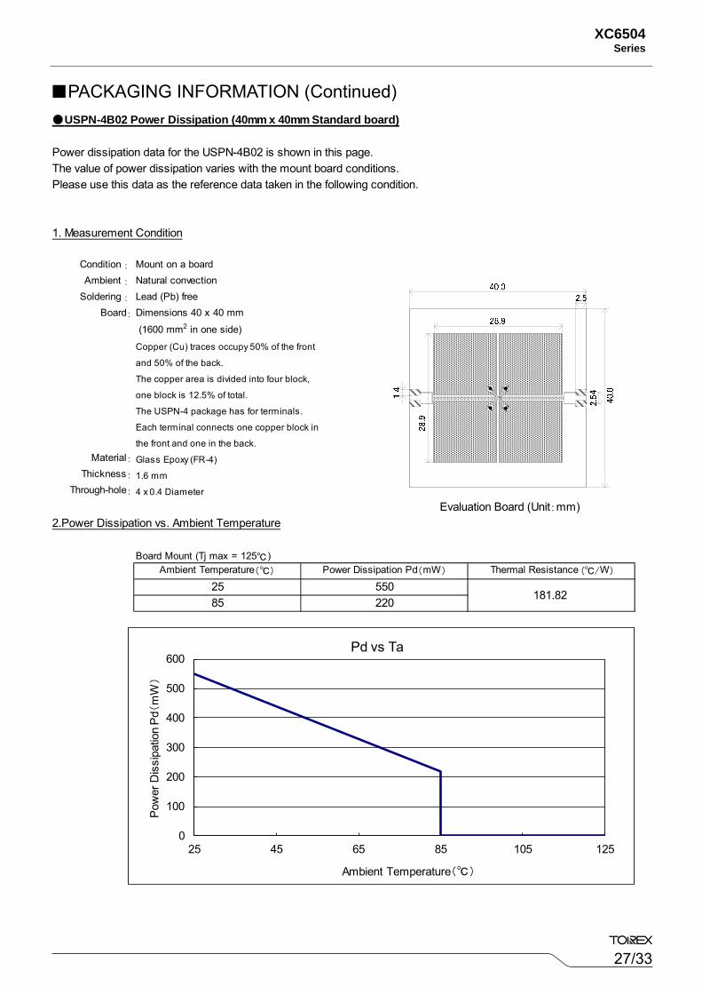
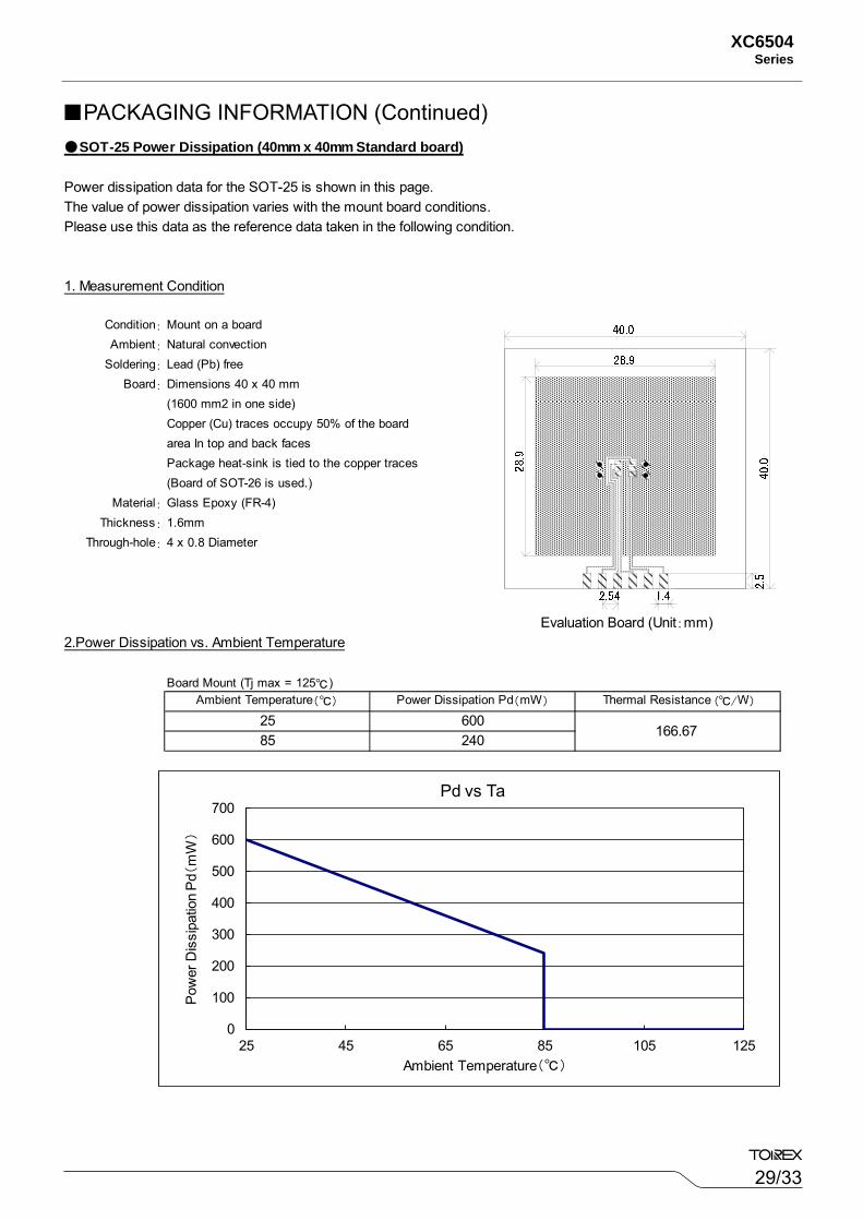
PACKAGING INFORMATION (Continued)
USPN-4B02 Power Dissipation (40mm x 40mm Standard board)
Power dissipation data for the USPN-4B02 is shown in this page.The value of power dissipation varies with the mount board conditions.Please use this data as the reference data taken in the following condition.
1. Measurement Condition
Condition: Mount on a boardAmbient: Natural convection
Soldering: Lead (Pb) freeBoard: Dimensions 40 x 40 mm
(1600 mm2 in one side)
Copper (Cu) traces occupy 50% of the front
and 50% of the back.
The copper area is divided into four block,
one block is 12.5% of total.
The USPN-4 package has for terminals.
Each terminal connects one copper block in
the front and one in the back.Material: Glass Epoxy (FR-4)
Thickness: 1.6 mmThrough-hole: 4 x 0.4 Diameter
Evaluation Board (Unit:mm)2.Power Dissipation vs. Ambient Temperature
Board Mount (Tj max = 125)Ambient Temperature() Power Dissipation Pd(mW) Thermal Resistance (/W)
25 550181.8285 220
0
100
200
300
400
500
600
25 45 65 85 105 125
Pow
er D
issi
patio
n P
d(m
W)
Ambient Temperature()
Pd vs Ta
28/33
XC6504 Series
PACKAGING INFORMATION (Continued)
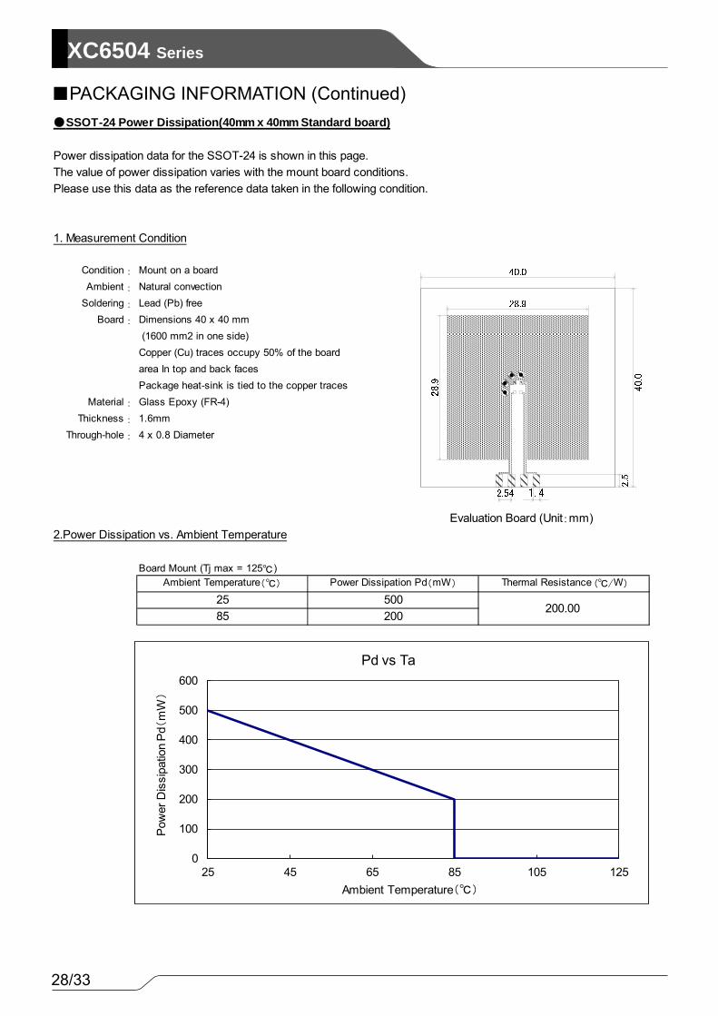
SSOT-24 Power Dissipation(40mm x 40mm Standard board)
Power dissipation data for the SSOT-24 is shown in this page.The value of power dissipation varies with the mount board conditions.Please use this data as the reference data taken in the following condition.
1. Measurement Condition
Condition: Mount on a boardAmbient: Natural convection
Soldering: Lead (Pb) freeBoard: Dimensions 40 x 40 mm
(1600 mm2 in one side) Copper (Cu) traces occupy 50% of the board area In top and back facesPackage heat-sink is tied to the copper traces
Material: Glass Epoxy (FR-4) Thickness: 1.6mm
Through-hole: 4 x 0.8 Diameter
Evaluation Board (Unit:mm)2.Power Dissipation vs. Ambient Temperature
Board Mount (Tj max = 125)Ambient Temperature() Power Dissipation Pd(mW) Thermal Resistance (/W)
25 500200.0085 200
0
100
200
300
400
500
600
25 45 65 85 105 125
Pow
er D
issi
patio
n P
d(m
W)
Ambient Temperature()
Pd vs Ta
29/33
XC6504Series
PACKAGING INFORMATION (Continued)
SOT-25 Power Dissipation (40mm x 40mm Standard board)
Power dissipation data for the SOT-25 is shown in this page.The value of power dissipation varies with the mount board conditions.Please use this data as the reference data taken in the following condition.
1. Measurement Condition
Condition: Mount on a boardAmbient: Natural convection
Soldering: Lead (Pb) freeBoard: Dimensions 40 x 40 mm
(1600 mm2 in one side) Copper (Cu) traces occupy 50% of the boardarea In top and back facesPackage heat-sink is tied to the copper traces(Board of SOT-26 is used.)
Material: Glass Epoxy (FR-4) Thickness: 1.6mm
Through-hole: 4 x 0.8 Diameter
Evaluation Board (Unit:mm)2.Power Dissipation vs. Ambient Temperature
Board Mount (Tj max = 125)Ambient Temperature() Power Dissipation Pd(mW) Thermal Resistance (/W)
25 600166.6785 240
0
100
200
300
400
500
600
700
25 45 65 85 105 125
Pow
er D
issi
patio
n P
d(m
W)
Ambient Temperature()
Pd vs Ta
30/33
XC6504 Series
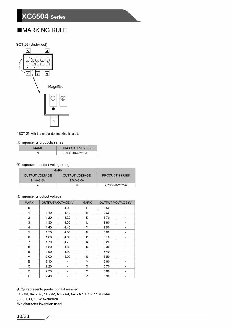
MARKING RULE
* SOT-25 with the under-dot marking is used.
① represents products series
② represents output voltage range
③ represents output voltage
④,⑤ represents production lot number 01~09, 0A~0Z, 11~9Z, A1~A9, AA~AZ, B1~ZZ in order. (G, I, J, O, Q, W excluded) *No character inversion used.
MARK PRODUCT SERIES
9 XC6504A*****-G
MARK
PRODUCT SERIES OUTPUT VOLTAGE 1.1V~3.9V
OUTPUT VOLTAGE 4.0V~5.0V
A B XC6504A*****-G
MARK OUTPUT VOLTAGE (V) MARK OUTPUT VOLTAGE (V)
0 - 4.00 F 2.50 - 1 1.10 4.10 H 2.60 - 2 1.20 4.20 K 2.70 - 3 1.30 4.30 L 2.80 - 4 1.40 4.40 M 2.90 - 5 1.50 4.50 N 3.00 - 6 1.60 4.60 P 3.10 - 7 1.70 4.70 R 3.20 - 8 1.80 4.80 S 3.30 - 9 1.90 4.90 T 3.40 - A 2.00 5.00 U 3.50 - B 2.10 - V 3.60 - C 2.20 - X 3.70 - D 2.30 - Y 3.80 - E 2.40 - Z 3.90 -
SOT-25 (Under-dot)
Magnified
31/33
XC6504Series
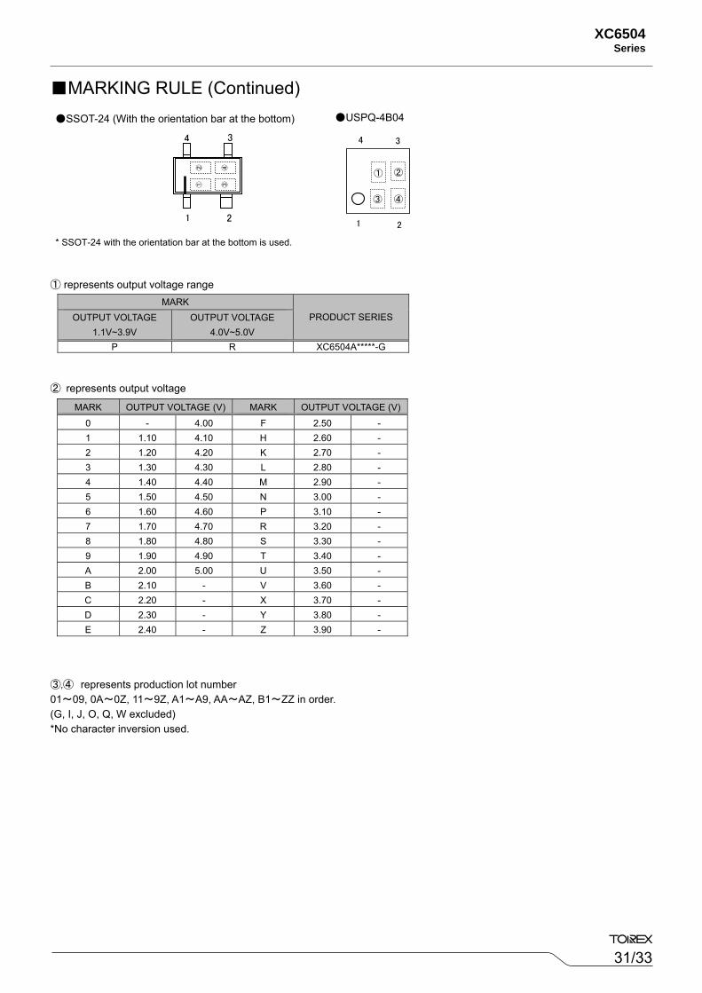
MARKING RULE (Continued)
① represents output voltage range
② represents output voltage
③,④ represents production lot number 01~09, 0A~0Z, 11~9Z, A1~A9, AA~AZ, B1~ZZ in order. (G, I, J, O, Q, W excluded) *No character inversion used.
MARK
PRODUCT SERIES OUTPUT VOLTAGE 1.1V~3.9V
OUTPUT VOLTAGE 4.0V~5.0V
P R XC6504A*****-G
MARK OUTPUT VOLTAGE (V) MARK OUTPUT VOLTAGE (V)
0 - 4.00 F 2.50 - 1 1.10 4.10 H 2.60 - 2 1.20 4.20 K 2.70 - 3 1.30 4.30 L 2.80 - 4 1.40 4.40 M 2.90 - 5 1.50 4.50 N 3.00 - 6 1.60 4.60 P 3.10 - 7 1.70 4.70 R 3.20 - 8 1.80 4.80 S 3.30 - 9 1.90 4.90 T 3.40 - A 2.00 5.00 U 3.50 - B 2.10 - V 3.60 - C 2.20 - X 3.70 - D 2.30 - Y 3.80 - E 2.40 - Z 3.90 -
SSOT-24 (With the orientation bar at the bottom)
④1 2
34
③
②①
* SSOT-24 with the orientation bar at the bottom is used.
USPQ-4B04
③ ④
① ②
1 2
4 3
32/33
XC6504 Series
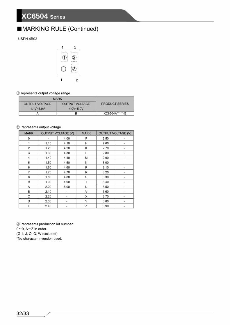
MARKING RULE (Continued)
① represents output voltage range
② represents output voltage
③ represents production lot number 0~9, A~Z in order. (G, I, J, O, Q, W excluded) *No character inversion used.
MARK
PRODUCT SERIES OUTPUT VOLTAGE 1.1V~3.9V
OUTPUT VOLTAGE 4.0V~5.0V
A B XC6504A*****-G
MARK OUTPUT VOLTAGE (V) MARK OUTPUT VOLTAGE (V)
0 - 4.00 F 2.50 - 1 1.10 4.10 H 2.60 - 2 1.20 4.20 K 2.70 - 3 1.30 4.30 L 2.80 - 4 1.40 4.40 M 2.90 - 5 1.50 4.50 N 3.00 - 6 1.60 4.60 P 3.10 - 7 1.70 4.70 R 3.20 - 8 1.80 4.80 S 3.30 - 9 1.90 4.90 T 3.40 - A 2.00 5.00 U 3.50 - B 2.10 - V 3.60 - C 2.20 - X 3.70 - D 2.30 - Y 3.80 - E 2.40 - Z 3.90 -
USPN-4B02
③
① ②
1 2
4 3
33/33
XC6504Series
1. The product and product specifications contained herein are subject to change without notice to improve performance characteristics. Consult us, or our representatives before use, to confirm that the information in this datasheet is up to date.
2. The information in this datasheet is intended to illustrate the operation and characteristics of our
products. We neither make warranties or representations with respect to the accuracy or completeness of the information contained in this datasheet nor grant any license to any intellectual property rights of ours or any third party concerning with the information in this datasheet.
3. Applicable export control laws and regulations should be complied and the procedures required by
such laws and regulations should also be followed, when the product or any information contained in this datasheet is exported.
4. The product is neither intended nor warranted for use in equipment of systems which require
extremely high levels of quality and/or reliability and/or a malfunction or failure which may cause loss of human life, bodily injury, serious property damage including but not limited to devices or equipment used in 1) nuclear facilities, 2) aerospace industry, 3) medical facilities, 4) automobile industry and other transportation industry and 5) safety devices and safety equipment to control combustions and explosions. Do not use the product for the above use unless agreed by us in writing in advance.
5. Although we make continuous efforts to improve the quality and reliability of our products;
nevertheless Semiconductors are likely to fail with a certain probability. So in order to prevent personal injury and/or property damage resulting from such failure, customers are required to incorporate adequate safety measures in their designs, such as system fail safes, redundancy and fire prevention features.
6. Our products are not designed to be Radiation-resistant.
7. Please use the product listed in this datasheet within the specified ranges.
8. We assume no responsibility for damage or loss due to abnormal use.
9. All rights reserved. No part of this datasheet may be copied or reproduced unless agreed by Torex
Semiconductor Ltd in writing in advance.
TOREX SEMICONDUCTOR LTD.