LM317M 3-Terminal Adjustable Regulator - Texas … temperature range 0.3 1.5 ADJUST terminal current...
23
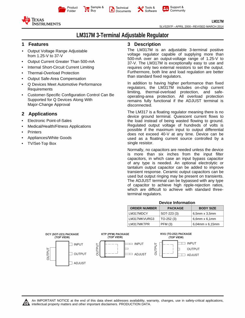
INPUT ADJUST INPUT OUTPUT ADJUST OUTPUT OUTPUT KVU (TO-252) PACKAGE (TOP VIEW) OUTPUT INPUT ADJUST OUTPUT KTP (PFM) PACKAGE (TOP VIEW) DCY (SOT-223) PACKAGE (TOP VIEW) Product Folder Sample & Buy Technical Documents Tools & Software Support & Community LM317M SLVS297P – APRIL 2000 – REVISED MARCH 2014 LM317M 3-Terminal Adjustable Regulator 1 Features 3 Description The LM317M is an adjustable 3-terminal positive 1• Output Voltage Range Adjustable voltage regulator capable of supplying more than from 1.25-V to 37-V 500-mA over an output-voltage range of 1.25-V to • Output Current Greater Than 500-mA 37-V. The LM317M is exceptionally easy to use and • Internal Short-Circuit Current Limiting requires only two external resistors to set the output. Furthermore, both line and load regulation are better • Thermal-Overload Protection than standard fixed regulators. • Output Safe-Area Compensation In addition to having higher performance than fixed • Q Devices Meet Automotive Performance regulators, the LM317M includes on-chip current Requirements limiting, thermal-overload protection, and safe- • Customer-Specific Configuration Control Can Be operating-area protection. All overload protection Supported for Q Devices Along With remains fully functional if the ADJUST terminal is Major-Change Approval disconnected. The LM317 is a floating regulator meaning there is no 2 Applications device ground terminal. Quiescent current flows to • Electronic Point-of-Sales the load instead of being wasted flowing to ground. Regulated output voltage of hundreds of volts is • Medical/Health/Fitness Applications possible if the maximum input to output differential • Printers does not exceed 40-V at any time. Device can be • Appliances/White Goods used as a floating current source controlled by a single resistor. • TV/Set-Top Box Normally, no capacitors are needed unless the device is more than six inches from the input filter capacitors, in which case an input bypass capacitor of any type is needed. An optional electrolytic or tantalum output capacitor can be added to improve transient response. Ceramic output capacitors can be used but output ringing may be present on transients. The ADJUST terminal can be bypassed with any type of capacitor to achieve high ripple-rejection ratios, which are difficult to achieve with standard three- terminal regulators. Device Information ORDER NUMBER PACKAGE BODY SIZE LM317MDCY SOT-223 (3) 6,5mm x 3,5mm LM317MKVURG3 TO-252 (3) 6,6mm x 6,1mm LM317MKTPR PFM (3) 6,04mm x 6,15mm 1 An IMPORTANT NOTICE at the end of this data sheet addresses availability, warranty, changes, use in safety-critical applications, intellectual property matters and other important disclaimers. PRODUCTION DATA.
Transcript of LM317M 3-Terminal Adjustable Regulator - Texas … temperature range 0.3 1.5 ADJUST terminal current...
INPUT
ADJUST
INPUT
OUTPUT
ADJUST
OU
TP
UT
OU
TP
UT
KVU (TO-252) PACKAGE
(TOP VIEW)
OUTPUT
INPUT
ADJUSTOU
TP
UT
KTP (PFM) PACKAGE(TOP VIEW)
DCY (SOT-223) PACKAGE(TOP VIEW)
Product
Folder
Sample &Buy
Technical
Documents
Tools &
Software
Support &Community
LM317MSLVS297P –APRIL 2000–REVISED MARCH 2014
LM317M 3-Terminal Adjustable Regulator1 Features 3 Description
The LM317M is an adjustable 3-terminal positive1• Output Voltage Range Adjustable
voltage regulator capable of supplying more thanfrom 1.25-V to 37-V500-mA over an output-voltage range of 1.25-V to
• Output Current Greater Than 500-mA 37-V. The LM317M is exceptionally easy to use and• Internal Short-Circuit Current Limiting requires only two external resistors to set the output.
Furthermore, both line and load regulation are better• Thermal-Overload Protectionthan standard fixed regulators.• Output Safe-Area CompensationIn addition to having higher performance than fixed• Q Devices Meet Automotive Performanceregulators, the LM317M includes on-chip currentRequirementslimiting, thermal-overload protection, and safe-
• Customer-Specific Configuration Control Can Be operating-area protection. All overload protectionSupported for Q Devices Along With remains fully functional if the ADJUST terminal isMajor-Change Approval disconnected.
The LM317 is a floating regulator meaning there is no2 Applications device ground terminal. Quiescent current flows to• Electronic Point-of-Sales the load instead of being wasted flowing to ground.
Regulated output voltage of hundreds of volts is• Medical/Health/Fitness Applicationspossible if the maximum input to output differential• Printers does not exceed 40-V at any time. Device can be
• Appliances/White Goods used as a floating current source controlled by asingle resistor.• TV/Set-Top BoxNormally, no capacitors are needed unless the deviceis more than six inches from the input filtercapacitors, in which case an input bypass capacitorof any type is needed. An optional electrolytic ortantalum output capacitor can be added to improvetransient response. Ceramic output capacitors can beused but output ringing may be present on transients.The ADJUST terminal can be bypassed with any typeof capacitor to achieve high ripple-rejection ratios,which are difficult to achieve with standard three-terminal regulators.
Device InformationORDER NUMBER PACKAGE BODY SIZE
LM317MDCY SOT-223 (3) 6,5mm x 3,5mmLM317MKVURG3 TO-252 (3) 6,6mm x 6,1mmLM317MKTPR PFM (3) 6,04mm x 6,15mm
1
An IMPORTANT NOTICE at the end of this data sheet addresses availability, warranty, changes, use in safety-critical applications,intellectual property matters and other important disclaimers. PRODUCTION DATA.
LM317MSLVS297P –APRIL 2000–REVISED MARCH 2014 www.ti.com
Table of Contents7.3 Feature Description................................................... 71 Features .................................................................. 17.4 Device Functional Modes.......................................... 82 Applications ........................................................... 1
8 Applications and Implementation ........................ 93 Description ............................................................. 18.1 Application Information.............................................. 94 Revision History..................................................... 28.2 Typical Application .................................................... 95 Terminal Configuration and Functions................ 3
9 Power Supply Recommendations ...................... 116 Specifications......................................................... 310 Layout................................................................... 116.1 Absolute Maximum Ratings ..................................... 3
10.1 Layout Guidelines ................................................. 116.2 Handling Ratings....................................................... 310.2 Layout Example .................................................... 116.3 Recommended Operating Conditions....................... 3
11 Device and Documentation Support ................. 126.4 Thermal Information .................................................. 411.1 Trademarks ........................................................... 126.5 Electrical Characteristics........................................... 411.2 Electrostatic Discharge Caution............................ 126.6 Typical Characteristics .............................................. 511.3 Glossary ................................................................ 127 Detailed Description .............................................. 7
12 Mechanical, Packaging, and Orderable7.1 Overview ................................................................... 7Information ........................................................... 127.2 Functional Block Diagram ......................................... 7
4 Revision History
Changes from Revision O (July 2006) to Revision P Page
• Removed Ordering Information Table ................................................................................................................................... 1• Clarified TJ package field ....................................................................................................................................................... 3
2 Submit Documentation Feedback Copyright © 2000–2014, Texas Instruments Incorporated
Product Folder Links: LM317M
INPUT
ADJUST
INPUT
OUTPUT
ADJUST
OU
TP
UT
OU
TP
UT
KVU (TO-252) PACKAGE
(TOP VIEW)
OUTPUT
INPUT
ADJUSTOU
TP
UT
KTP (PFM) PACKAGE(TOP VIEW)
DCY (SOT-223) PACKAGE(TOP VIEW)
LM317Mwww.ti.com SLVS297P –APRIL 2000–REVISED MARCH 2014
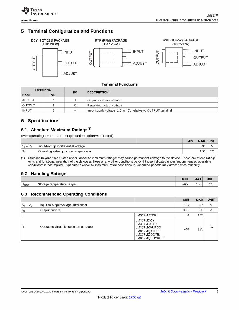
5 Terminal Configuration and Functions
Terminal FunctionsTERMINAL
I/O DESCRIPTIONNAME NO.ADJUST 1 I Output feedback voltageOUTPUT 2 O Regulated output voltageINPUT 3 – Input supply voltage, 2.5 to 40V relative to OUTPUT terminal
6 Specifications
6.1 Absolute Maximum Ratings (1)
over operating temperature range (unless otherwise noted)MIN MAX UNIT
VI – VO Input-to-output differential voltage 40 VTJ Operating virtual junction temperature 150 °C
(1) Stresses beyond those listed under "absolute maximum ratings" may cause permanent damage to the device. These are stress ratingsonly, and functional operation of the device at these or any other conditions beyond those indicated under "recommended operatingconditions" is not implied. Exposure to absolute-maximum-rated conditions for extended periods may affect device reliability.
6.2 Handling RatingsMIN MAX UNIT
TSTG Storage temperature range –65 150 °C
6.3 Recommended Operating ConditionsMIN MAX UNIT
VI – VO Input-to-output voltage differential 2.5 37 VIO Output current 0.01 0.5 A
LM317MKTPR 0 125LM317MDCY,LM317MDCYR,
TJ Operating virtual junction temperature °CLM317MKVURG3, –40 125LM317MQKTPR,LM317MQDCYR,LM317MQDCYRG3
Copyright © 2000–2014, Texas Instruments Incorporated Submit Documentation Feedback 3
Product Folder Links: LM317M
LM317MSLVS297P –APRIL 2000–REVISED MARCH 2014 www.ti.com
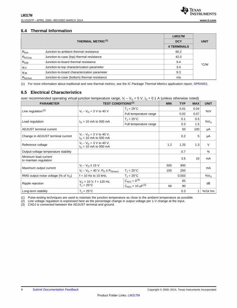
6.4 Thermal InformationLM317M
THERMAL METRIC (1) DCY UNIT4 TERMINALS
RθJA Junction-to-ambient thermal resistance 60.2RθJCtop Junction-to-case (top) thermal resistance 42.0RθJB Junction-to-board thermal resistance 9.4
°C/WψJT Junction-to-top characterization parameter 3.4ψJB Junction-to-board characterization parameter 9.3RθJCbot Junction-to-case (bottom) thermal resistance n/a
(1) For more information about traditional and new thermal metrics, see the IC Package Thermal Metrics application report, SPRA953.
6.5 Electrical Characteristicsover recommended operating virtual-junction temperature range, VI – VO = 5 V, IO = 0.1 A (unless otherwise noted)
PARAMETER TEST CONDITIONS (1) MIN TYP MAX UNITTJ = 25°C 0.01 0.04
Line regulation (2) VI – VO = 3 V to 40 V %/VFull temperature range 0.02 0.07TJ = 25°C 0.1 0.5
Load regulation IO = 10 mA to 500 mA %VOFull temperature range 0.3 1.5ADJUST terminal current 50 100 μA
VI – VO = 3 V to 40 V,Change in ADJUST terminal current 0.2 5 μAIO = 10 mA to 500 mAVI – VO = 3 V to 40 V,Reference voltage 1.2 1.25 1.3 VIO = 10 mA to 500 mA
Output-voltage temperature stability 0.7 %Minimum load current 3.5 10 mAto maintain regulation
VI – VO ≤ 15 V 500 900Maximum output current mA
VI – VO = 40 V, PD ≤ PD(max), TJ = 25°C 150 250RMS output noise voltage (% of VO) f = 10 Hz to 10 kHz, TJ = 25°C 0.003 %VO
CADJ = 0 (3) 65VO = 10 V, f = 120 Hz,Ripple rejection dBTJ = 25°C CADJ = 10 μF (3) 66 80Long-term stability TJ = 25°C 0.3 1 %/1k hrs
(1) Pulse-testing techniques are used to maintain the junction temperature as close to the ambient temperature as possible.(2) Line voltage regulation is expressed here as the percentage change in output voltage per 1-V change at the input.(3) CADJ is connected between the ADJUST terminal and ground.
4 Submit Documentation Feedback Copyright © 2000–2014, Texas Instruments Incorporated
Product Folder Links: LM317M
0 5 10 15 20
VI − VO − Input-Output Differential − V
7
6
5
4
3
2
1
0
Min
imum
Ope
ratin
g C
urre
nt −
mA TJ = 125°C
25 30 35 40
TJ = 25°C
8
0 5 10 15
1.00
0.80
0.60
0.40
0.20
0.0020 25 30 35 40
TJ = 125°C
TJ = 25°C
V – V – Input-Output Differential – VI O
I–
Out
put C
urre
nt –
AO
0 25 50
TJ − Temperature − °C
1.260VI = 4.25 VVO = VrefIL = 10 mA1.255
1.250
1.245
1.240
1.235
1.230
1.225
1.220
Vre
f−
Ref
eren
ce V
olta
ge −
V
75 100 1250 25 50
53
51
49
47
45
43
41
39
37
35
AD
JUS
T T
erm
inal
Cur
rent
−µ
A
IL = 10 mA
IL = 100 mA
TJ − Temperature − °C
55
75 100 125
VI = 6.25 VVO = Vref
0 25 50
TJ − Temperature − °C
∆V
O−
Out
put V
olta
ge C
hang
e −
%
0.20
0.15
0.10
0.05
0.00
−0.05
−0.10
−0.15
−0.20
−0.25
−0.30
−0.35
−0.4075 100 125
VI = 45 VVO = 5 VIL = 10 mA to 100 mA
VI = 10 VVO = 5 VIL = 10 mA to 40 mA
0 25 50 75 100 1250
0.10
0.20
0.30
0.40
0.50
0.60
0.70
0.80
0.90
1.00
TJ − Temperature − °C
∆V
O−
Out
put V
olta
ge C
hang
e −
%
VI = 4.25 V to 41.25 VVO = VrefIL = 10 mA
LM317Mwww.ti.com SLVS297P –APRIL 2000–REVISED MARCH 2014
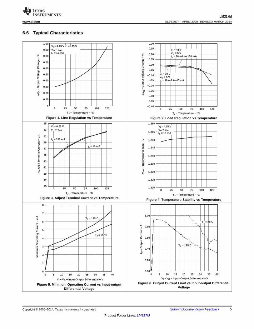
6.6 Typical Characteristics
Figure 1. Line Regulation vs Temperature Figure 2. Load Regulation vs Temperature
Figure 3. Adjust Terminal Current vs Temperature Figure 4. Temperature Stability vs Temperature
Figure 6. Output Current Limit vs Input-output DifferentialFigure 5. Minimum Operating Current vs Input-outputVoltageDifferential Voltage
Copyright © 2000–2014, Texas Instruments Incorporated Submit Documentation Feedback 5
Product Folder Links: LM317M
10 Hz
Frequency
10.00
50 Hz 100 Hz 500 Hz 1 kHz 5 kHz 10 kHz 50 kHz 100 kHz 150 kHz
1.00
0.10
0.01
Out
put I
mpe
danc
e −
Ω
VI = 15 VVO = 10 VIL = 100-mA dc and 10-mA RMS
CADJ = 0 µF
CADJ = 10 µF
10 Hz
Frequency
100
Rip
ple
Rej
ectio
n −
dB
100 Hz 1 kHz
90
80
70
60
50
40
30
20
10
0
VI = 15 Vdc and V ac = 1 VPPVO = 10 VIL = 100 mACL = 1 µFCi = 0.1 µF
CADJ = 0 µF
CADJ = 10 µF
10 kHz 100 kHz 0 25 50
TJ − Temperature − °C
2.5
2
1.5
1
0.5
0
IL = 500 mA
IL = 100 mA
− V
O(V
I) −
Inpu
t-Out
put V
olta
ge D
iffer
entia
l − V
75 100 125
0 25 50
TJ − Temperature − °C
0.004
0.003
0.002
0.001
0.000
VI = 15 VVO = 10 VIL = 50 mABandwidth = 10 Hz to 10 kHz
75 100 125
% V
OO
uput
Noi
se V
olta
ge −
0 25 70
TJ − Temperature − °C
90
85
80
75
70
65
60
55
50
45
Rip
ple
Rej
ectio
n −
dB
VI = 15 Vdc and 1 V PP (120 Hz)VO = 10 VIL = 100 mACL = 1 µFCi = 0.1 µF
85 125
CADJ = 0 µF
CADJ = 10 µF
LM317MSLVS297P –APRIL 2000–REVISED MARCH 2014 www.ti.com
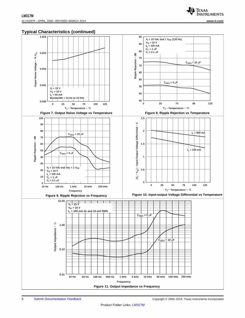
Typical Characteristics (continued)
Figure 7. Output Noise Voltage vs Temperature Figure 8. Ripple Rejection vs Temperature
Figure 10. Input-output Voltage Differential vs TemperatureFigure 9. Ripple Rejection vs Frequency
Figure 11. Output Impedance vs Frequency
6 Submit Documentation Feedback Copyright © 2000–2014, Texas Instruments Incorporated
Product Folder Links: LM317M
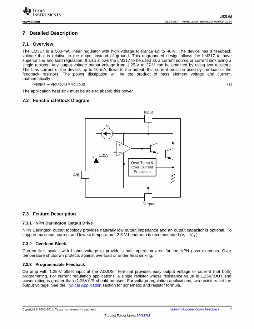
+
Over Temp & Over Current
Protection
Input
Adj.
Output
1.25V
Iadj
LM317Mwww.ti.com SLVS297P –APRIL 2000–REVISED MARCH 2014
7 Detailed Description
7.1 OverviewThe LM317 is a 500-mA linear regulator with high voltage tolerance up to 40-V. The device has a feedbackvoltage that is relative to the output instead of ground. This ungrounded design allows the LM317 to havesuperior line and load regulation. It also allows the LM317 to be used as a current source or current sink using asingle resistor. Any output voltage output voltage from 1.25-V to 37-V can be obtained by using two resistors.The bias current of the device, up to 10-mA, flows to the output; this current must be used by the load or thefeedback resistors. The power dissipation will be the product of pass element voltage and current,mathematically:
(V[input] – V[output]) × I[output] (1)
The application heat sink must be able to absorb this power.
7.2 Functional Block Diagram
7.3 Feature Description
7.3.1 NPN Darlington Output DriveNPN Darlington output topology provides naturally low output impedance and an output capacitor is optional. Tosupport maximum current and lowest temperature, 2.5-V headroom is recommended (VI – VO ).
7.3.2 Overload BlockCurrent limit scales with higher voltage to provide a safe operation area for the NPN pass elements. Overtemperature shutdown protects against overload or under heat sinking.
7.3.3 Programmable FeedbackOp amp with 1.25-V offset input at the ADJUST terminal provides easy output voltage or current (not both)programming. For current regulation applications, a single resistor whose resistance value is 1.25V/IOUT andpower rating is greater than (1.25V)2/R should be used. For voltage regulation applications, two resistors set theoutput voltage. See the Typical Application section for schematic and resistor formula.
Copyright © 2000–2014, Texas Instruments Incorporated Submit Documentation Feedback 7
Product Folder Links: LM317M
LM317MSLVS297P –APRIL 2000–REVISED MARCH 2014 www.ti.com
Feature Description (continued)7.3.4 Current SourcesThe two current sources represent the typical ‘adjust terminal current’ and typical ‘minimum current forregulation'.
7.4 Device Functional Modes
7.4.1 Normal operationThe device OUTPUT terminal will source current necessary to make OUTPUT terminal 1.25-V greater thanADJUST terminal to provide output regulation.
7.4.2 Operation With Low Input VoltageThe device requires up to 2.5-V headroom (Vin-Vout) to operate in regulation. With less headroom, the devicemay drop out and OUTPUT voltage will be INPUT voltage minus drop out voltage.
7.4.3 Operation at Light LoadsThe device passes its bias current to the OUTPUT terminal. The load or feedback must consume this minimumcurrent for regulation or the output may be too high.
7.4.4 Operation In Self ProtectionWhen an overload occurs the device will shut down Darlington NPN output stage or reduce the output current toprevent device damage. The device will automatically reset from the overload. The output may be reduced oralternate between on and off until the overload is removed.
7.4.5 Operation at Light LoadsThe device passes its bias current to the OUTPUT terminal. The load or feedback must consume this minimumcurrent for regulation or the output may be too high.
8 Submit Documentation Feedback Copyright © 2000–2014, Texas Instruments Incorporated
Product Folder Links: LM317M
LM317M
CADJ
R2
Input Output
Adjust
Vref=1.25V
VO
D21N4002
R1
240 ΩIADJ
C
0.1I
μF
VI
D11N4002
C
1.0 FI
μ
LM317Mwww.ti.com SLVS297P –APRIL 2000–REVISED MARCH 2014
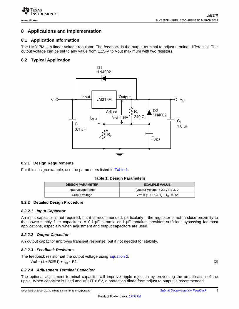
8 Applications and Implementation
8.1 Application InformationThe LM317M is a linear voltage regulator. The feedback is the output terminal to adjust terminal differential. Theoutput voltage can be set to any value from 1.25-V to Vout maximum with two resistors.
8.2 Typical Application
8.2.1 Design RequirementsFor this design example, use the parameters listed in Table 1.
Table 1. Design ParametersDESIGN PARAMETER EXAMPLE VALUE
Input voltage range (Output Voltage + 2.5V) to 37VOutput voltage Vref × (1 + R2/R1) + Iadj × R2
8.2.2 Detailed Design Procedure
8.2.2.1 Input CapacitorAn input capacitor is not required, but it is recommended, particularly if the regulator is not in close proximity tothe power-supply filter capacitors. A 0.1-µF ceramic or 1-µF tantalum provides sufficient bypassing for mostapplications, especially when adjustment and output capacitors are used.
8.2.2.2 Output CapacitorAn output capacitor improves transient response, but it not needed for stability.
8.2.2.3 Feedback ResistorsThe feedback resistor set the output voltage using Equation 2.
Vref × (1 + R2/R1) + Iadj × R2 (2)
8.2.2.4 Adjustment Terminal CapacitorThe optional adjustment terminal capacitor will improve ripple rejection by preventing the amplification of theripple. When capacitor is used and VOUT > 6V, a protection diode from adjust to output is recommended.
Copyright © 2000–2014, Texas Instruments Incorporated Submit Documentation Feedback 9
Product Folder Links: LM317M
−10
Time − µs
−0.2
∆I O
−O
utpu
t Cur
rent
Cha
nge
− A
∆V
O−
Out
put V
olta
ge C
hang
e −
V
−5 0 5 10 15 20 25 30 35
−0.10
0.10.20.30.40.50.6
−4.0
−3.0
−2.0
−1.0
0
1.0
2.0
3.0
4.0
5.0VI = 15 VVO = 10 VIL = 50 mA∆IL = +500 mA
CL = 1 µFCADJ = 10 µF
CL = 0 µFCADJ = 0 µF
−1.0
Time − µs
−0.5 0 0.5 1.0 1.5 2.0 2.5 3.0 3.5 4.0 4.5
1.2
1
0.8
0.6
0.4
0.2
0
−1
−0.8
−0.6
−0.4
−0.2
0
0.2
0.4
0.6
0.8
1
VO = 10 VVI = 15 V, ∆VI = +1 VIL = 50 mATJ = 25°CCL = 0 µFCADJ = 0 µF
∆V
I−
Inpu
t Vol
tage
Cha
nge
− V
∆V
O−
Out
put V
olta
ge C
hang
e −
V
)()1( 21
2 RIR
RVV adjrefo uu
LM317MSLVS297P –APRIL 2000–REVISED MARCH 2014 www.ti.com
8.2.2.5 Protection DiodesIf the input is shorted to ground during a fault condition, protection diode (D1) prevents discharge through theLM317M. If the output is shorted to ground during a fault condition, protection diode (D2) prevents adjust terminalcapacitor discharge through the LM317M.
8.2.2.6 Design Options and ParametersCommon Linear Regulator designs are concerned with the following parameters:
• Input voltage range• Input Capacitor range• Output voltage• Output current rating• Output capacitor range• Input Short Protection• Stability• Ripple Rejection
8.2.2.7 Output VoltageVo is calculated as shown:
(3)
Because Iadj typically is 50-µA, it is negligible in most applications.
8.2.2.8 Ripple RejectionCADJ is used to improve ripple rejection; it prevents amplification of the ripple as the output voltage is adjustedhigher. If CADJ is used, it is best to include protection diodes.
8.2.2.9 Input Short ProtectionIf the input is shorted to ground during a fault condition, protection diodes provide measures to prevent thepossibility of external capacitors discharging through low-impedance paths in the IC. By providing low-impedancedischarge paths for CO and CADJ, respectively, D1 and D2 prevent the capacitors from discharging into the outputof the regulator.
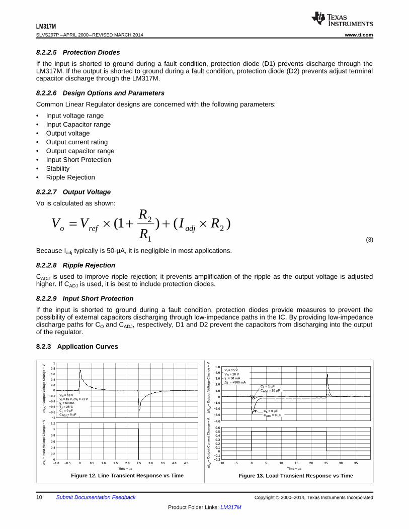
8.2.3 Application Curves
Figure 12. Line Transient Response vs Time Figure 13. Load Transient Response vs Time
10 Submit Documentation Feedback Copyright © 2000–2014, Texas Instruments Incorporated
Product Folder Links: LM317M
R1
OUTPUT
INP
UT
OU
TP
UT
AD
J/G
ND
R2
Cadj
COUT
0.1 Fμ 10 Fμ
Gro
und
Ground
High
Frequency
Bypass
Capacitor
High Input
Bypass
Capacitor
Power
LM317Mwww.ti.com SLVS297P –APRIL 2000–REVISED MARCH 2014
9 Power Supply RecommendationsThe LM317 is designed to operate from an input voltage supply range between 2.5-V to 40-V greater than theoutput voltage. If the device is more than six inches from the input filter capacitors, an input bypass capacitor,0.1-µF or greater, of any type is needed for stability.
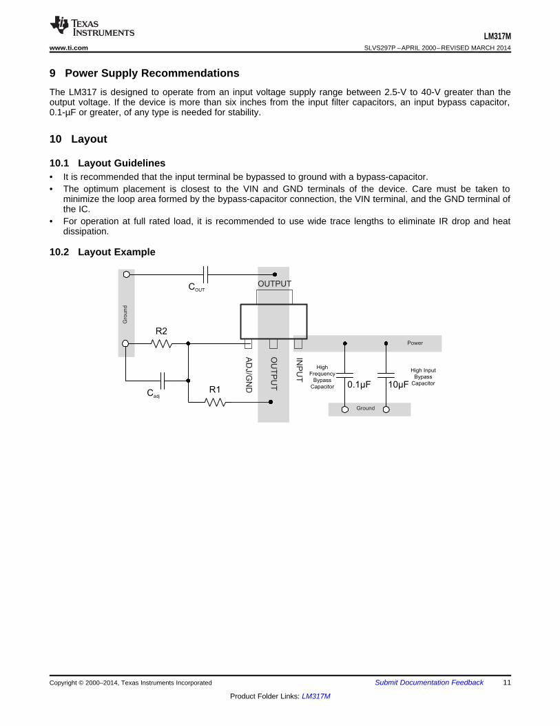
10 Layout
10.1 Layout Guidelines• It is recommended that the input terminal be bypassed to ground with a bypass-capacitor.• The optimum placement is closest to the VIN and GND terminals of the device. Care must be taken to
minimize the loop area formed by the bypass-capacitor connection, the VIN terminal, and the GND terminal ofthe IC.
• For operation at full rated load, it is recommended to use wide trace lengths to eliminate IR drop and heatdissipation.
10.2 Layout Example
Copyright © 2000–2014, Texas Instruments Incorporated Submit Documentation Feedback 11
Product Folder Links: LM317M
LM317MSLVS297P –APRIL 2000–REVISED MARCH 2014 www.ti.com
11 Device and Documentation Support
11.1 TrademarksAll trademarks are the property of their respective owners.
11.2 Electrostatic Discharge CautionThis integrated circuit can be damaged by ESD. Texas Instruments recommends that all integrated circuits be handled withappropriate precautions. Failure to observe proper handling and installation procedures can cause damage.
ESD damage can range from subtle performance degradation to complete device failure. Precision integrated circuits may be moresusceptible to damage because very small parametric changes could cause the device not to meet its published specifications.
11.3 GlossarySLYZ022 — TI Glossary.
This glossary lists and explains terms, acronyms and definitions.
12 Mechanical, Packaging, and Orderable InformationThe following pages include mechanical packaging and orderable information. This information is the mostcurrent data available for the designated devices. This data is subject to change without notice and revision ofthis document. For browser-based versions of this data sheet, refer to the left-hand navigation.
12 Submit Documentation Feedback Copyright © 2000–2014, Texas Instruments Incorporated
Product Folder Links: LM317M
PACKAGE OPTION ADDENDUM
www.ti.com 17-Mar-2017
Addendum-Page 1
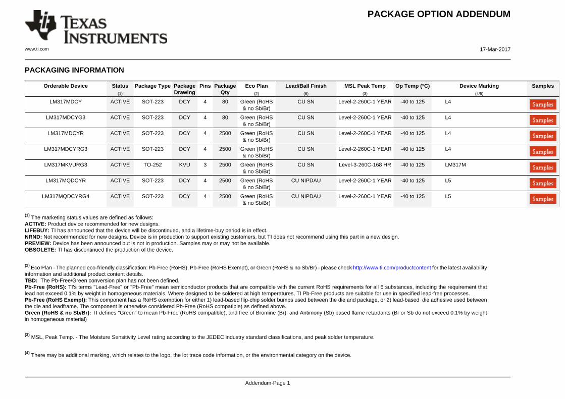
PACKAGING INFORMATION
Orderable Device Status(1)
Package Type PackageDrawing
Pins PackageQty
Eco Plan(2)
Lead/Ball Finish(6)
MSL Peak Temp(3)
Op Temp (°C) Device Marking(4/5)
Samples
LM317MDCY ACTIVE SOT-223 DCY 4 80 Green (RoHS& no Sb/Br)
CU SN Level-2-260C-1 YEAR -40 to 125 L4
LM317MDCYG3 ACTIVE SOT-223 DCY 4 80 Green (RoHS& no Sb/Br)
CU SN Level-2-260C-1 YEAR -40 to 125 L4
LM317MDCYR ACTIVE SOT-223 DCY 4 2500 Green (RoHS& no Sb/Br)
CU SN Level-2-260C-1 YEAR -40 to 125 L4
LM317MDCYRG3 ACTIVE SOT-223 DCY 4 2500 Green (RoHS& no Sb/Br)
CU SN Level-2-260C-1 YEAR -40 to 125 L4
LM317MKVURG3 ACTIVE TO-252 KVU 3 2500 Green (RoHS& no Sb/Br)
CU SN Level-3-260C-168 HR -40 to 125 LM317M
LM317MQDCYR ACTIVE SOT-223 DCY 4 2500 Green (RoHS& no Sb/Br)
CU NIPDAU Level-2-260C-1 YEAR -40 to 125 L5
LM317MQDCYRG4 ACTIVE SOT-223 DCY 4 2500 Green (RoHS& no Sb/Br)
CU NIPDAU Level-2-260C-1 YEAR -40 to 125 L5
(1) The marketing status values are defined as follows:ACTIVE: Product device recommended for new designs.LIFEBUY: TI has announced that the device will be discontinued, and a lifetime-buy period is in effect.NRND: Not recommended for new designs. Device is in production to support existing customers, but TI does not recommend using this part in a new design.PREVIEW: Device has been announced but is not in production. Samples may or may not be available.OBSOLETE: TI has discontinued the production of the device.
(2) Eco Plan - The planned eco-friendly classification: Pb-Free (RoHS), Pb-Free (RoHS Exempt), or Green (RoHS & no Sb/Br) - please check http://www.ti.com/productcontent for the latest availabilityinformation and additional product content details.TBD: The Pb-Free/Green conversion plan has not been defined.Pb-Free (RoHS): TI's terms "Lead-Free" or "Pb-Free" mean semiconductor products that are compatible with the current RoHS requirements for all 6 substances, including the requirement thatlead not exceed 0.1% by weight in homogeneous materials. Where designed to be soldered at high temperatures, TI Pb-Free products are suitable for use in specified lead-free processes.Pb-Free (RoHS Exempt): This component has a RoHS exemption for either 1) lead-based flip-chip solder bumps used between the die and package, or 2) lead-based die adhesive used betweenthe die and leadframe. The component is otherwise considered Pb-Free (RoHS compatible) as defined above.Green (RoHS & no Sb/Br): TI defines "Green" to mean Pb-Free (RoHS compatible), and free of Bromine (Br) and Antimony (Sb) based flame retardants (Br or Sb do not exceed 0.1% by weightin homogeneous material)
(3) MSL, Peak Temp. - The Moisture Sensitivity Level rating according to the JEDEC industry standard classifications, and peak solder temperature.
(4) There may be additional marking, which relates to the logo, the lot trace code information, or the environmental category on the device.
PACKAGE OPTION ADDENDUM
www.ti.com 17-Mar-2017
Addendum-Page 2
(5) Multiple Device Markings will be inside parentheses. Only one Device Marking contained in parentheses and separated by a "~" will appear on a device. If a line is indented then it is a continuationof the previous line and the two combined represent the entire Device Marking for that device.
(6) Lead/Ball Finish - Orderable Devices may have multiple material finish options. Finish options are separated by a vertical ruled line. Lead/Ball Finish values may wrap to two lines if the finishvalue exceeds the maximum column width.
Important Information and Disclaimer:The information provided on this page represents TI's knowledge and belief as of the date that it is provided. TI bases its knowledge and belief on informationprovided by third parties, and makes no representation or warranty as to the accuracy of such information. Efforts are underway to better integrate information from third parties. TI has taken andcontinues to take reasonable steps to provide representative and accurate information but may not have conducted destructive testing or chemical analysis on incoming materials and chemicals.TI and TI suppliers consider certain information to be proprietary, and thus CAS numbers and other limited information may not be available for release.
In no event shall TI's liability arising out of such information exceed the total purchase price of the TI part(s) at issue in this document sold by TI to Customer on an annual basis.
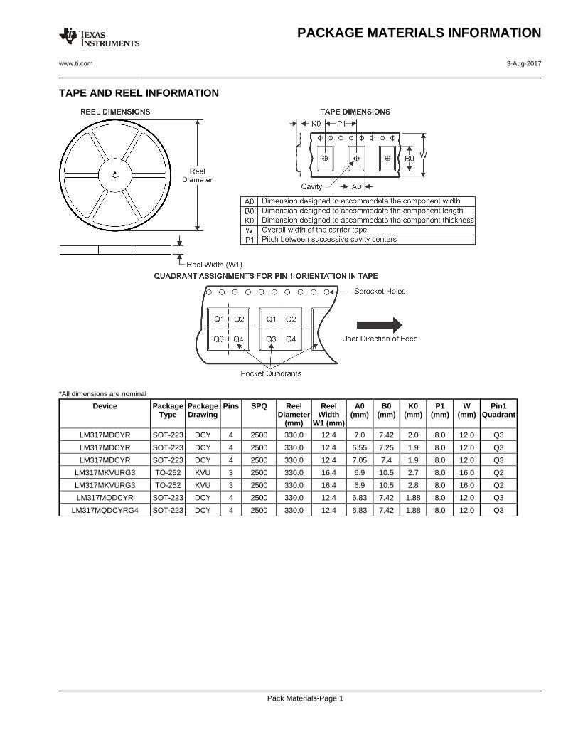
TAPE AND REEL INFORMATION
*All dimensions are nominal
Device PackageType
PackageDrawing
Pins SPQ ReelDiameter
(mm)
ReelWidth
W1 (mm)
A0(mm)
B0(mm)
K0(mm)
P1(mm)
W(mm)
Pin1Quadrant
LM317MDCYR SOT-223 DCY 4 2500 330.0 12.4 7.0 7.42 2.0 8.0 12.0 Q3
LM317MDCYR SOT-223 DCY 4 2500 330.0 12.4 6.55 7.25 1.9 8.0 12.0 Q3
LM317MDCYR SOT-223 DCY 4 2500 330.0 12.4 7.05 7.4 1.9 8.0 12.0 Q3
LM317MKVURG3 TO-252 KVU 3 2500 330.0 16.4 6.9 10.5 2.7 8.0 16.0 Q2
LM317MKVURG3 TO-252 KVU 3 2500 330.0 16.4 6.9 10.5 2.8 8.0 16.0 Q2
LM317MQDCYR SOT-223 DCY 4 2500 330.0 12.4 6.83 7.42 1.88 8.0 12.0 Q3
LM317MQDCYRG4 SOT-223 DCY 4 2500 330.0 12.4 6.83 7.42 1.88 8.0 12.0 Q3
PACKAGE MATERIALS INFORMATION
www.ti.com 3-Aug-2017
Pack Materials-Page 1
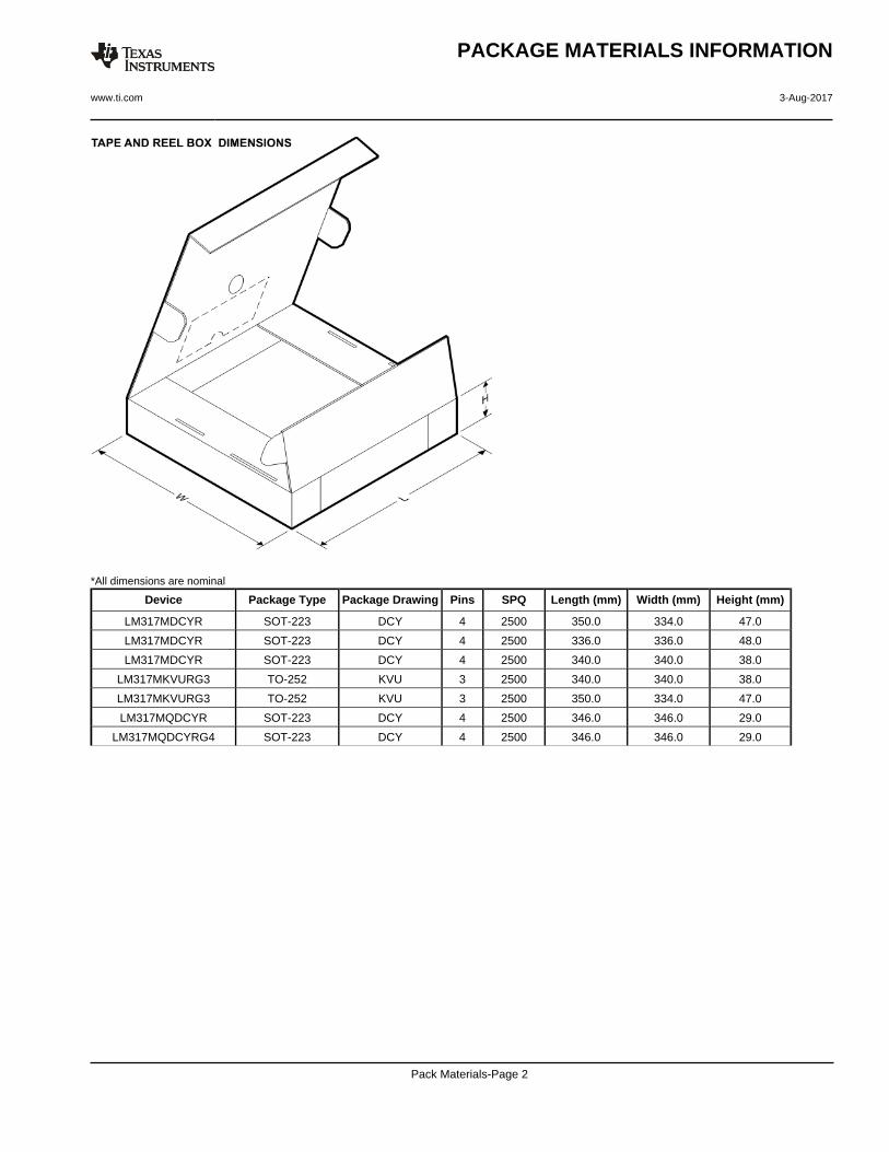
*All dimensions are nominal
Device Package Type Package Drawing Pins SPQ Length (mm) Width (mm) Height (mm)
LM317MDCYR SOT-223 DCY 4 2500 350.0 334.0 47.0
LM317MDCYR SOT-223 DCY 4 2500 336.0 336.0 48.0
LM317MDCYR SOT-223 DCY 4 2500 340.0 340.0 38.0
LM317MKVURG3 TO-252 KVU 3 2500 340.0 340.0 38.0
LM317MKVURG3 TO-252 KVU 3 2500 350.0 334.0 47.0
LM317MQDCYR SOT-223 DCY 4 2500 346.0 346.0 29.0
LM317MQDCYRG4 SOT-223 DCY 4 2500 346.0 346.0 29.0
PACKAGE MATERIALS INFORMATION
www.ti.com 3-Aug-2017
Pack Materials-Page 2
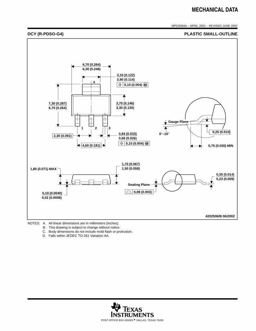
MECHANICAL DATA
MPDS094A – APRIL 2001 – REVISED JUNE 2002
POST OFFICE BOX 655303 • DALLAS, TEXAS 75265
DCY (R-PDSO-G4) PLASTIC SMALL-OUTLINE
4202506/B 06/2002
6,30 (0.248)6,70 (0.264)
2,90 (0.114)3,10 (0.122)
6,70 (0.264)7,30 (0.287) 3,70 (0.146)
3,30 (0.130)
0,02 (0.0008)0,10 (0.0040)
1,50 (0.059)1,70 (0.067)
0,23 (0.009)0,35 (0.014)
1 2 3
4
0,66 (0.026)0,84 (0.033)
1,80 (0.071) MAX
Seating Plane
0°–10°
Gauge Plane
0,75 (0.030) MIN
0,25 (0.010)
0,08 (0.003)
0,10 (0.004) M
2,30 (0.091)
4,60 (0.181) M0,10 (0.004)
NOTES: A. All linear dimensions are in millimeters (inches).B. This drawing is subject to change without notice.C. Body dimensions do not include mold flash or protrusion.D. Falls within JEDEC TO-261 Variation AA.
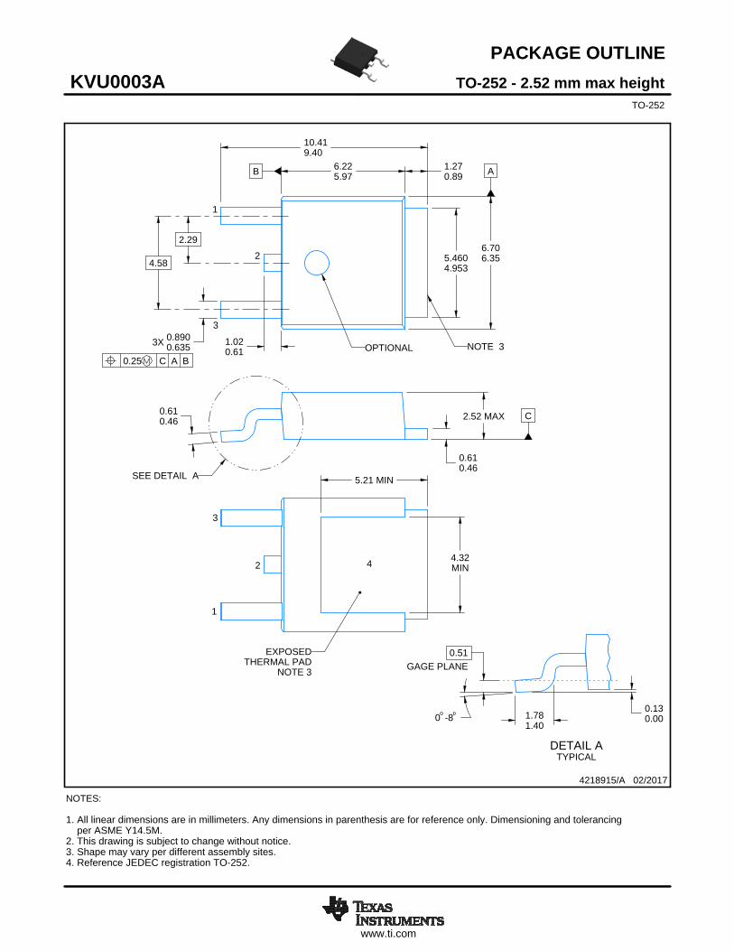
www.ti.com
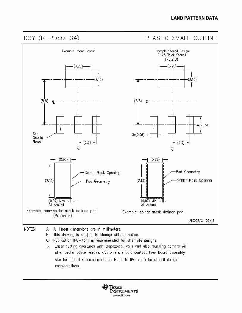
PACKAGE OUTLINE
C
5.4604.953
10.419.40
2.29
4.58
3X 0.8900.635 1.02
0.61
1.270.89
2.52 MAX
0.610.46
4.32MIN
5.21 MIN
-800.130.001.78
1.40
0.610.46
A
6.706.35
B 6.225.97
0.51GAGE PLANE
TO-252 - 2.52 mm max heightKVU0003ATO-252
4218915/A 02/2017
NOTES: 1. All linear dimensions are in millimeters. Any dimensions in parenthesis are for reference only. Dimensioning and tolerancing per ASME Y14.5M. 2. This drawing is subject to change without notice.3. Shape may vary per different assembly sites.4. Reference JEDEC registration TO-252.
1
2
3
0.25 C A BOPTIONAL NOTE 3
SCALE 1.500
SEE DETAIL A
EXPOSEDTHERMAL PAD
NOTE 3
1
2
3
4
A 7.000
DETAIL ATYPICAL
www.ti.com
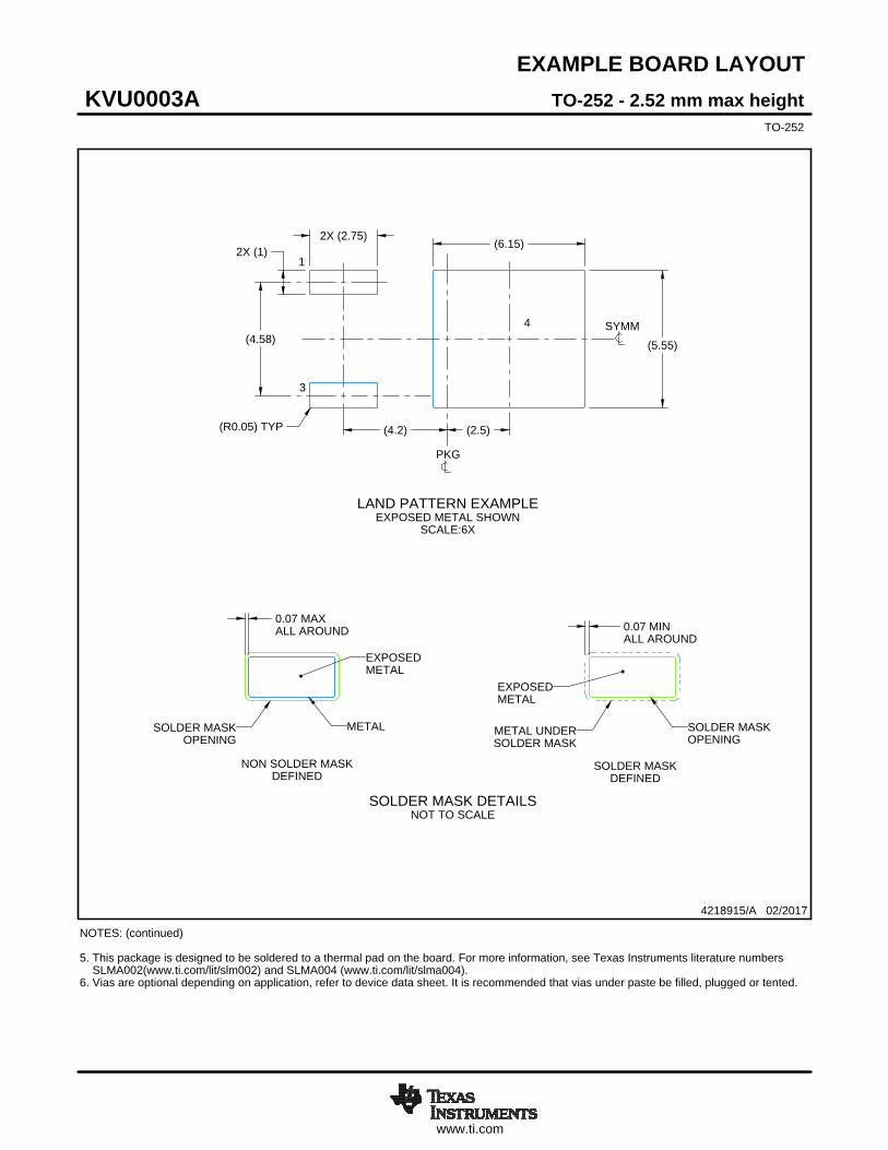
EXAMPLE BOARD LAYOUT
0.07 MAXALL AROUND 0.07 MIN
ALL AROUND
(6.15)
(5.55)(4.58)
2X (1)2X (2.75)
(4.2) (2.5)(R0.05) TYP
TO-252 - 2.52 mm max heightKVU0003ATO-252
4218915/A 02/2017
LAND PATTERN EXAMPLEEXPOSED METAL SHOWN
SCALE:6X
PKG
SYMM
3
1
4
NOTES: (continued) 5. This package is designed to be soldered to a thermal pad on the board. For more information, see Texas Instruments literature numbers SLMA002(www.ti.com/lit/slm002) and SLMA004 (www.ti.com/lit/slma004).6. Vias are optional depending on application, refer to device data sheet. It is recommended that vias under paste be filled, plugged or tented.
SOLDER MASKOPENING
METAL
EXPOSEDMETAL
SOLDER MASK DETAILSNOT TO SCALE
NON SOLDER MASKDEFINED
METAL UNDERSOLDER MASK
SOLDER MASKOPENING
EXPOSEDMETAL
SOLDER MASKDEFINED
www.ti.com
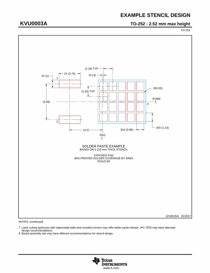
EXAMPLE STENCIL DESIGN
20X (0.98)20X (1.13)
(R0.05)
2X (2.75)2X (1)
(4.58)
(1.33) TYP
(1.18) TYP
(0.14)
(4.2)
TO-252 - 2.52 mm max heightKVU0003ATO-252
4218915/A 02/2017
PKG
NOTES: (continued) 7. Laser cutting apertures with trapezoidal walls and rounded corners may offer better paste release. IPC-7525 may have alternate design recommendations.8. Board assembly site may have different recommendations for stencil design.
SOLDER PASTE EXAMPLEBASED ON 0.125 mm THICK STENCIL
EXPOSED PAD
65% PRINTED SOLDER COVERAGE BY AREASCALE:8X
SYMM
3
1
4
IMPORTANT NOTICE
Texas Instruments Incorporated (TI) reserves the right to make corrections, enhancements, improvements and other changes to itssemiconductor products and services per JESD46, latest issue, and to discontinue any product or service per JESD48, latest issue. Buyersshould obtain the latest relevant information before placing orders and should verify that such information is current and complete.TI’s published terms of sale for semiconductor products (http://www.ti.com/sc/docs/stdterms.htm) apply to the sale of packaged integratedcircuit products that TI has qualified and released to market. Additional terms may apply to the use or sale of other types of TI products andservices.Reproduction of significant portions of TI information in TI data sheets is permissible only if reproduction is without alteration and isaccompanied by all associated warranties, conditions, limitations, and notices. TI is not responsible or liable for such reproduceddocumentation. Information of third parties may be subject to additional restrictions. Resale of TI products or services with statementsdifferent from or beyond the parameters stated by TI for that product or service voids all express and any implied warranties for theassociated TI product or service and is an unfair and deceptive business practice. TI is not responsible or liable for any such statements.Buyers and others who are developing systems that incorporate TI products (collectively, “Designers”) understand and agree that Designersremain responsible for using their independent analysis, evaluation and judgment in designing their applications and that Designers havefull and exclusive responsibility to assure the safety of Designers' applications and compliance of their applications (and of all TI productsused in or for Designers’ applications) with all applicable regulations, laws and other applicable requirements. Designer represents that, withrespect to their applications, Designer has all the necessary expertise to create and implement safeguards that (1) anticipate dangerousconsequences of failures, (2) monitor failures and their consequences, and (3) lessen the likelihood of failures that might cause harm andtake appropriate actions. Designer agrees that prior to using or distributing any applications that include TI products, Designer willthoroughly test such applications and the functionality of such TI products as used in such applications.TI’s provision of technical, application or other design advice, quality characterization, reliability data or other services or information,including, but not limited to, reference designs and materials relating to evaluation modules, (collectively, “TI Resources”) are intended toassist designers who are developing applications that incorporate TI products; by downloading, accessing or using TI Resources in anyway, Designer (individually or, if Designer is acting on behalf of a company, Designer’s company) agrees to use any particular TI Resourcesolely for this purpose and subject to the terms of this Notice.TI’s provision of TI Resources does not expand or otherwise alter TI’s applicable published warranties or warranty disclaimers for TIproducts, and no additional obligations or liabilities arise from TI providing such TI Resources. TI reserves the right to make corrections,enhancements, improvements and other changes to its TI Resources. TI has not conducted any testing other than that specificallydescribed in the published documentation for a particular TI Resource.Designer is authorized to use, copy and modify any individual TI Resource only in connection with the development of applications thatinclude the TI product(s) identified in such TI Resource. NO OTHER LICENSE, EXPRESS OR IMPLIED, BY ESTOPPEL OR OTHERWISETO ANY OTHER TI INTELLECTUAL PROPERTY RIGHT, AND NO LICENSE TO ANY TECHNOLOGY OR INTELLECTUAL PROPERTYRIGHT OF TI OR ANY THIRD PARTY IS GRANTED HEREIN, including but not limited to any patent right, copyright, mask work right, orother intellectual property right relating to any combination, machine, or process in which TI products or services are used. Informationregarding or referencing third-party products or services does not constitute a license to use such products or services, or a warranty orendorsement thereof. Use of TI Resources may require a license from a third party under the patents or other intellectual property of thethird party, or a license from TI under the patents or other intellectual property of TI.TI RESOURCES ARE PROVIDED “AS IS” AND WITH ALL FAULTS. TI DISCLAIMS ALL OTHER WARRANTIES ORREPRESENTATIONS, EXPRESS OR IMPLIED, REGARDING RESOURCES OR USE THEREOF, INCLUDING BUT NOT LIMITED TOACCURACY OR COMPLETENESS, TITLE, ANY EPIDEMIC FAILURE WARRANTY AND ANY IMPLIED WARRANTIES OFMERCHANTABILITY, FITNESS FOR A PARTICULAR PURPOSE, AND NON-INFRINGEMENT OF ANY THIRD PARTY INTELLECTUALPROPERTY RIGHTS. TI SHALL NOT BE LIABLE FOR AND SHALL NOT DEFEND OR INDEMNIFY DESIGNER AGAINST ANY CLAIM,INCLUDING BUT NOT LIMITED TO ANY INFRINGEMENT CLAIM THAT RELATES TO OR IS BASED ON ANY COMBINATION OFPRODUCTS EVEN IF DESCRIBED IN TI RESOURCES OR OTHERWISE. IN NO EVENT SHALL TI BE LIABLE FOR ANY ACTUAL,DIRECT, SPECIAL, COLLATERAL, INDIRECT, PUNITIVE, INCIDENTAL, CONSEQUENTIAL OR EXEMPLARY DAMAGES INCONNECTION WITH OR ARISING OUT OF TI RESOURCES OR USE THEREOF, AND REGARDLESS OF WHETHER TI HAS BEENADVISED OF THE POSSIBILITY OF SUCH DAMAGES.Unless TI has explicitly designated an individual product as meeting the requirements of a particular industry standard (e.g., ISO/TS 16949and ISO 26262), TI is not responsible for any failure to meet such industry standard requirements.Where TI specifically promotes products as facilitating functional safety or as compliant with industry functional safety standards, suchproducts are intended to help enable customers to design and create their own applications that meet applicable functional safety standardsand requirements. Using products in an application does not by itself establish any safety features in the application. Designers mustensure compliance with safety-related requirements and standards applicable to their applications. Designer may not use any TI products inlife-critical medical equipment unless authorized officers of the parties have executed a special contract specifically governing such use.Life-critical medical equipment is medical equipment where failure of such equipment would cause serious bodily injury or death (e.g., lifesupport, pacemakers, defibrillators, heart pumps, neurostimulators, and implantables). Such equipment includes, without limitation, allmedical devices identified by the U.S. Food and Drug Administration as Class III devices and equivalent classifications outside the U.S.TI may expressly designate certain products as completing a particular qualification (e.g., Q100, Military Grade, or Enhanced Product).Designers agree that it has the necessary expertise to select the product with the appropriate qualification designation for their applicationsand that proper product selection is at Designers’ own risk. Designers are solely responsible for compliance with all legal and regulatoryrequirements in connection with such selection.Designer will fully indemnify TI and its representatives against any damages, costs, losses, and/or liabilities arising out of Designer’s non-compliance with the terms and provisions of this Notice.
Mailing Address: Texas Instruments, Post Office Box 655303, Dallas, Texas 75265Copyright © 2017, Texas Instruments Incorporated