RF and Microwave Challenges for Future Radio Spectrum...
33
1 RF and Microwave Challenges for Future Radio Spectrum Access Larry Larson Dean – School of Engineering [email protected]
Transcript of RF and Microwave Challenges for Future Radio Spectrum...
1
RF and Microwave Challenges for Future
Radio Spectrum Access
Larry Larson
Dean – School of Engineering [email protected]
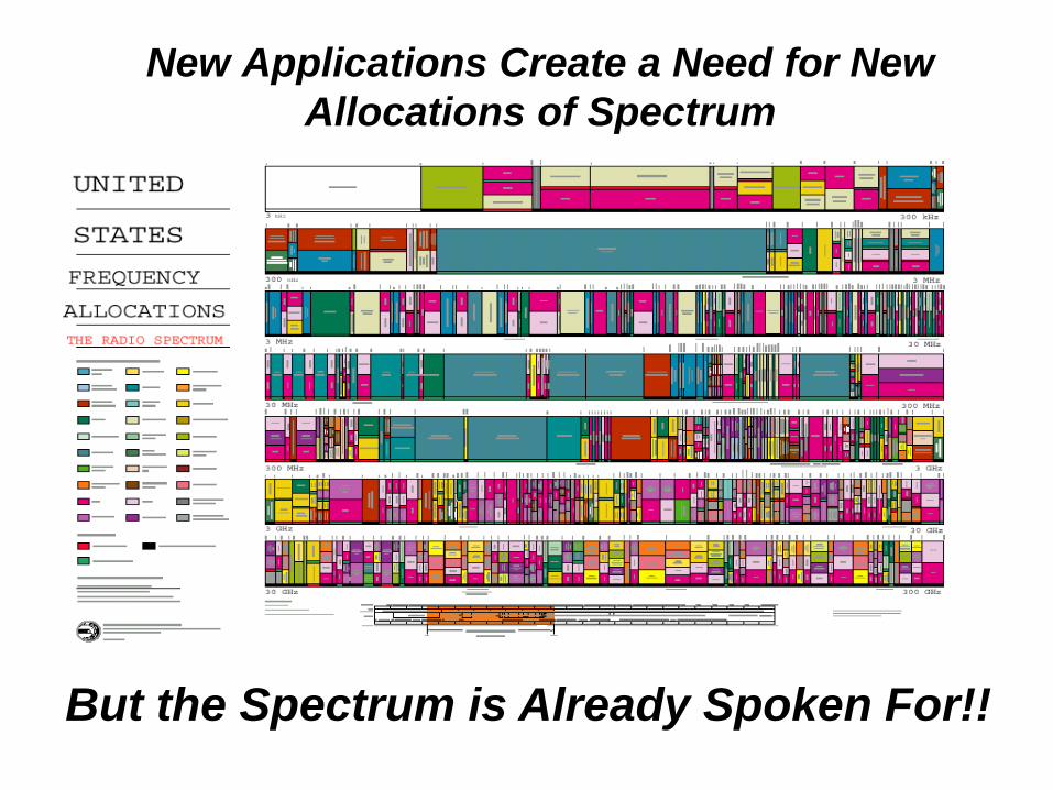
New Applications Create a Need for New
Allocations of Spectrum
But the Spectrum is Already Spoken For!!
3
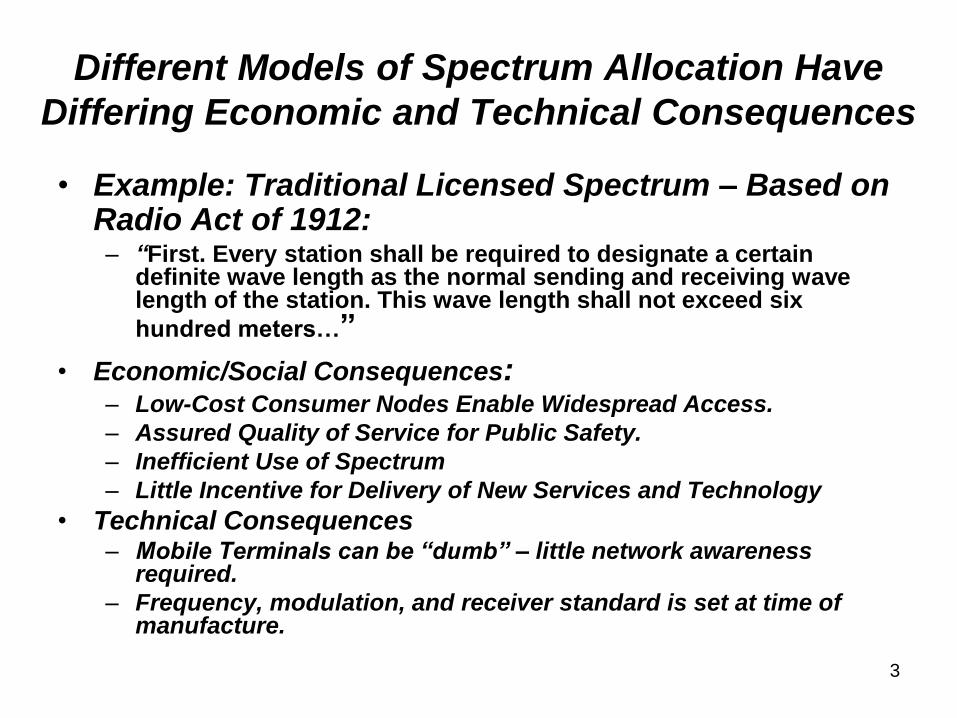
Different Models of Spectrum Allocation Have
Differing Economic and Technical Consequences
• Example: Traditional Licensed Spectrum – Based on Radio Act of 1912: – “First. Every station shall be required to designate a certain
definite wave length as the normal sending and receiving wave length of the station. This wave length shall not exceed six
hundred meters…”
• Economic/Social Consequences: – Low-Cost Consumer Nodes Enable Widespread Access.
– Assured Quality of Service for Public Safety.
– Inefficient Use of Spectrum
– Little Incentive for Delivery of New Services and Technology
• Technical Consequences – Mobile Terminals can be “dumb” – little network awareness
required.
– Frequency, modulation, and receiver standard is set at time of manufacture.
4
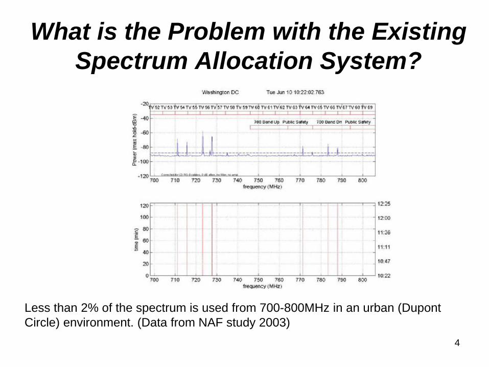
What is the Problem with the Existing
Spectrum Allocation System?
Less than 2% of the spectrum is used from 700-800MHz in an urban (Dupont
Circle) environment. (Data from NAF study 2003)
5
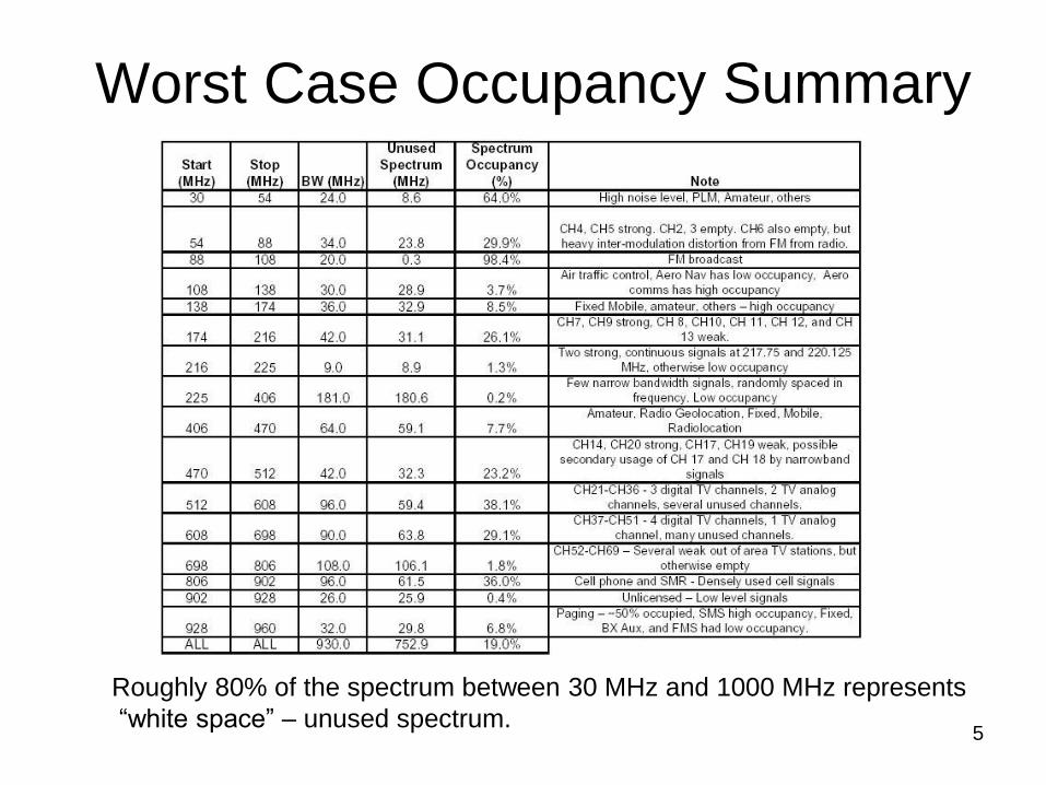
Worst Case Occupancy Summary
Roughly 80% of the spectrum between 30 MHz and 1000 MHz represents
“white space” – unused spectrum.

Spectrum Use in Practice
(Wan Vazer) • Some spectrum is
intensively used
• Other spectrum has
highly variable use in
when viewed in terms of
time and geography
7
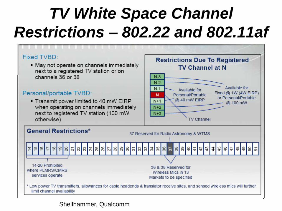
TV White Space Channel
Restrictions – 802.22 and 802.11af
Shellhammer, Qualcomm
8
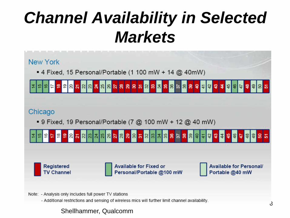
Channel Availability in Selected
Markets
Shellhammer, Qualcomm
9
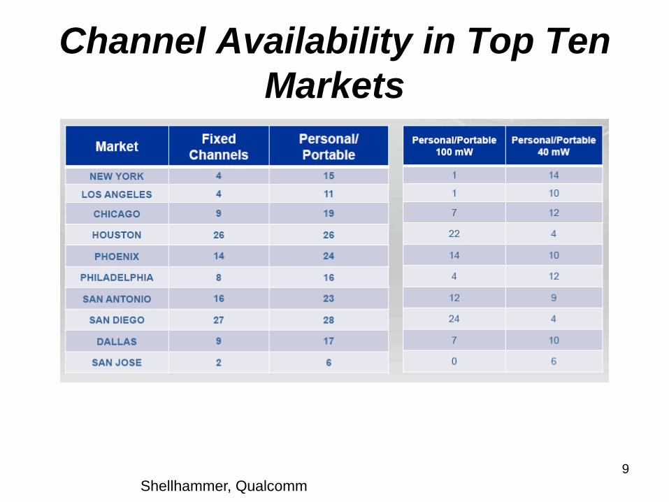
Channel Availability in Top Ten
Markets
Shellhammer, Qualcomm
10
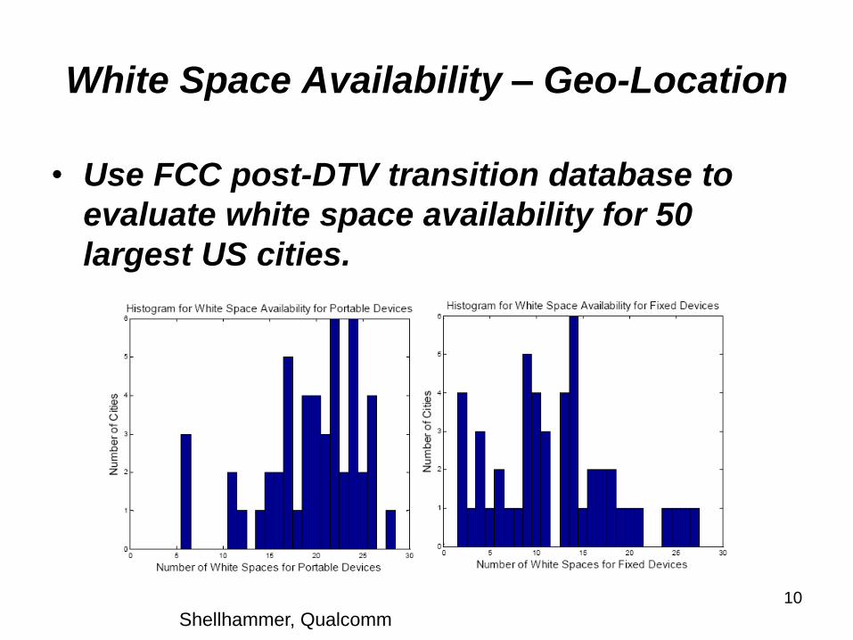
White Space Availability – Geo-Location
• Use FCC post-DTV transition database to
evaluate white space availability for 50
largest US cities.
Shellhammer, Qualcomm
11
Geo-location Challenges
• Geo-location database access:
– Required for Fixed and Portable Services to +/- 50 meters
– Fixed Devices: Geo-Location known at installation
– Portable Devices: Geo-location must use GPS, but…
• Indoor GPS is not always reliable
• Physical layer ranging my be inaccurate due to shadowing and multi-path effect.
12
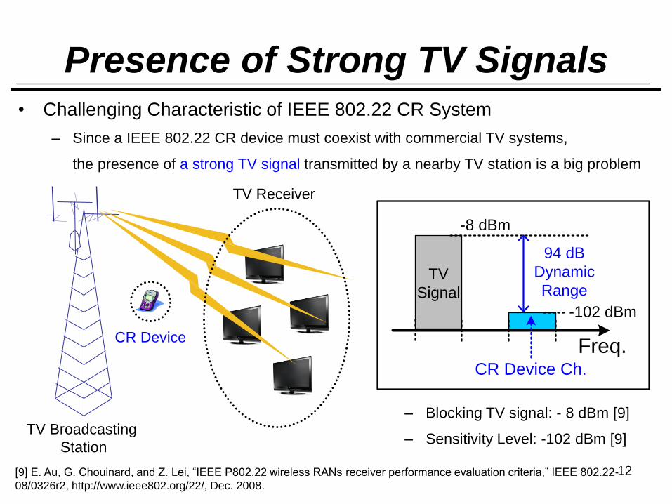
• Challenging Characteristic of IEEE 802.22 CR System
– Since a IEEE 802.22 CR device must coexist with commercial TV systems,
the presence of a strong TV signal transmitted by a nearby TV station is a big problem
[9] E. Au, G. Chouinard, and Z. Lei, “IEEE P802.22 wireless RANs receiver performance evaluation criteria,” IEEE 802.22-
08/0326r2, http://www.ieee802.org/22/, Dec. 2008.
– Blocking TV signal: - 8 dBm [9]
– Sensitivity Level: -102 dBm [9] TV Broadcasting
Station
CR Device
TV Receiver
Freq.CR Device Ch.
TV
Signal
-8 dBm
-102 dBm
94 dB
Dynamic
Range
Presence of Strong TV Signals
13
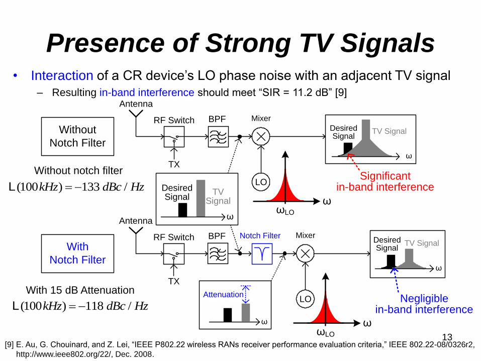
Presence of Strong TV Signals • Interaction of a CR device’s LO phase noise with an adjacent TV signal
– Resulting in-band interference should meet “SIR = 11.2 dB” [9]
[9] E. Au, G. Chouinard, and Z. Lei, “IEEE P802.22 wireless RANs receiver performance evaluation criteria,” IEEE 802.22-08/0326r2,
http://www.ieee802.org/22/, Dec. 2008.
(100 ) 133 /kHz dBc Hz L
Without notch filter
With 15 dB Attenuation
(100 ) 118 /kHz dBc Hz L
Notch Filter
Antenna
RF Switch
TX
Mixer
LO
Without
Notch Filter
BPF
ωLO
ω
Antenna
RF Switch
TX
Mixer
LO
BPF
ωLO
ω
With
Notch Filter
TVSignal
DesiredSignal
ω
TV Signal
ω
DesiredSignal
Significant in-band interference
TV Signal
ω
DesiredSignal
Negligiblein-band interference
Attenuation
ω
14
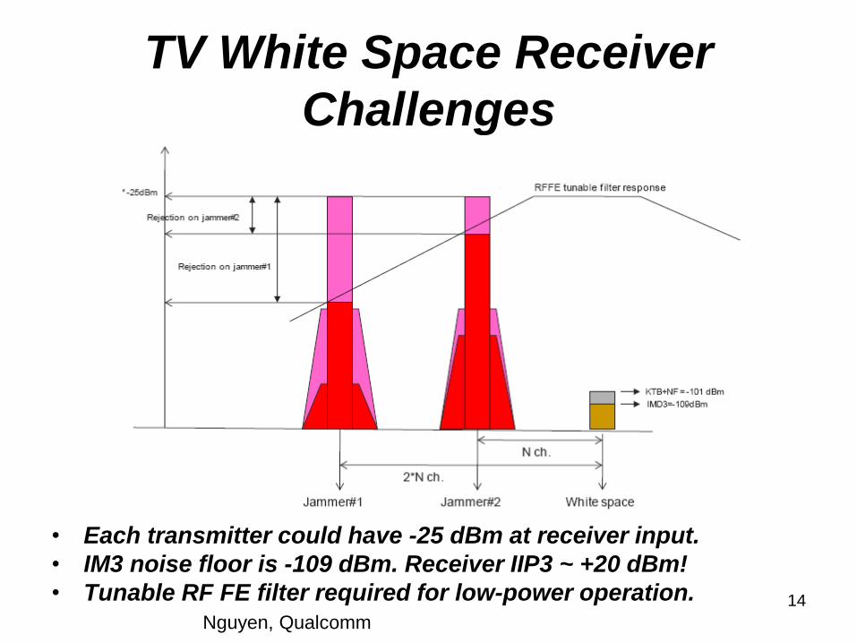
TV White Space Receiver
Challenges
• Each transmitter could have -25 dBm at receiver input.
• IM3 noise floor is -109 dBm. Receiver IIP3 ~ +20 dBm!
• Tunable RF FE filter required for low-power operation.
Nguyen, Qualcomm
15
TV White Space Receiver
Challenges
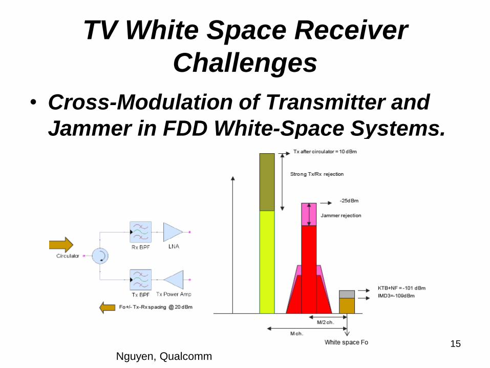
• Cross-Modulation of Transmitter and
Jammer in FDD White-Space Systems.
Nguyen, Qualcomm
16
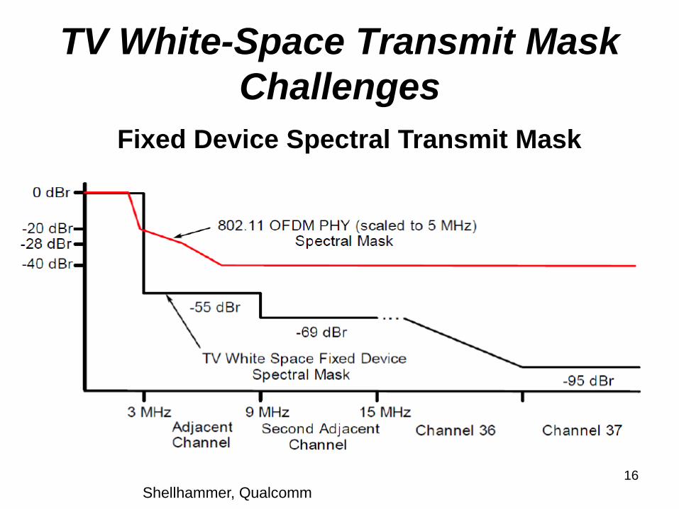
TV White-Space Transmit Mask
Challenges
Fixed Device Spectral Transmit Mask
Shellhammer, Qualcomm
17
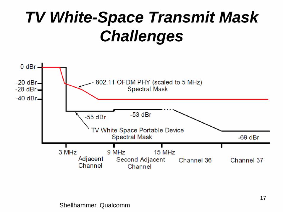
TV White-Space Transmit Mask
Challenges
Shellhammer, Qualcomm
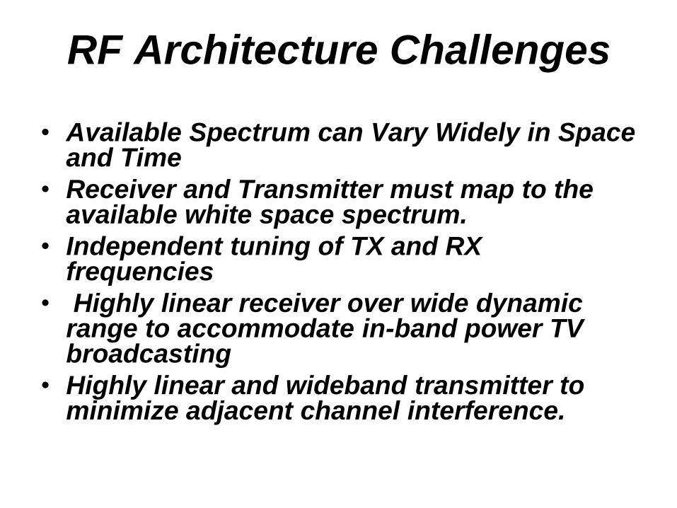
RF Architecture Challenges
• Available Spectrum can Vary Widely in Space and Time
• Receiver and Transmitter must map to the available white space spectrum.
• Independent tuning of TX and RX frequencies
• Highly linear receiver over wide dynamic range to accommodate in-band power TV broadcasting
• Highly linear and wideband transmitter to minimize adjacent channel interference.
19
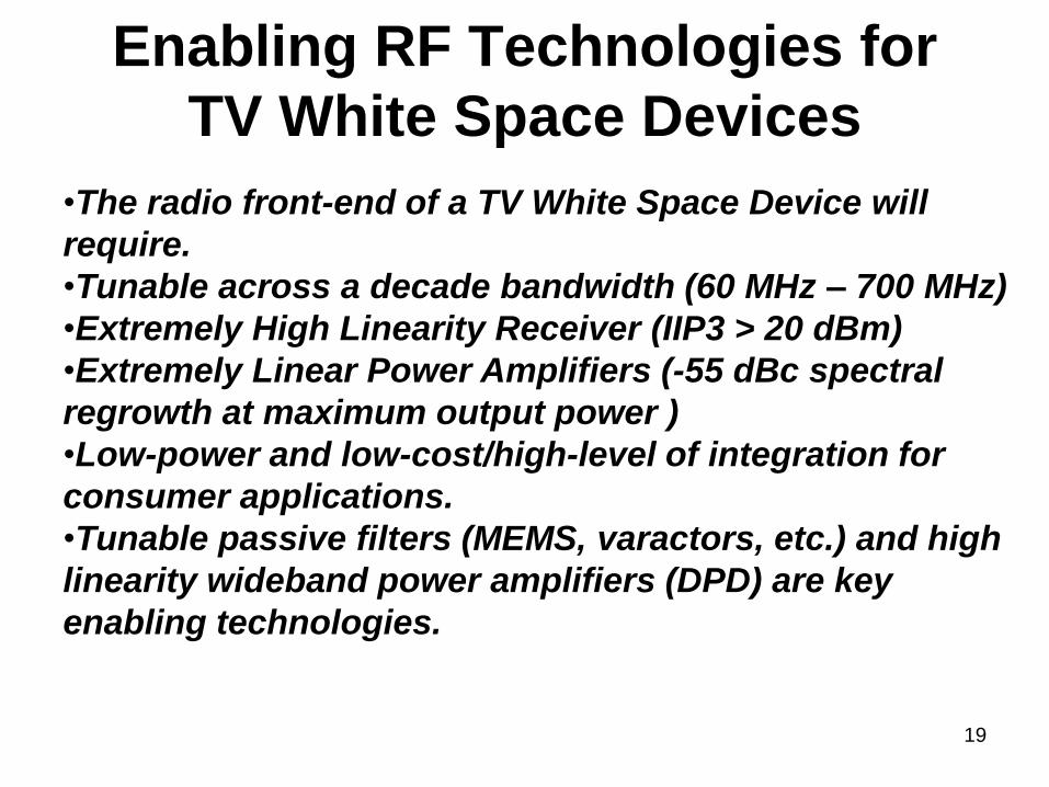
Enabling RF Technologies for
TV White Space Devices
•The radio front-end of a TV White Space Device will
require.
•Tunable across a decade bandwidth (60 MHz – 700 MHz)
•Extremely High Linearity Receiver (IIP3 > 20 dBm)
•Extremely Linear Power Amplifiers (-55 dBc spectral
regrowth at maximum output power )
•Low-power and low-cost/high-level of integration for
consumer applications.
•Tunable passive filters (MEMS, varactors, etc.) and high
linearity wideband power amplifiers (DPD) are key
enabling technologies.
20
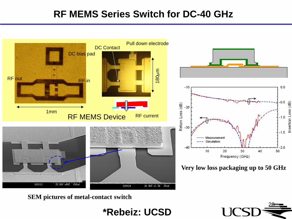
RF MEMS Series Switch for DC-40 GHz
18
0m
m
DC Contact
RF current
Pull down electrode
DC bias pad
RF in RF out
RF MEMS Device 1mm
Very low loss packaging up to 50 GHz
SEM pictures of metal-contact switch
*Rebeiz: UCSD
21
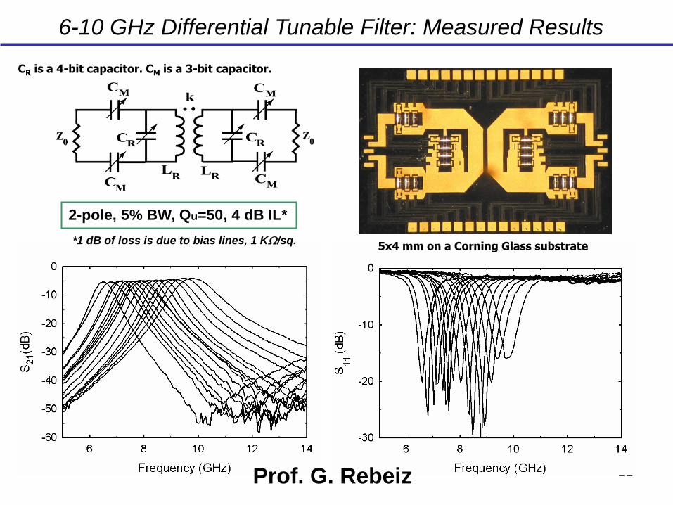
6-10 GHz Differential Tunable Filter: Measured Results
2-pole, 5% BW, Qu=50, 4 dB IL*
CR is a 4-bit capacitor. CM is a 3-bit capacitor.
*1 dB of loss is due to bias lines, 1 KW/sq. 5x4 mm on a Corning Glass substrate
Prof. G. Rebeiz
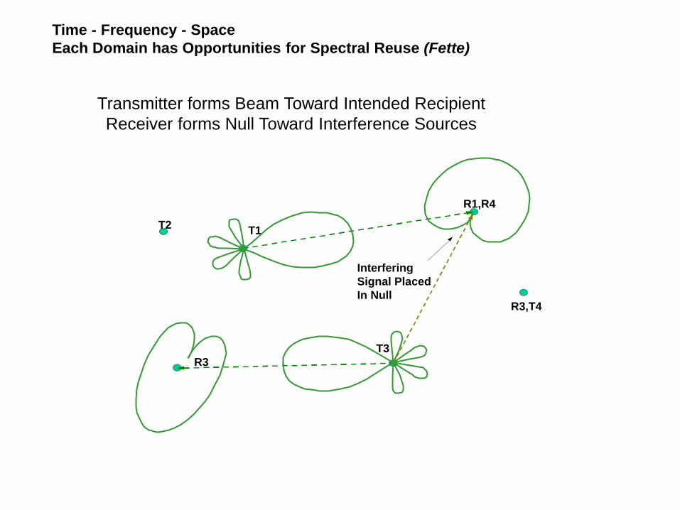
Time - Frequency - Space
Each Domain has Opportunities for Spectral Reuse (Fette)
T1
R1,R4
T2
T3
R3
R3,T4
Interfering
Signal Placed
In Null
Transmitter forms Beam Toward Intended Recipient
Receiver forms Null Toward Interference Sources
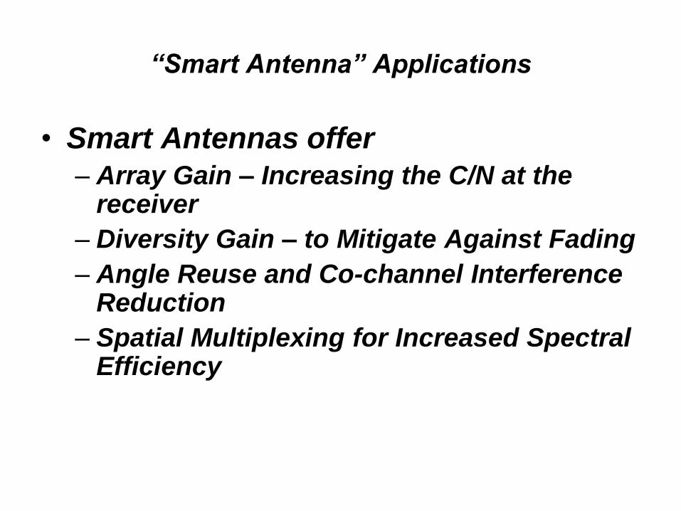
“Smart Antenna” Applications
• Smart Antennas offer
– Array Gain – Increasing the C/N at the receiver
– Diversity Gain – to Mitigate Against Fading
– Angle Reuse and Co-channel Interference Reduction
– Spatial Multiplexing for Increased Spectral Efficiency
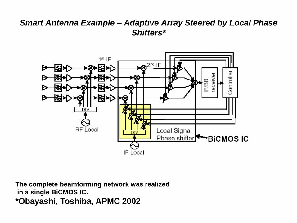
Smart Antenna Example – Adaptive Array Steered by Local Phase
Shifters*
The complete beamforming network was realized
in a single BiCMOS IC.
*Obayashi, Toshiba, APMC 2002
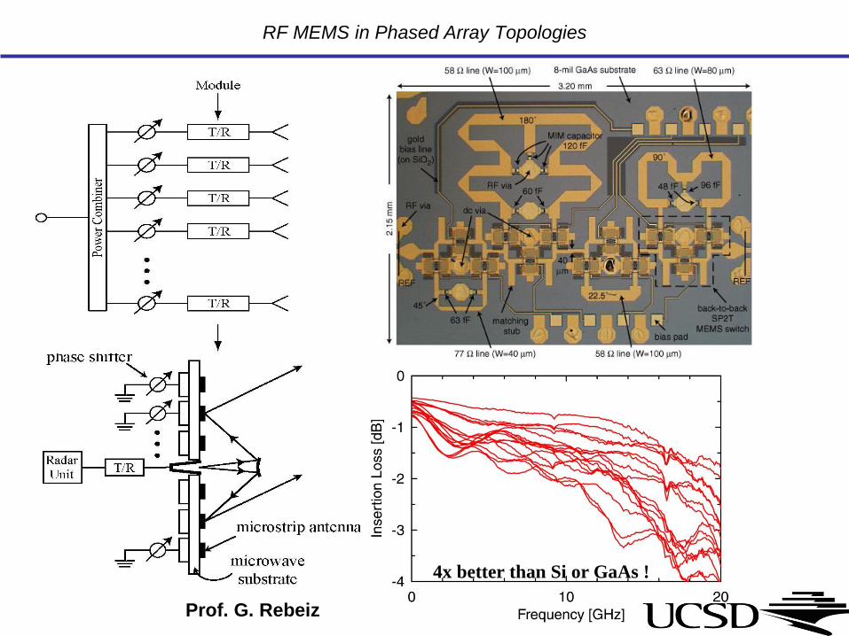
RF MEMS in Phased Array Topologies
4x better than Si or GaAs !
Prof. G. Rebeiz
26
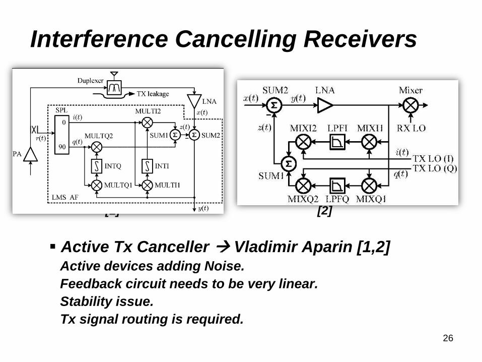
Interference Cancelling Receivers
[1] [2]
Active Tx Canceller Vladimir Aparin [1,2] Active devices adding Noise.
Feedback circuit needs to be very linear.
Stability issue.
Tx signal routing is required.
27
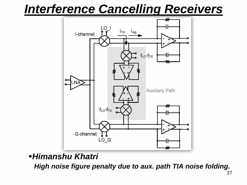
Interference Cancelling Receivers
Himanshu Khatri High noise figure penalty due to aux. path TIA noise folding.
28
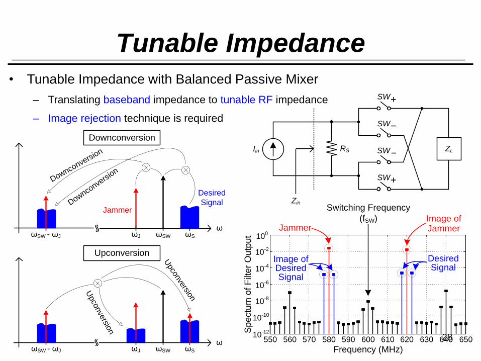
• Tunable Impedance with Balanced Passive Mixer
– Translating baseband impedance to tunable RF impedance
– Image rejection technique is required
Tunable Impedance
Iin
Zin
ZL
SW
SW
SW
SW
+
+
RS
Frequency (MHz)550 560 570 580 590 600 610 620 630 640 650
10-8
10-6
10-4
10-2
100
Sp
ectu
m o
f F
ilte
r O
utp
ut
10-10
10-12
JammerImage of Jammer
Image of Desired Signal
Desired Signal
Switching Frequency
(fSW)
Downconversion
Upconversion
Upconversion
Upco
nve
rsion
ωωSωSWωJωSW - ωJ
ωωSωSWωJωSW - ωJ
Downconve
rsion
Downconversion
Desired
SignalJammer
29
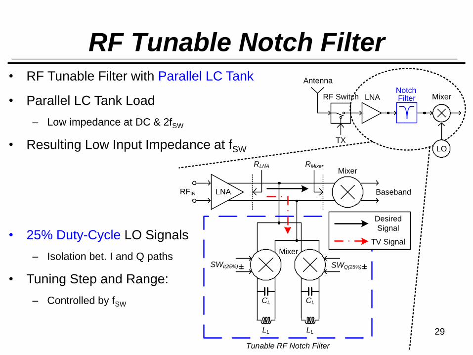
RF Tunable Notch Filter • RF Tunable Filter with Parallel LC Tank
• Parallel LC Tank Load
– Low impedance at DC & 2fSW
• Resulting Low Input Impedance at fSW
• 25% Duty-Cycle LO Signals
– Isolation bet. I and Q paths
• Tuning Step and Range:
– Controlled by fSW
LNARFIN
RLNA RMixerMixer
Baseband
SWI(25%)+
Mixer
SWQ(25%)+
Tunable RF Notch Filter
CL
LL
CL
LL
TV Signal
Desired
Signal
Antenna
RF Switch
TX
LNANotch Filter Mixer
LO
30
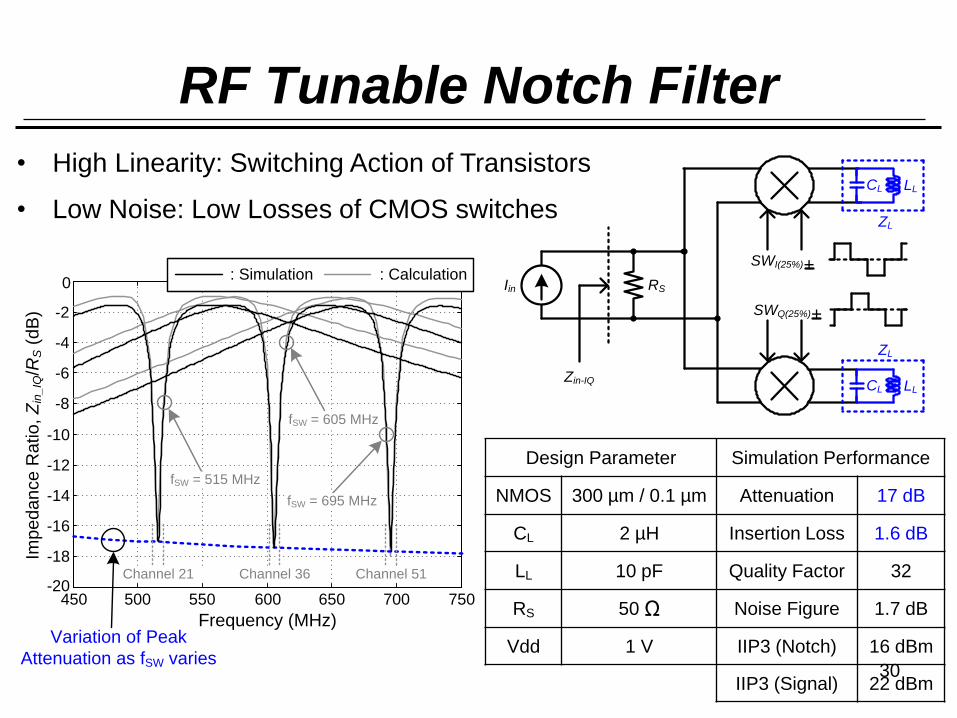
• High Linearity: Switching Action of Transistors
• Low Noise: Low Losses of CMOS switches
Design Parameter Simulation Performance
NMOS 300 µm / 0.1 µm Attenuation 17 dB
CL 2 µH Insertion Loss 1.6 dB
LL 10 pF Quality Factor 32
RS 50 Ω Noise Figure 1.7 dB
Vdd 1 V IIP3 (Notch) 16 dBm
IIP3 (Signal) 22 dBm
450 500 550 600 650 700 750-20
-18
-16
-14
-12
-10
-8
-6
-4
-2
0
Frequency (MHz)
Imp
ed
an
ce
Ra
tio
, Z
in_IQ
/RS (
dB
)
fSW = 605 MHz
fSW = 695 MHz
fSW = 515 MHz
Channel 51Channel 36Channel 21
: Simulation : Calculation
Variation of Peak
Attenuation as fSW varies
Zin-IQ
SWI(25%)+
SWQ(25%)+
Iin RS
CL LL
ZL
CL LL
ZL
RF Tunable Notch Filter
31
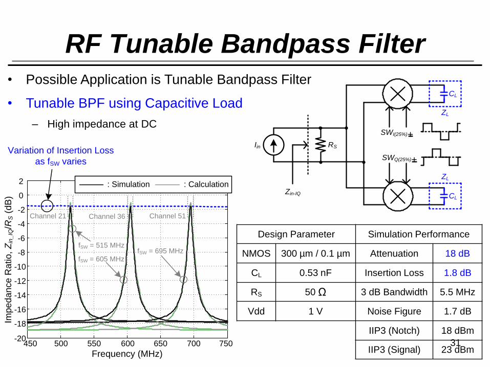
• Possible Application is Tunable Bandpass Filter
• Tunable BPF using Capacitive Load
– High impedance at DC
RF Tunable Bandpass Filter
Design Parameter Simulation Performance
NMOS 300 µm / 0.1 µm Attenuation 18 dB
CL 0.53 nF Insertion Loss 1.8 dB
RS 50 Ω 3 dB Bandwidth 5.5 MHz
Vdd 1 V Noise Figure 1.7 dB
IIP3 (Notch) 18 dBm
IIP3 (Signal) 23 dBm
Zin-IQ
SWI(25%)+
SWQ(25%)+
Iin RS
CL
ZL
CL
ZL
: Simulation : Calculation
Imp
ed
an
ce
Ra
tio
, Z
in_IQ
/RS (
dB
)
-20
-18
-16
-14
-12
-10
-8
-6
-4
-2
0
2
450 500 550 600 650 700 750
Frequency (MHz)
Channel 21 Channel 36 Channel 51
fSW = 515 MHz
fSW = 605 MHzfSW = 695 MHz
Variation of Insertion Loss
as fSW varies
32
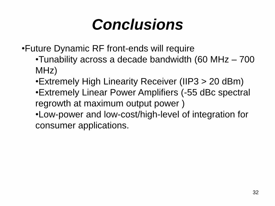
Conclusions
•Future Dynamic RF front-ends will require
•Tunability across a decade bandwidth (60 MHz – 700
MHz)
•Extremely High Linearity Receiver (IIP3 > 20 dBm)
•Extremely Linear Power Amplifiers (-55 dBc spectral
regrowth at maximum output power )
•Low-power and low-cost/high-level of integration for
consumer applications.

Thank You!
33