Left-Handed Metamaterials for Microwave Engineering ...
62
Left-Handed Metamaterials for Microwave Engineering Applications Author: Anthony Lai Advisor: Prof. Tatsuo Itoh Department of Electrical Engineering UCLA
Transcript of Left-Handed Metamaterials for Microwave Engineering ...

Left-Handed Metamaterials for Microwave Engineering ApplicationsAuthor: Anthony LaiAdvisor: Prof. Tatsuo ItohDepartment of Electrical Engineering
UCLA

Outline• Left-Handed Metamaterial Introduction
Resonant approachTransmission line approach
• Composite Right/Left-Handed Metamaterial• Metamaterial-Based Microwave Devices
Dominant leaky-wave antennaSmall, resonant backward wave antennasDual-band hybrid couplerNegative refractive index flat lens
• Future Trends• Summary
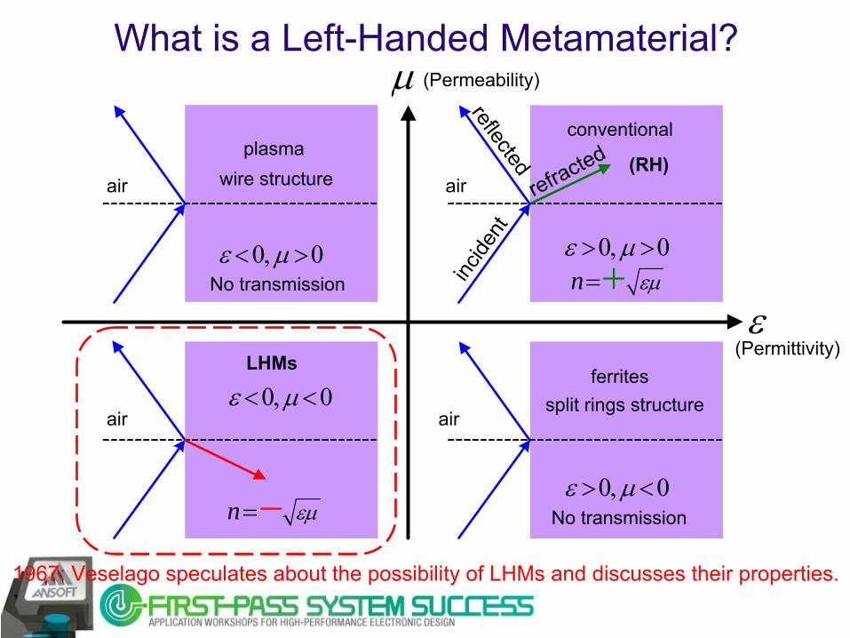
What is a Left-Handed Metamaterial?
conventionalplasma
wire structure
split rings structureferrites
LHMs
0, 0n εμε μ> >=+
0, 0ε μ> <
0, 0ε μ< <
0, 0ε μ< >
ε
μ
No transmission
No transmissionn εμ=−
(RH)air air
air air
(Permittivity)
(Permeability)
1967: Veselago speculates about the possibility of LHMs and discusses their properties.
incide
nt
refracted
reflected
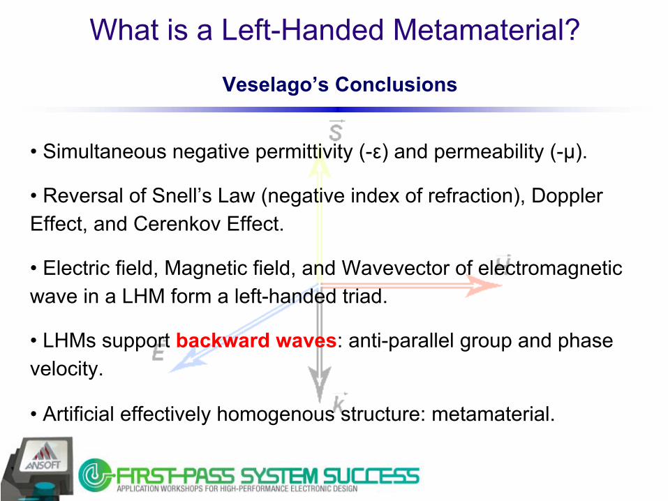
• Simultaneous negative permittivity (-ε) and permeability (-μ).
•
Reversal of Snell’s Law (negative index of refraction), Doppler Effect, and Cerenkov Effect.
•
Electric field, Magnetic field, and Wavevector of electromagnetic wave in a LHM form a left-handed triad.
•
LHMs support backward waves: anti-parallel group and phase velocity.
• Artificial effectively homogenous structure: metamaterial.
Veselago’s Conclusions
What is a Left-Handed Metamaterial?
→
k
→
k
→
k
→
S
→
S
→
S
Pin
Pout
LH Triad
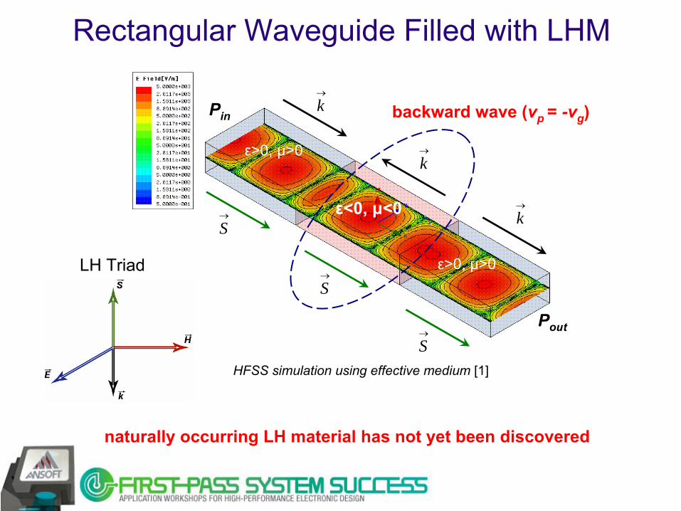
backward wave (vp
= -vg
)
Rectangular Waveguide Filled with LHM
ε<0, μ<0
ε>0, μ>0
ε>0, μ>0
HFSS simulation using effective medium [1]
naturally occurring LH material has not yet been discovered
LHM –
Resonant Approach
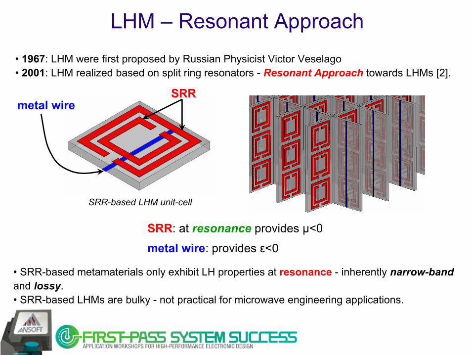
SRR-based LHM unit-cell
SRRmetal wire
• 1967: LHM were first proposed by Russian Physicist Victor Veselago • 2001: LHM realized based on split ring resonators -
Resonant Approach
towards LHMs [2].
SRR: at resonance
provides μ<0
metal wire: provides ε<0
•
SRR-based metamaterials only exhibit LH properties at resonance
-
inherently narrow-band
and lossy. • SRR-based LHMs are bulky -
not practical for microwave engineering applications.
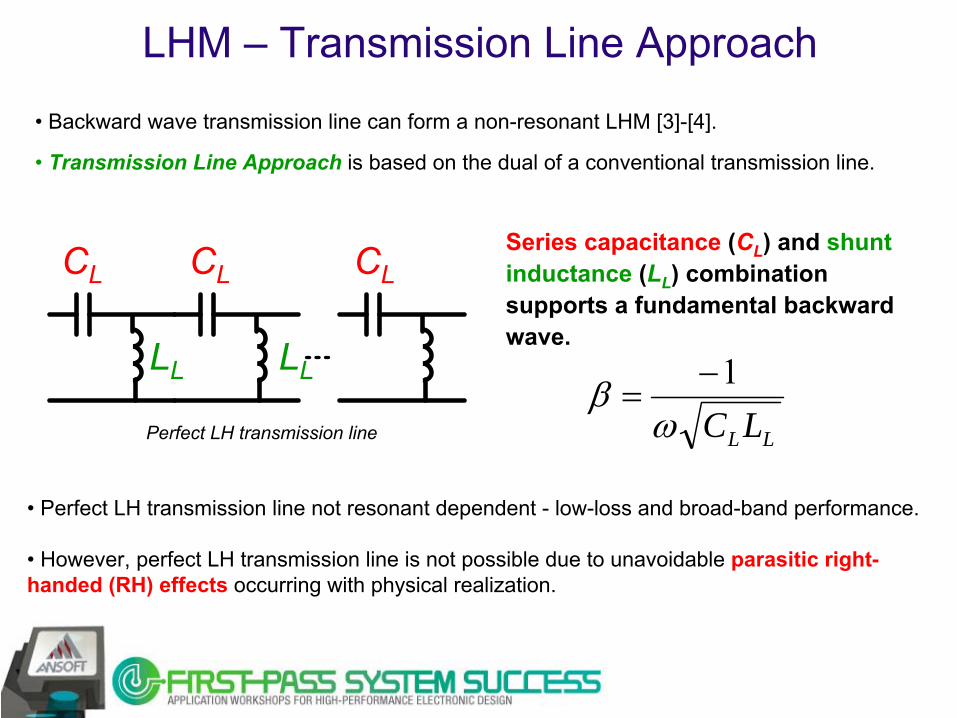
Perfect LH transmission line
LL
CL
LL
CL CL
• Backward wave transmission line can form a non-resonant LHM [3]-[4].
• Transmission Line Approach
is based on the dual of a conventional transmission line.
LHM –
Transmission Line Approach
Series capacitance
(CL
) and shunt inductance
(LL
) combination supports a fundamental backward wave.
LLLCωβ 1−=
• Perfect LH transmission line not resonant dependent -
low-loss and broad-band performance.
•
However, perfect LH transmission line is not possible due to unavoidable parasitic right-
handed (RH) effects
occurring with physical realization.
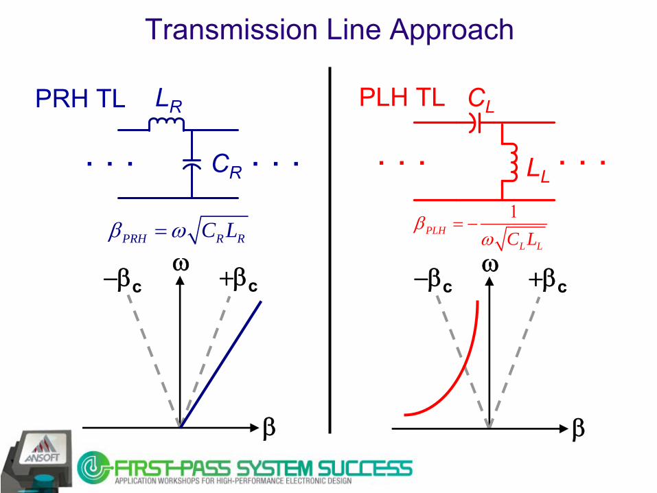
PRH R RC Lβ ω=
LR
CR LL
CL
1PLH
L LC Lβ
ω= −
PRH TL PLH TL
ω +βc−βc
β
+βc−βc
β
ω
. . . . . . . . . . . .
Transmission Line Approach
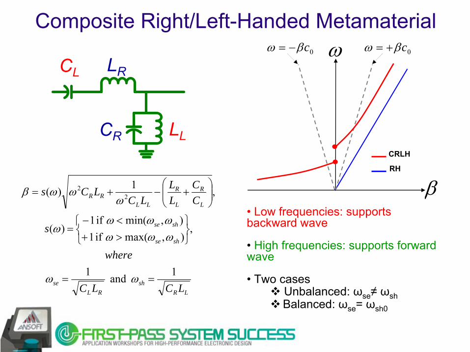
β
ω0cβω −= 0cβω +=
CRLH
RH
LR
CR
CL
LL
•
Low frequencies: supports backward wave
•
High frequencies: supports forward wave
• Two casesUnbalanced: ωse≠ ωshBalanced: ωse= ωsh0
Composite Right/Left-Handed Metamaterial
LRsh
RLse
shse
shse
L
R
L
R
LLRR
LCLC
where
s
CC
LL
LCLCs
1 and 1
,),max( if 1),min( if 1
)(
,1)( 22
==
⎭⎬⎫
⎩⎨⎧
>+<−
=
⎟⎟⎠
⎞⎜⎜⎝
⎛+−+=
ωω
ωωωωωω
ω
ωωωβ
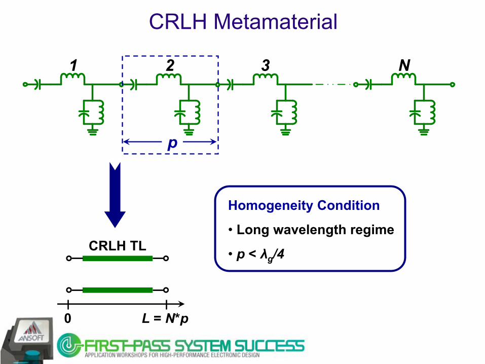
CRLH Metamaterial
CRLH TL
0 L = N*p
1 2 3 N
p
Homogeneity Condition
• Long wavelength regime
• p < λg
/4
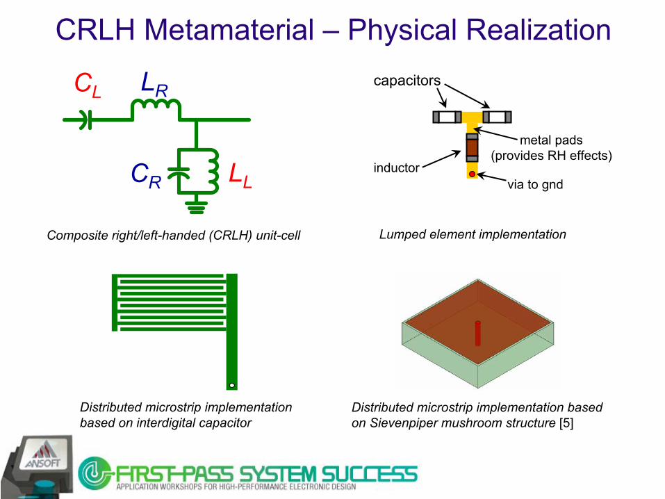
CRLH Metamaterial –
Physical Realization
LR
CR
CL
LL
Composite right/left-handed (CRLH) unit-cell Lumped element implementation
capacitors
inductorvia to gnd
metal pads
(provides RH effects)
Distributed microstrip implementation based on interdigital capacitor
Distributed microstrip implementation based on Sievenpiper mushroom structure [5]
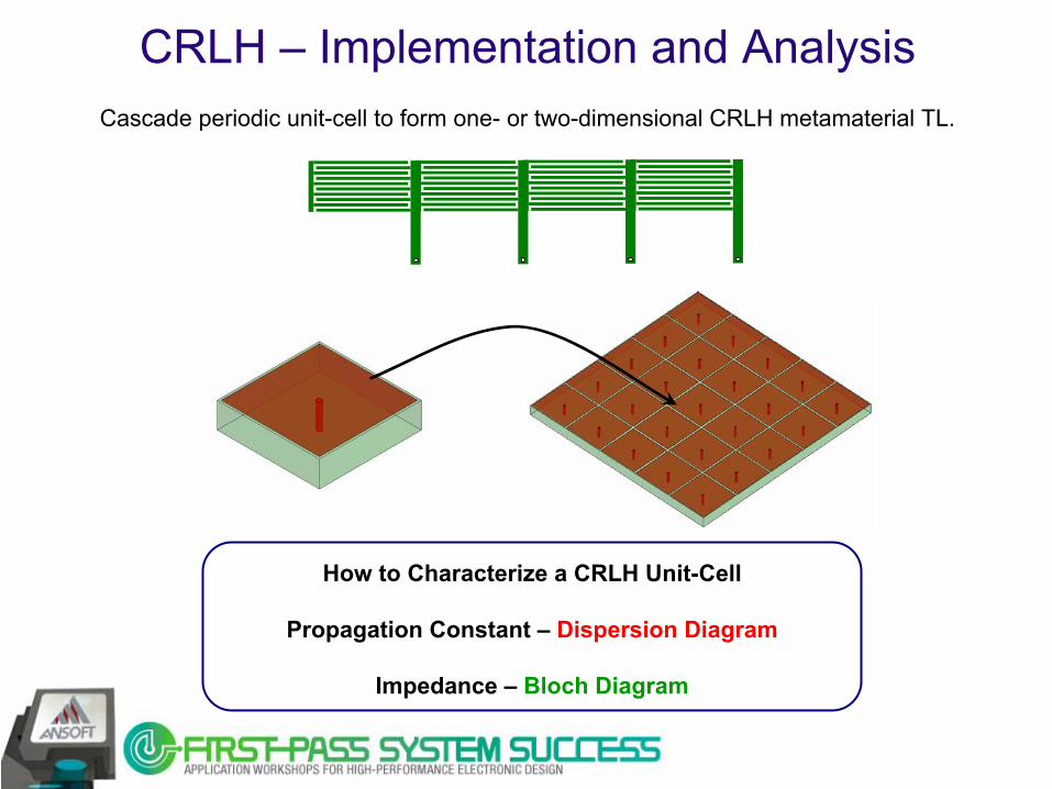
Cascade periodic unit-cell to form one-
or two-dimensional CRLH metamaterial TL.
How to Characterize a CRLH Unit-Cell
Propagation Constant –
Dispersion Diagram
Impedance –
Bloch Diagram
CRLH –
Implementation and Analysis
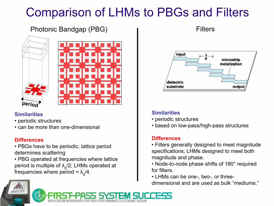
Comparison of LHMs to PBGs
and Filters
Similarities• periodic structures• can be more than one-dimensional
Differences•
PBGs
have to be periodic; lattice period determines scattering•
PBG operated at frequencies where lattice period is multiple of λg
/2; LHMs operated at frequencies where period < λg
/4.
periodSimilarities• periodic structures• based on low-pass/high-pass structures
Differences•
Filters generally designed to meet magnitude specifications; LHMs designed to meet both magnitude and phase.•
Node-to-node phase shifts of 180°
required for filters.•
LHMs can be one-, two-, or three-
dimensional and are used as bulk “mediums.”
Photonic Bandgap (PBG) Filters
Dominant-Mode Leaky Wave Antenna
Leaky-Wave Antenna TheoryPrinciple
source
0asin( ( ) )kθ β ω=
z
x
ko kzβ
kz2= ko
2-
β2
θ
β
ω0cβω −=
IVRH
GUIDANCE
IILH
RAD.
IIIRH
RAD.
0cβω +=
0ω
ILH
GUIDANCE
CRLHRH
Conventional RH Leaky-Wave Antenna(operated at higher-order mode)
CRLH Leaky-Wave Antenna [6](operated at dominant mode)
Characteristics:
•
Operating in leaky regions
II : BACKWARD ( β <
0 )
III : FORWARD ( β > 0 )
•
BROADSIDE
radiation ( β = 0
)
balanced
case: vg
(β = 0 ) ≠
0
• Fundamental mode
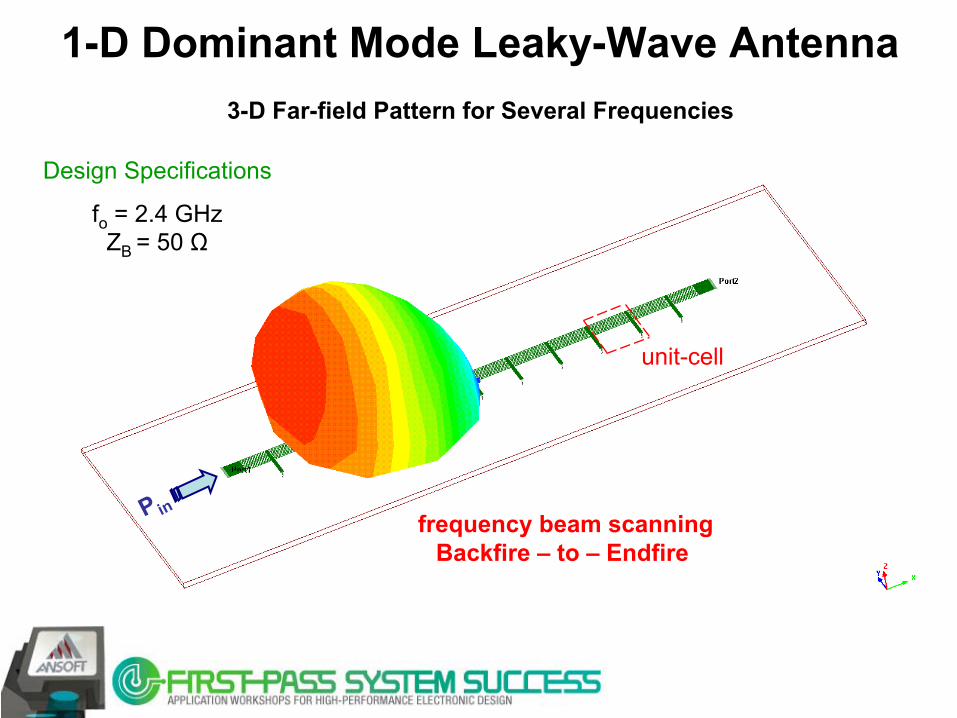
1-D Dominant Mode Leaky-Wave Antenna3-D Far-field Pattern for Several Frequencies
P infrequency beam scanning
Backfire –
to –
Endfire
unit-cell
Design Specifications
fo
= 2.4 GHzZB = 50 Ω
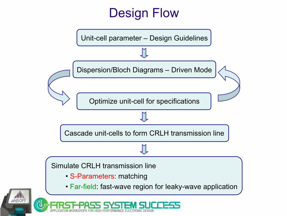
Design Flow
Unit-cell parameter –
Design Guidelines
Dispersion/Bloch Diagrams –
Driven Mode
Optimize unit-cell for specifications
Cascade unit-cells to form CRLH transmission line
Simulate CRLH transmission line• S-Parameters: matching• Far-field: fast-wave region for leaky-wave application
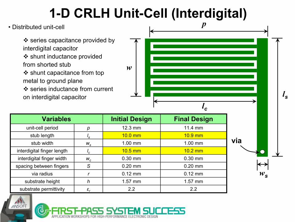
1-D CRLH Unit-Cell (Interdigital)
ls
p
lc
ws
w
via
Variables Initial Design Final Designunit-cell period p 12.3 mm 11.4 mm
stub length ls 10.0 mm 10.9 mmstub width ws 1.00 mm 1.00 mm
interdigital finger length lc 10.5 mm 10.2 mminterdigital finger width wc 0.30 mm 0.30 mm
spacing between fingers S 0.20 mm 0.20 mmvia radius r 0.12 mm 0.12 mm
substrate height h 1.57 mm 1.57 mmsubstrate permittivity εr 2.2 2.2
• Distributed unit-cell
series capacitance provided by interdigital capacitor
shunt inductance provided from shorted stub
shunt capacitance from top metal to ground plane
series inductance from current on interdigital capacitor
1-D CRLH Unit-Cell Design Guidelines*For 2-D space scanning, we need to design a balanced (ωse = ωsh
) CRLH unit-
cell so that there is a seamless transition from LH to RH operation.
1.
Choose center frequency, fo
, which represents broadside radiation. (fo
=2.4 GHz)
2.
Calculate width required to obtain Zo
, set w
to this value. (w~5.0 mm)
3.
Set stub width, ws
, to 20% of w. (ws
=1.0 mm)
4.
Set stub length (lsi=ls
-
w) to w; the electrical length of the stub has to be less than π/2.
mm 3.0
32
35
≈⎟⎠⎞
⎜⎝⎛ −
≈N
wwc
5.
Set the number of fingers, N, to 8 or 10. Then determine required wc
and S=2wc
/3. N=10 chosen.
6.
Calculate length of interdigital finger.
mm 5.10 88
≈≈≈ro
ogc f
clε
λ
mm 2.0=S
* Guidelines have been test on Rogers Duroid
5870 (er=2.33) and 5880 (er=2.2) for various substrate heights; for high permittivity substrate, the number of fingers should be reduced.
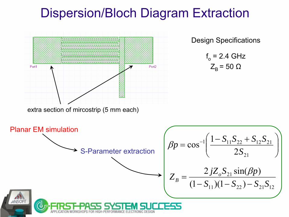
Dispersion/Bloch Diagram Extraction
extra section of mircostrip (5 mm each)
Planar EM simulation
S-Parameter extraction ⎟⎟⎠
⎞⎜⎜⎝
⎛ +−= −
21
211222111
21cos
SSSSSpβ
12212211
21
)1)(1()sin(2
SSSSpSjZZ o
B −−−=
β
Design Specifications
fo
= 2.4 GHzZB = 50 Ω
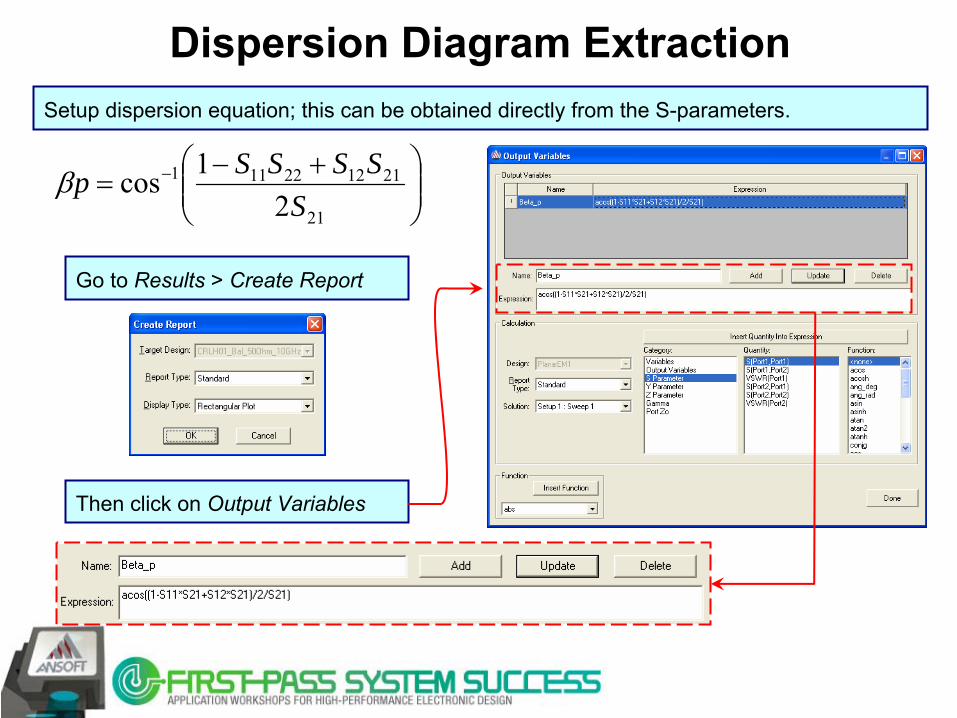
Dispersion Diagram ExtractionSetup dispersion equation; this can be obtained directly from the S-parameters.
⎟⎟⎠
⎞⎜⎜⎝
⎛ +−= −
21
211222111
21cos
SSSSSpβ
Go to Results > Create Report
Then click on Output Variables
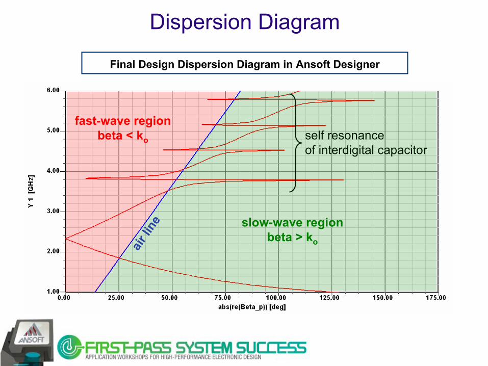
Dispersion Diagram
fast-wave regionbeta < ko
slow-wave regionbeta > koair
line
self resonance of interdigital capacitor
Final Design Dispersion Diagram in Ansoft Designer
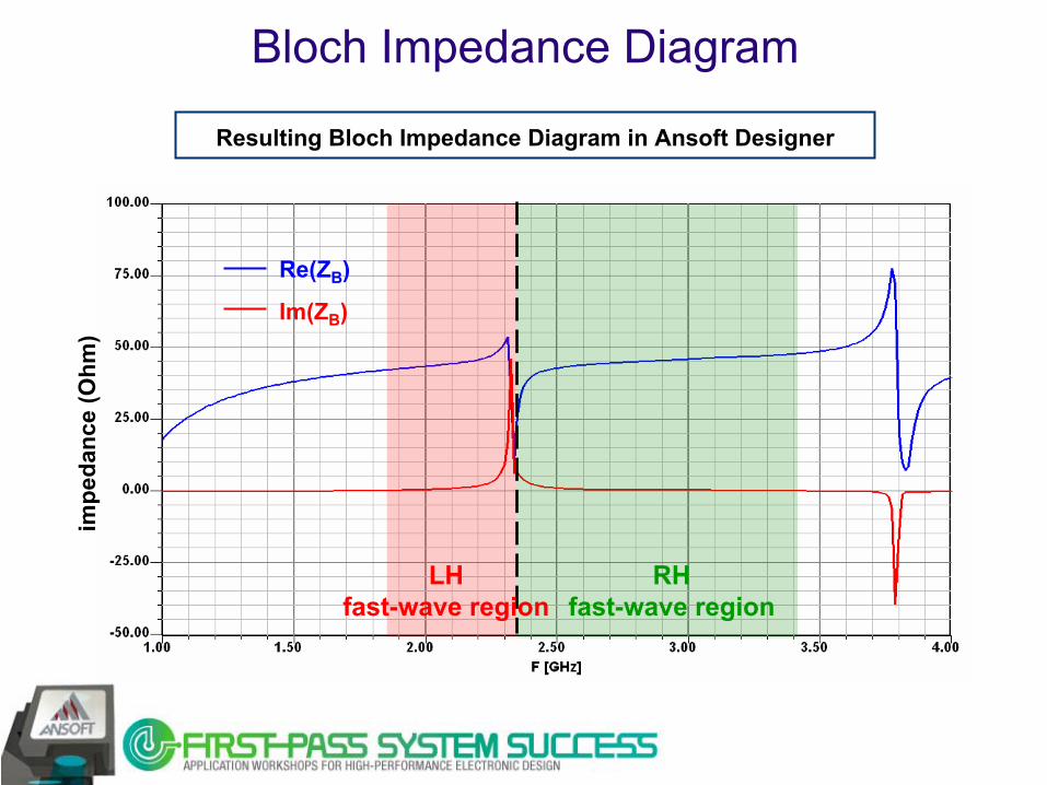
Bloch Impedance Diagram
RHfast-wave region
LHfast-wave region
Re(ZB
)
Im(ZB)
Resulting Bloch Impedance Diagram in Ansoft Designer
impe
danc
e (O
hm)
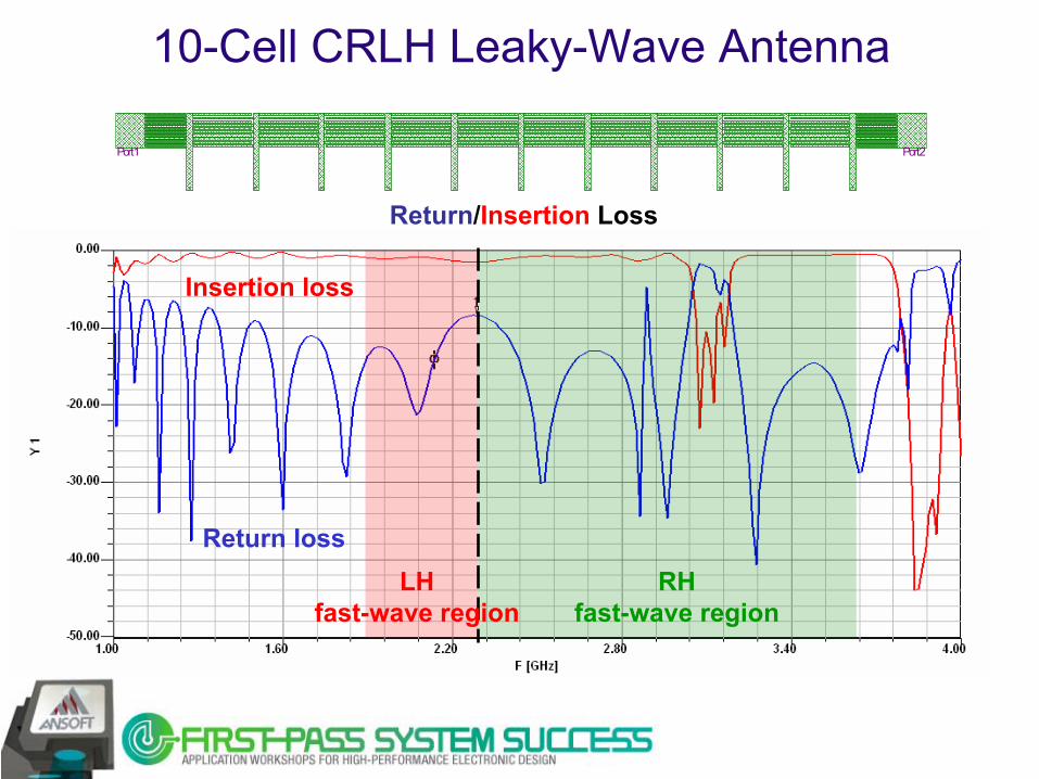
10-Cell CRLH Leaky-Wave Antenna
Port1 Port2
Insertion loss
Return lossRH
fast-wave regionLH
fast-wave region
Return/Insertion
Loss
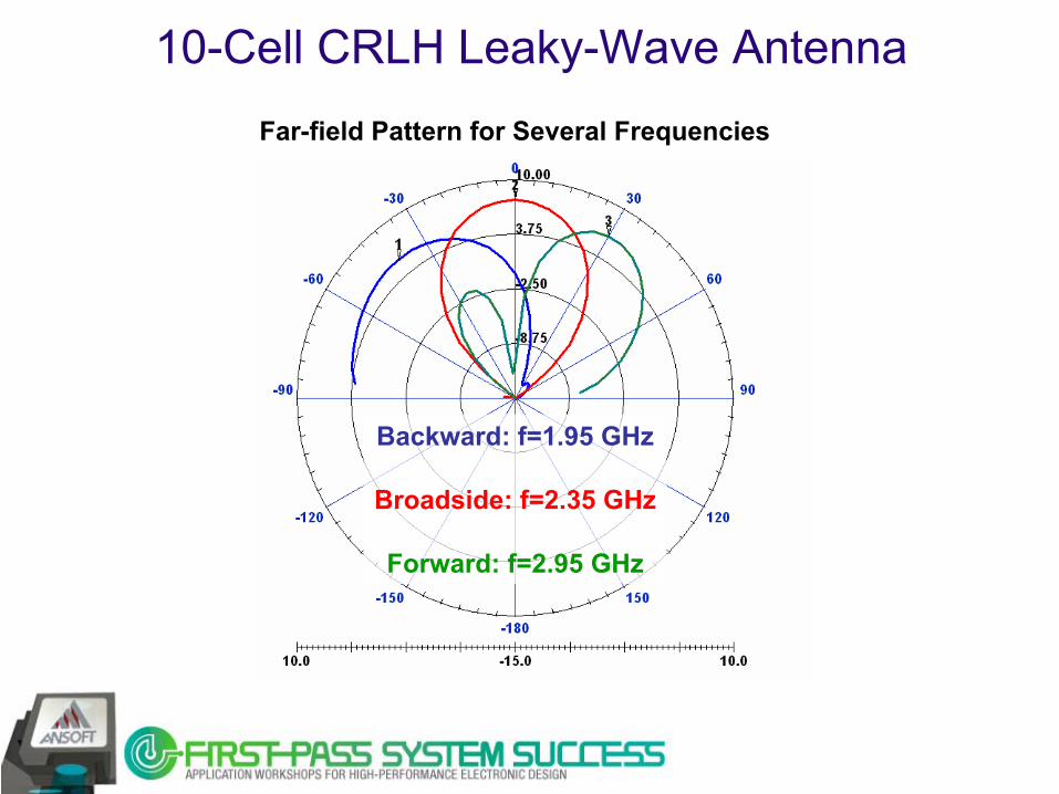
10-Cell CRLH Leaky-Wave AntennaFar-field Pattern for Several Frequencies
Backward: f=1.95 GHz
Broadside: f=2.35 GHz
Forward: f=2.95 GHz
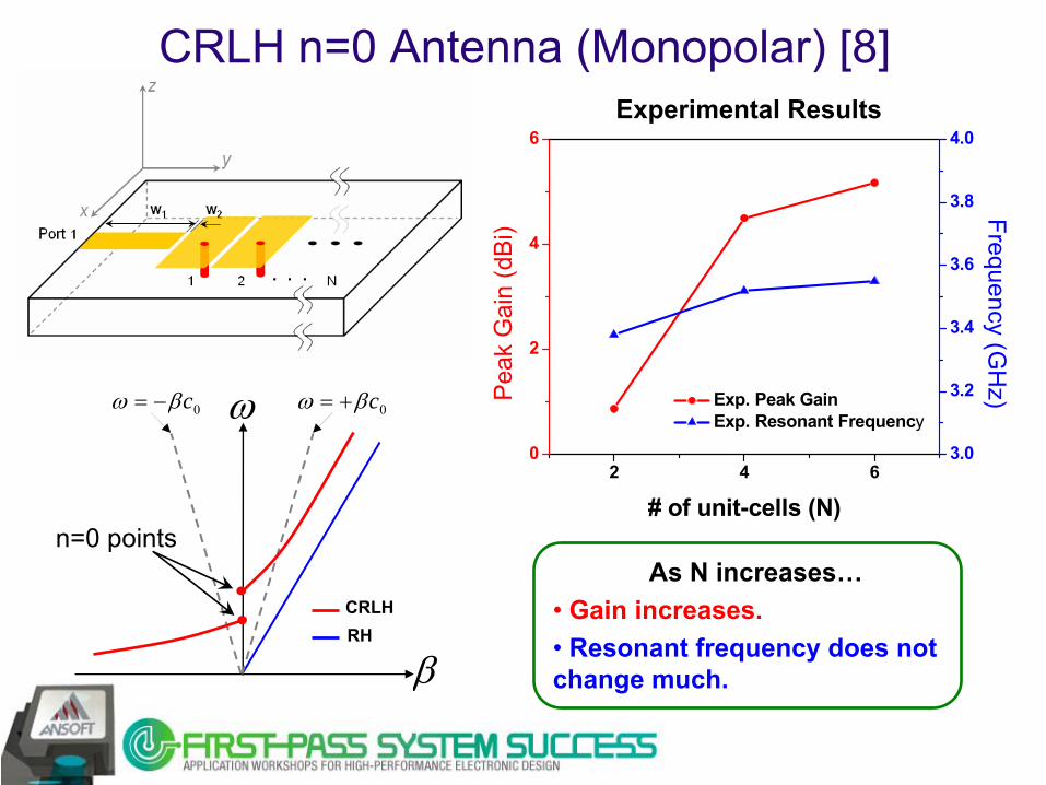
Small Metamaterial Antennas
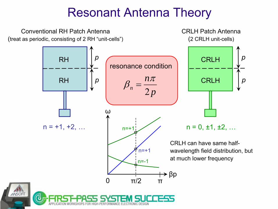
Resonant Antenna Theory
p
Conventional RH Patch Antenna(treat as periodic, consisting of 2 RH “unit-cells”)
CRLH Patch Antenna(2 CRLH unit-cells)
RH
RH
CRLH
CRLH
p
p
p
pn
n 2πβ =
resonance condition
n = +1, +2, … n = 0, ±1, ±2, …
ω
βp0 ππ/2
n=-1
n=+1
n=+1
CRLH can have same half-
wavelength field distribution, but at much lower frequency
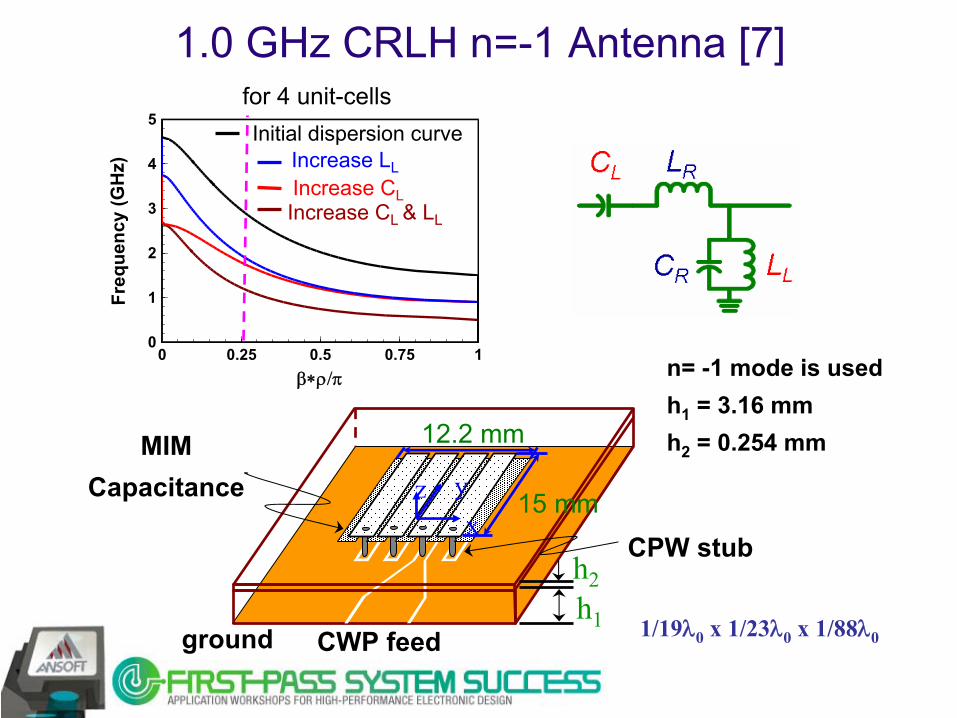
1.0 GHz CRLH n=-1 Antenna [7]
MIM Capacitance
ground
h2h1
CWP feed 1/19λ0
x 1/23λ0
x 1/88λ0
n= -1 mode is used h1
= 3.16 mmh2
= 0.254 mm
0 0.25 0.5 0.75 1β∗ρ/π
0
1
2
3
4
5Fr
eque
ncy
(GH
z)for 4 unit-cellsInitial dispersion curve
Increase LLIncrease CLIncrease CL & LL
15 mm
12.2 mm
xyz
CPW stub
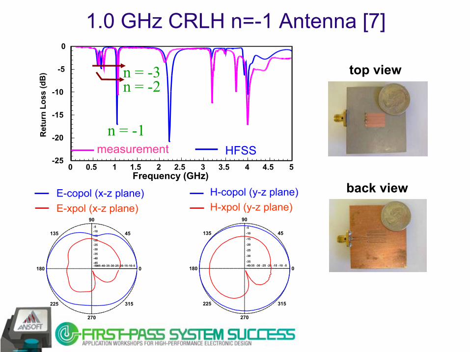
1.0 GHz CRLH n=-1 Antenna [7]
0 0.5 1 1.5 2 2.5 3 3.5 4 4.5 5Frequency (GHz)
-25
-20
-15
-10
-5
0R
etur
n Lo
ss (d
B)
n = -1
n = -2n = -3
measurement HFSS
0
45
90
135
180
225
270
315
-5
-5
-10
-10
-15
-15
-20
-20
-25
-25
-30
-30
-35
-35
-40
-40-45
-45-500
45
90
135
180
225
270
315
-5
-5
-10
-10
-15
-15
-20
-20
-25
-25
-30
-30-35
-35-40
E-copol
(x-z
plane)E-xpol
(x-z
plane)H-copol
(y-z
plane)H-xpol
(y-z
plane)
top view
back view
2 4 60
2
4
6
Exp. Peak Gain Exp. Resonant Frequency
# of unit-cells (N)P
eak
Gai
n (d
Bi)
3.0
3.2
3.4
3.6
3.8
4.0
Frequency (GH
z)
Experimental Results
As N increases…• Gain increases.•
Resonant frequency does not change much.
CRLH n=0 Antenna (Monopolar) [8]
β
ω0cβω −= 0cβω +=
CRLHRH
n=0 points
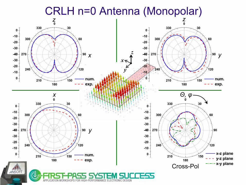
CRLH n=0 Antenna (Monopolar)
-40
-30
-20
-10
0
030
60
90
120
150180
210
240
270
300
330
-40
-30
-20
-10
0
num. exp.
x
y
Θ, φ
-40
-30
-20
-10
0
030
60
90
120
150180
210
240
270
300
330
-40
-30
-20
-10
0
x-z plane y-z plane x-y plane
-40
-30
-20
-10
0
030
60
90
120
150180
210
240
270
300
330
-40
-30
-20
-10
0
num. exp.
-40
-30
-20
-10
0
030
60
90
120
150180
210
240
270
300
330
-40
-30
-20
-10
0
num. exp.
zx
y
z
x
z
y
Cross-Pol
Dual-/Multi-Band Metamaterial Components
Characteristics:
• dual-band functionality for anarbitrary pair of frequencies f1
, f2
• principle:
transition frequency (fo
)provides DC offset
additional degreeof freedom with respect to thephase slope
• applications in multi-band systems
CRLH / CRLH hybrid [9]
CRLH
CRLH
CRLH CRLH
1 2
34
0
90−
180−
270−
360−
90
180
270
360
1fCRLH
2f conv2 13f f=
f
Conventional quadrature: restricted to odd
harmonics because only control on slope
conv. RHCRLH
DC offset
0f
Dual-Band Hybrid Coupler
Band # 1: 0.92 GHz
Band # 2: 1.74 GHz
0.6 0.8 1 1.2 1.4 1.6 1.8 2frequency (GHz)
-25
-20
-15
-10
-5
0
S-p
aram
eter
s (d
B)
S11S21S31S41
Experimental Results
2
1
1.89ff=
LHTLs
0Z 0Z0
2Z
0
2Z
Branch Linein
isolated out
out
Dual-Band Hybrid Coupler
Negative Refractive Index Lenses
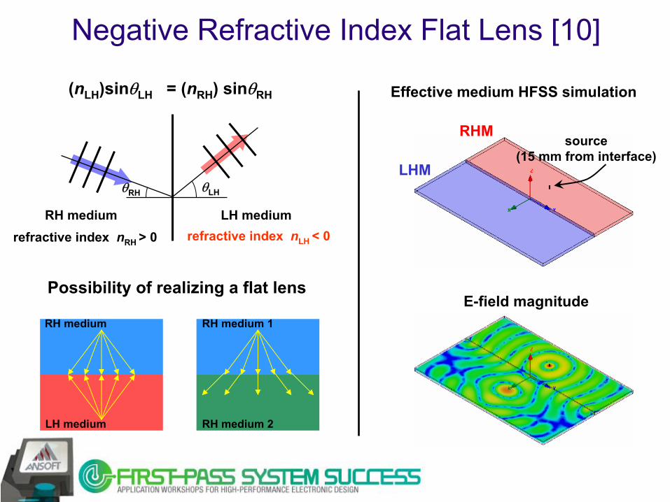
(nLH
)sinθLH
= (nRH
) sinθRH
RH medium LH medium
θRH θLH
refractive index nRH
> 0 refractive index nLH
< 0
Possibility of realizing a flat lens
RH medium
LH medium
RH medium 1
RH medium 2
source(15 mm from interface)
LHM
RHM
E-field magnitude
Effective medium HFSS simulation
Negative Refractive Index Flat Lens [10]
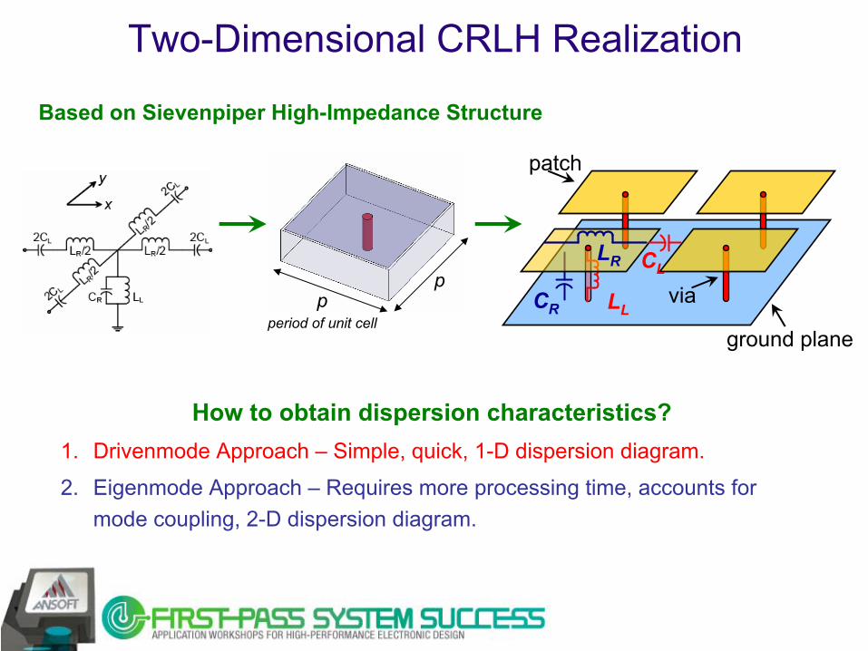
pperiod of unit cell
pCL
LR
CR LL
patch
ground plane
via
Based on Sievenpiper High-Impedance Structure
Two-Dimensional CRLH Realization
How to obtain dispersion characteristics?1.
Drivenmode
Approach –
Simple, quick, 1-D dispersion diagram.
2.
Eigenmode
Approach –
Requires more processing time, accounts for mode coupling, 2-D dispersion diagram.
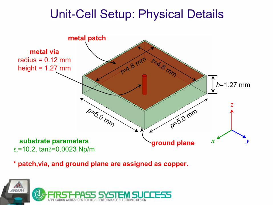
Unit-Cell Setup: Physical Details
substrate parametersεr
=10.2, tanδ=0.0023 Np/mx y
z
h=1.27 mm
t=4.8 mm t=4.8 mm
p=5.0 mm p=5.0 mm
metal patch
metal viaradius = 0.12 mmheight = 1.27 mm
ground plane
* patch,via, and ground plane are assigned as copper.
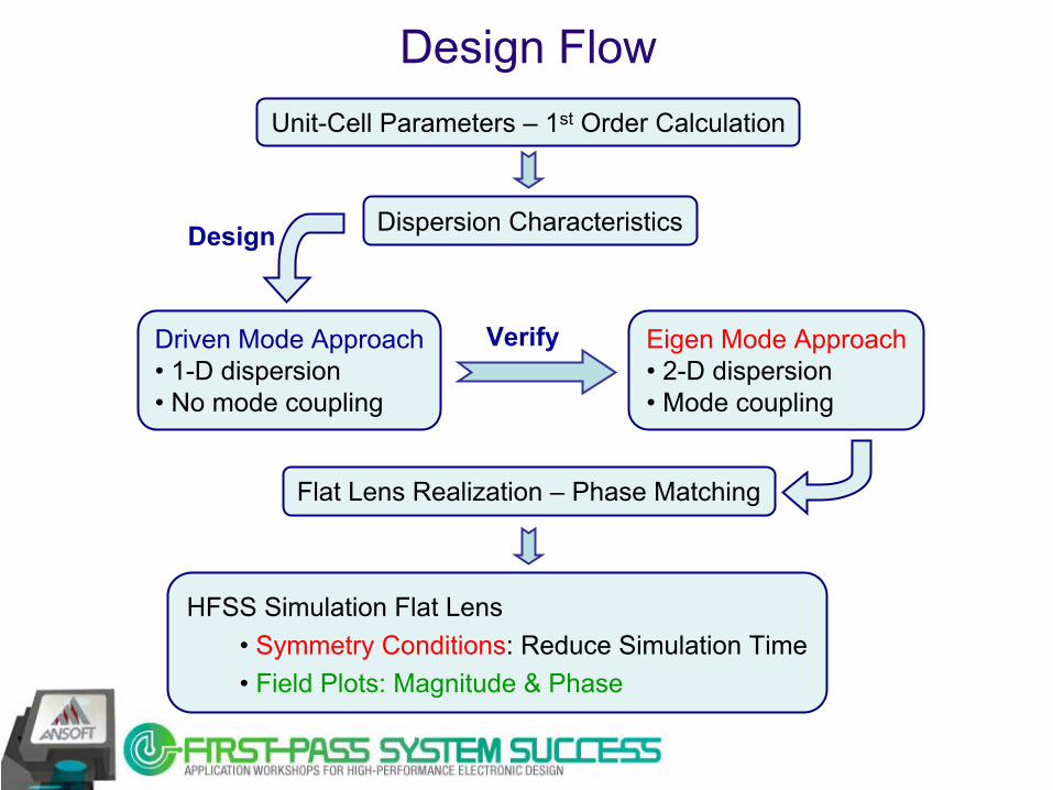
Design FlowUnit-Cell Parameters –
1st
Order Calculation
Dispersion Characteristics
HFSS Simulation Flat Lens • Symmetry Conditions: Reduce Simulation Time• Field Plots: Magnitude & Phase
Driven Mode Approach• 1-D dispersion• No mode coupling
Eigen Mode Approach• 2-D dispersion• Mode coupling
Design
Verify
Flat Lens Realization –
Phase Matching
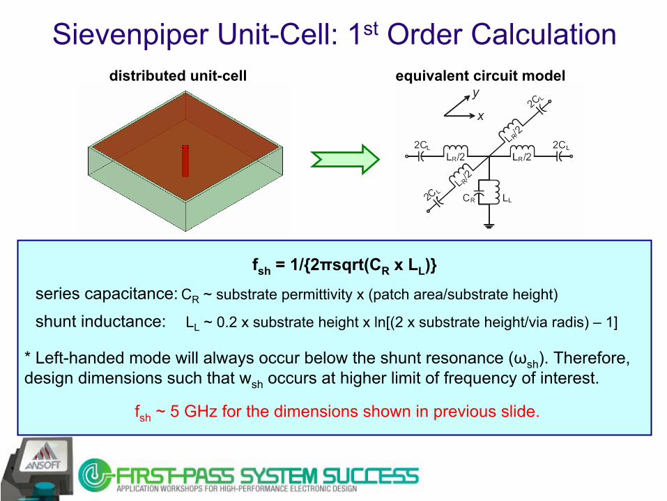
Sievenpiper Unit-Cell: 1st
Order Calculation
distributed unit-cell equivalent circuit model
series capacitance: CR
~ substrate permittivity x (patch area/substrate height)
shunt inductance: LL
~ 0.2 x substrate height x ln[(2 x substrate height/via radis) –
1]
fsh
= 1/2πsqrt(CR
x LL
)
* Left-handed mode will always occur below the shunt resonance (ωsh
). Therefore, design dimensions such that wsh
occurs at higher limit of frequency of interest.
fsh
~ 5 GHz for the dimensions shown in previous slide.
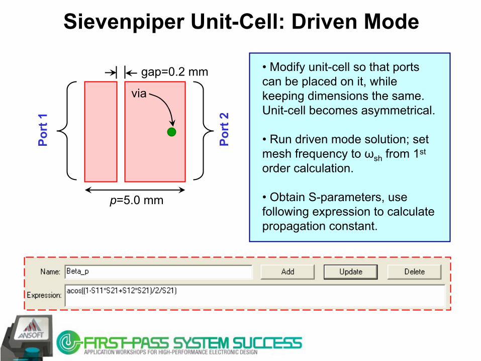
Sievenpiper Unit-Cell: Driven Mode
p=5.0 mm
gap=0.2 mm
via
Port
1
Port
2
•
Modify unit-cell so that ports can be placed on it, while keeping dimensions the same. Unit-cell becomes asymmetrical.
•
Run driven mode solution; set mesh frequency to ωsh
from 1st
order calculation.
•
Obtain S-parameters, use following expression to calculate propagation constant.
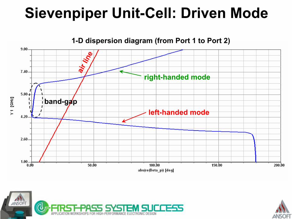
Sievenpiper Unit-Cell: Driven Mode
left-handed mode
right-handed mode
band-gap
air l
ine
1-D dispersion diagram (from Port 1 to Port 2)
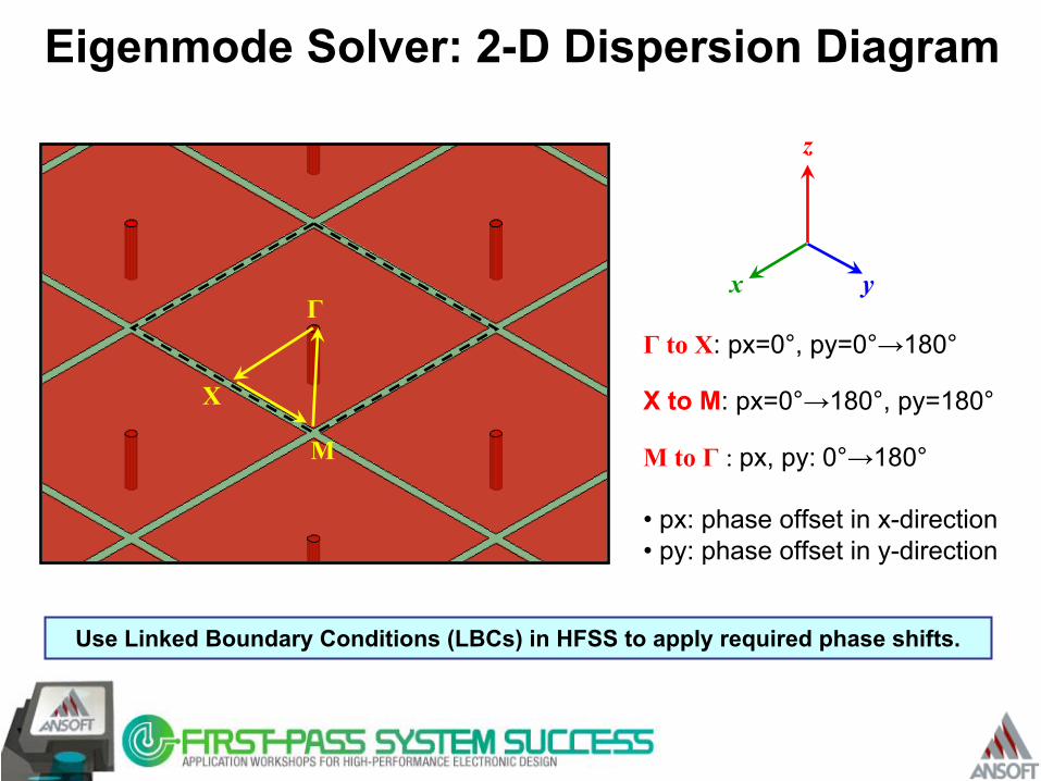
Eigenmode Solver: 2-D Dispersion Diagram
Γ
X
M
x y
z
Γ
to X: px=0°, py=0°→180°
X to M: px=0°→180°, py=180°
M to Γ
: px, py:
0°→180°
• px: phase offset in x-direction• py: phase offset in y-direction
Use Linked Boundary Conditions (LBCs) in HFSS to apply required phase shifts.
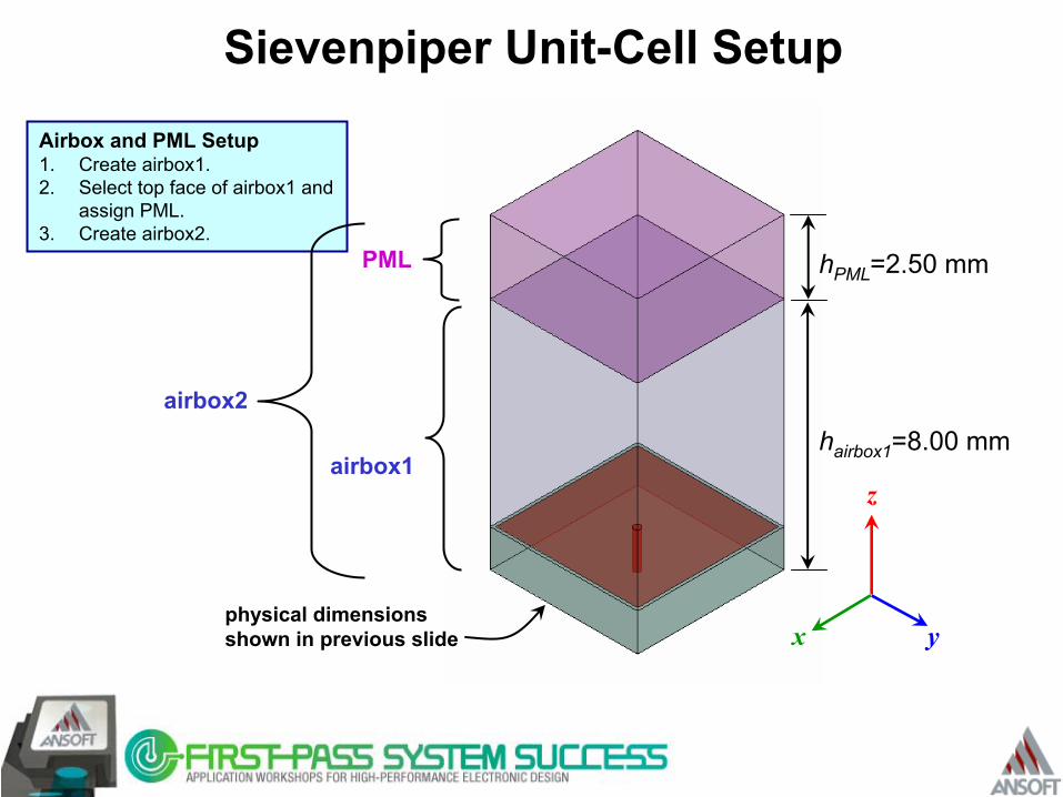
airbox1
airbox2
x y
z
hairbox1
=8.00 mm
hPML
=2.50 mm
Sievenpiper Unit-Cell Setup
Airbox
and PML Setup1.
Create airbox1.2.
Select top face of airbox1 and assign PML.
3.
Create airbox2.PML
physical dimensions shown in previous slide
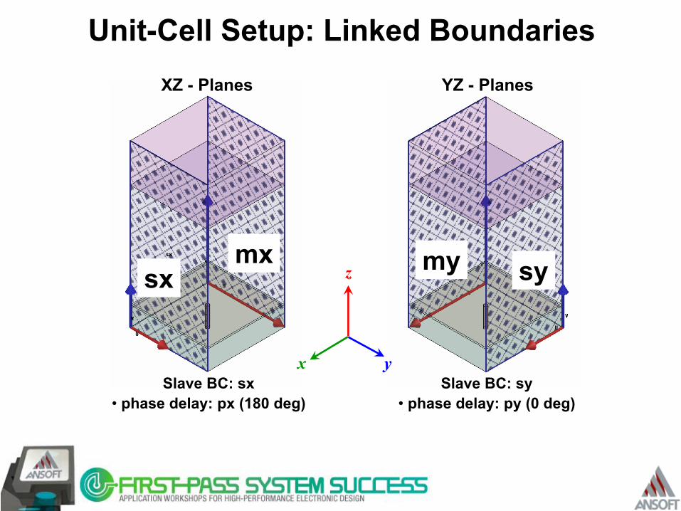
Unit-Cell Setup: Linked BoundariesXZ -
Planes
Slave BC: sx• phase delay: px (180 deg)
YZ -
Planes
mxsx my sy
Slave BC: sy• phase delay: py (0 deg)
x y
z
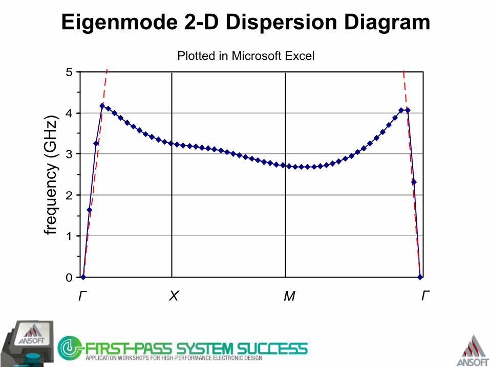
Eigenmode
2-D Dispersion Diagram
0
1
2
3
4
5
Γ X M Γ
frequ
ency
(GH
z)Plotted in Microsoft Excel
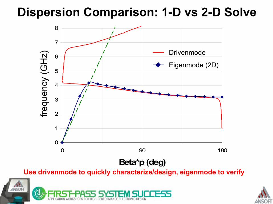
Dispersion Comparison: 1-D vs
2-D Solve
0
1
2
3
4
5
6
7
8
0 90 180
Beta*p (deg)
frequ
ency
(GH
z) Drivenmode
Eigenmode (2D)
Use drivenmode
to quickly characterize/design, eigenmode
to verify
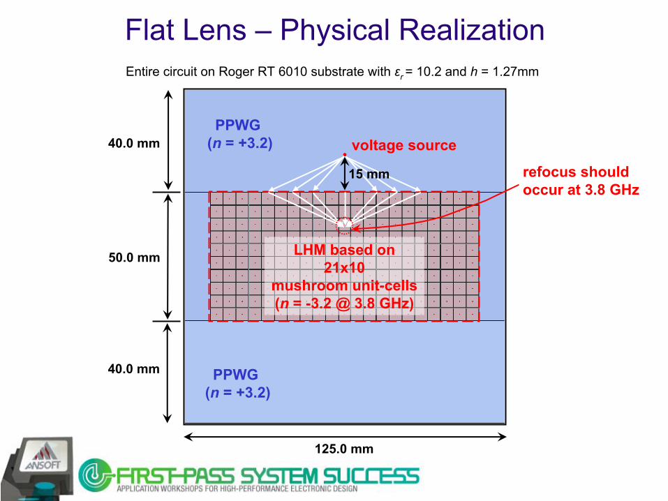
Flat Lens –
Physical RealizationEntire circuit on Roger RT 6010 substrate with εr = 10.2 and h = 1.27mm
voltage source
LHM based on21x10
mushroom unit-cells(n
= -3.2 @ 3.8 GHz)
PPWG (n
= +3.2)
PPWG (n
= +3.2)
15 mm refocus shouldoccur at 3.8 GHz
40.0 mm
50.0 mm
40.0 mm
125.0 mm
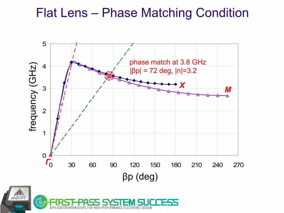
Flat Lens –
Phase Matching Condition
0
1
2
3
4
5
0 30 60 90 120 150 180 210 240 270
phase match at 3.8 GHz|βp| = 72 deg, |n|=3.2
Γ
X M
βp (deg)
frequ
ency
(GH
z)
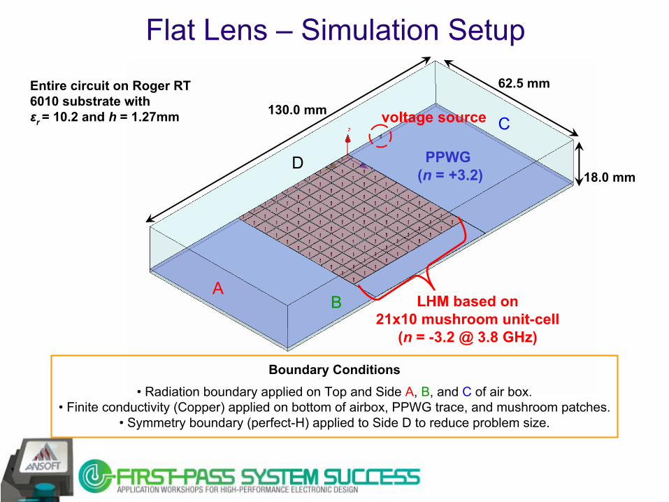
PPWG (n
= +3.2)
LHM based on21x10 mushroom unit-cell
(n
= -3.2 @ 3.8 GHz)
130.0 mm
62.5 mm
18.0 mm
AB
C
D
Entire circuit on Roger RT 6010 substrate withεr = 10.2 and h = 1.27mm
Boundary Conditions• Radiation boundary applied on Top and Side A, B, and C
of air box.• Finite conductivity (Copper) applied on bottom of airbox, PPWG trace, and mushroom patches.
• Symmetry boundary (perfect-H) applied to Side D to reduce problem size.
Flat Lens –
Simulation Setup
voltage source
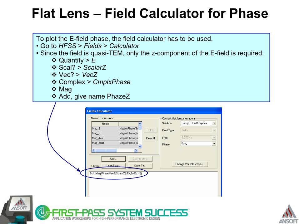
Flat Lens –
Field Calculator for Phase
To plot the E-field phase, the field calculator has to be used. • Go to HFSS > Fields > Calculator• Since the field is quasi-TEM, only the z-component of the E-field is required.
Quantity > EScal? > ScalarZVec? > VecZComplex > CmplxPhaseMagAdd, give name PhazeZ
Flat Lens –
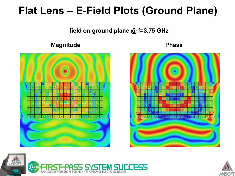
E-Field Plots (Ground Plane)
field on ground plane @ f=3.75 GHz
Magnitude Phase
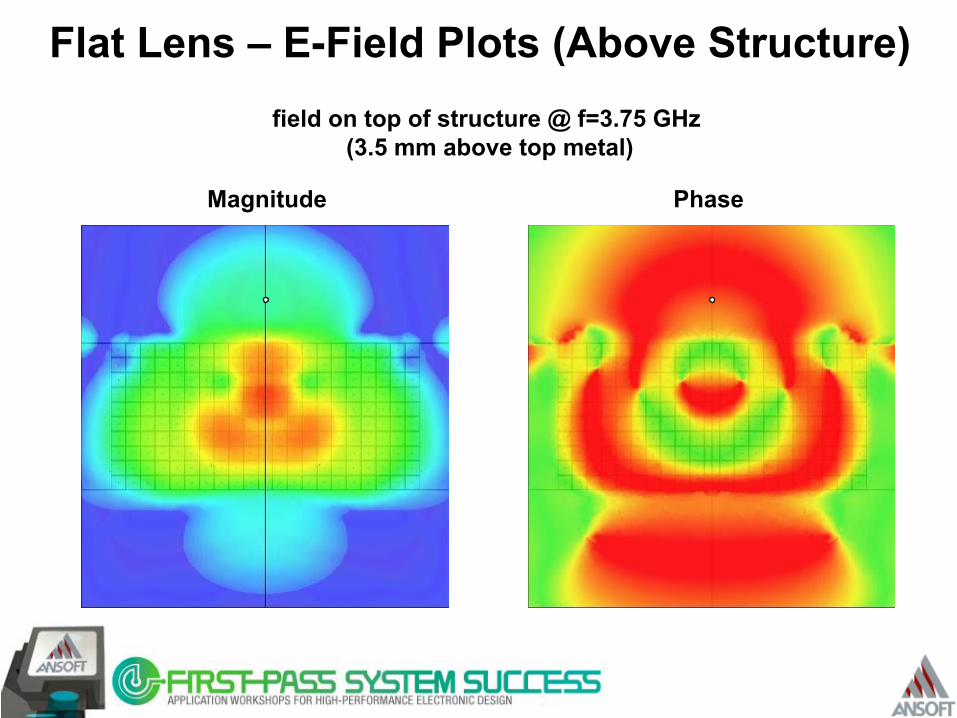
Flat Lens –
E-Field Plots (Above Structure)field on top of structure @ f=3.75 GHz
(3.5 mm above top metal)
Magnitude Phase
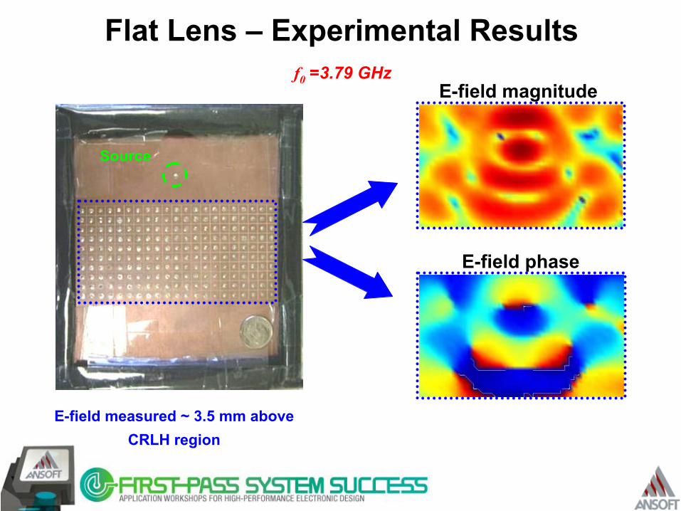
Flat Lens –
Experimental Results
SourceSource
E-field magnitude
E-field phase
E-field measured ~ 3.5 mm above CRLH region
f0
=3.79 GHz

Future Trends
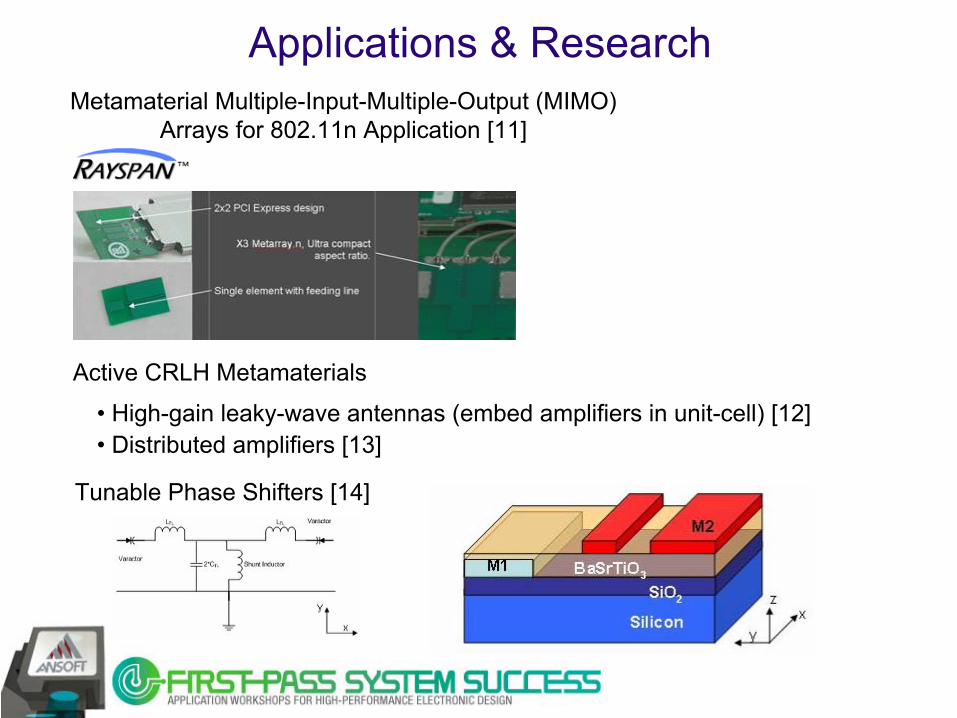
Applications & ResearchMetamaterial Multiple-Input-Multiple-Output (MIMO)
Arrays for 802.11n Application [11]
Active CRLH Metamaterials
• High-gain leaky-wave antennas (embed amplifiers in unit-cell) [12]• Distributed amplifiers [13]
Tunable Phase Shifters [14]
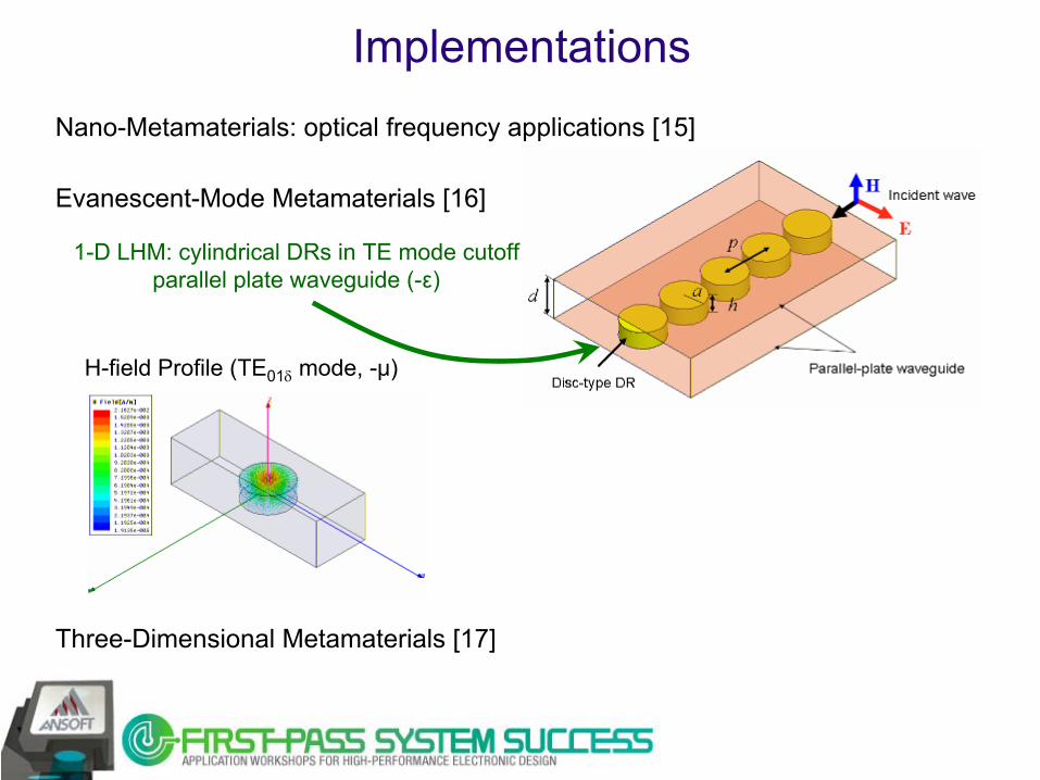
ImplementationsNano-Metamaterials: optical frequency applications [15]
1-D LHM: cylindrical DRs
in TE mode cutoff parallel plate waveguide (-ε)
Evanescent-Mode Metamaterials [16]
H-field Profile (TE01δ
mode, -μ)
Three-Dimensional Metamaterials [17]
Summary• Left-Handed Metamaterial Introduction
Resonant approachTransmission line approach
• Composite Right/Left-Handed Metamaterial• Metamaterial-Based Microwave Devices
Dominant leaky-wave antennaSmall, resonant backward wave antennasDual-band hybrid couplerNegative refractive index flat lens
• Future Trends
References1)
C. Caloz, C.C. Chang, and T. Itoh, “’Full-wave verification of the fundamental properties of left-handed materials (LHMs) in waveguide configurations,” J. App. Phys., vol. 90, no. 11, pp. 5483-5486, Dec. 2001.
2)
R.A. Shelby, D.R. Smith, and S. Schultz, “Experimental verification of a negative index of refraction,” Science, vol. 292, pp. 77-79, Apr. 2001.
3)
A. Lai, C. Caloz, and T. Itoh, “Composite right/left-handed transmission line metamaterials,” IEEE Microwave Magazine, Vol. 5, no. 3, pp. 34-50, Sep. 2004.
4)
C. Caloz and T. Itoh, Electromagnetic Metamaterials: Transmission Line Theory and Microwave Applications, Wiley and IEEE Press, Hoboken, NJ, 2005.
5)
D. Sievenpiper, L. Zhang, R.F.J. Broas, N.G. Alexopolous, and E. Yablonovitch, “High-impedance surface electromagnetic surfaces with a forbidden frequency band,” IEEE Trans. Microwave Theory Tech., vol. 47, no. 11, pp. 2059-2074, Nov. 1999.
6)
L. Liu, C. Caloz, and T. Itoh, “Dominant mode (DM) leaky-wave antenna with backfire-to-endfire
scanning capability,” Electron. Lett., vol. 38, no. 23. pp. 1414-1416, Nov. 2002.
7)
C.J. Lee, K.M.K.H. Leong, and T. Itoh, “Design of resonant small
antenna using composite right/left-handed transmission line,” Proc. IEEE Antennas and Propagation Society Int. Symp., Washington D.C., Jun. 2005.
8)
A. Lai, K.M.K.H. Leong, and T. Itoh, “Infinite wavelength resonant antennas with monopolar radiation patterns based on periodic structures,” IEEE Trans. Antennas Propag.,
vol. 55, no. 3, pp. 868-876, Mar. 2007.9)
I. Lin, C. Caloz, and T. Itoh, “A branch-line coupler with two arbitrary operating frequencies using left-handed transmission lines,” IEEE-MTT Int. Symp. Dig., Philadelphia, PA, Jun. 2003, vol. 1, pp. 325–327.
10)
A. Lai, “Theory and design of composite right/left-handed metamaterial-based microwave lenses," Master Thesis, Dept. E. E., UCLA, Los Angeles, CA, 2005.
11)
Rayspan
Corporation, http://www.rayspan.com12)
F. P. Casares-Miranda, C. Camacho Peñalosa, and C. Caloz, “High-gain active composite right/left-handed leaky-wave antenna,” IEEE Trans. Antennas Propag., vol. 54, no. 8, pp. 2292-2300, Aug. 2006.
13)
J. Mata-Conteras, T. M. Martìn-Guerrero, and C. Camacho-Peñalosa, “Distributed amplifiers with composite right/left-handed transmission lines,” Microwave Opt. Technol. Lett., vol. 48, no. 3, pp. 609-613, March 2006.
14)
E.S. Ash, “Continuous phase shifter using ferroelectric varactors
and composite right-left handed transmission lines,” Master Thesis, Dept. E.E., UCLA, Los Angeles, CA 2006.
15)
V.A. Podolskiy, A.K. Sarychev, and V.M. Shalaev, “Plasmon modes in metal nanowires
and left-handed materials,” J. Nonlin. Opt. Phys. Mat., vol. 11, no. 1, pp. 65-74, 2002.
16)
T. Ueda, A. Lai, and T. Itoh, “Demonstration of negative refraction in a cutoff parallel-plate waveguide loaded with 2-D square lattice of dielectric resonators,” IEEE Trans. Microwave Theory Tech., vol. 55, no. 6, pp. 1280-1287, Jun. 2007.
17)
M. Zedler, P. Russer, and C. Caloz, “Circuital and experimental demonstration of a 3D isotropic LH metamaterial based on the rotated TLM scheme,” IEEE-MTT Int'l Symp., Honolulu, HI, Jun. 2007.
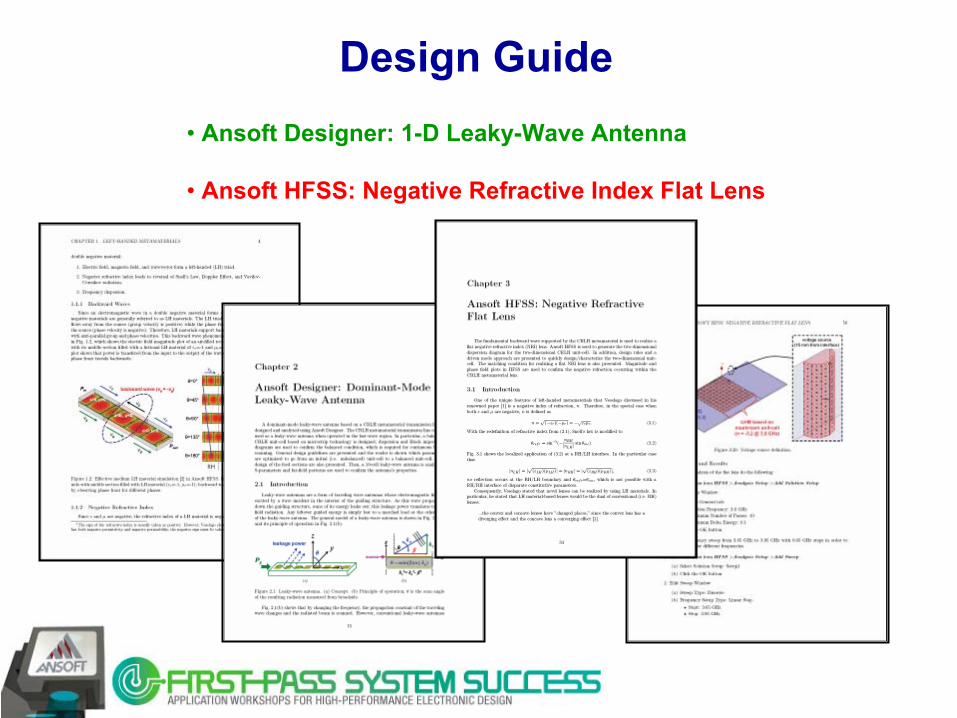
Design Guide• Ansoft Designer: 1-D Leaky-Wave Antenna
• Ansoft HFSS: Negative Refractive Index Flat Lens
专注于微波、射频、天线设计人才的培养 易迪拓培训 网址:http://www.edatop.com
H F S S 视 频 培 训 课 程 推 荐
HFSS 软件是当前最流行的微波无源器件和天线设计软件,易迪拓培训(www.edatop.com)是国内
最专业的微波、射频和天线设计培训机构。
为帮助工程师能够更好、更快地学习掌握 HFSS 的设计应用,易迪拓培训特邀李明洋老师主讲了
多套 HFSS 视频培训课程。李明洋老师具有丰富的工程设计经验,曾编著出版了《HFSS 电磁仿真设计
应用详解》、《HFSS 天线设计》等多本 HFSS 专业图书。视频课程,专家讲解,直观易学,是您学习
HFSS 的最佳选择。
HFSS 学习培训课程套装
该套课程套装包含了本站全部 HFSS 培训课程,是迄今国内最全面、最
专业的HFSS培训教程套装,可以帮助您从零开始,全面深入学习HFSS
的各项功能和在多个方面的工程应用。购买套装,更可超值赠送 3 个月
免费学习答疑,随时解答您学习过程中遇到的棘手问题,让您的 HFSS
学习更加轻松顺畅…
课程网址:http://www.edatop.com/peixun/hfss/11.html
HFSS 天线设计培训课程套装
套装包含 6 门视频课程和 1 本图书,课程从基础讲起,内容由浅入深,
理论介绍和实际操作讲解相结合,全面系统的讲解了 HFSS 天线设计
的全过程。是国内最全面、最专业的 HFSS 天线设计课程,可以帮助
您快速学习掌握如何使用 HFSS 设计天线,让天线设计不再难…
课程网址:http://www.edatop.com/peixun/hfss/122.html
更多 HFSS 视频培训课程:
两周学会 HFSS —— 中文视频培训课程
课程从零讲起,通过两周的课程学习,可以帮助您快速入门、自学掌握 HFSS,是 HFSS 初学者
的最好课程,网址:http://www.edatop.com/peixun/hfss/1.html
HFSS 微波器件仿真设计实例 —— 中文视频教程
HFSS 进阶培训课程,通过十个 HFSS 仿真设计实例,带您更深入学习 HFSS 的实际应用,掌握
HFSS 高级设置和应用技巧,网址:http://www.edatop.com/peixun/hfss/3.html
HFSS 天线设计入门 —— 中文视频教程
HFSS 是天线设计的王者,该教程全面解析了天线的基础知识、HFSS 天线设计流程和详细操作设
置,让 HFSS 天线设计不再难,网址:http://www.edatop.com/peixun/hfss/4.html
更多 HFSS 培训课程,敬请浏览:http://www.edatop.com/peixun/hfss
`
专注于微波、射频、天线设计人才的培养 易迪拓培训 网址:http://www.edatop.com
关于易迪拓培训:
易迪拓培训(www.edatop.com)由数名来自于研发第一线的资深工程师发起成立,一直致力和专注
于微波、射频、天线设计研发人才的培养;后于 2006 年整合合并微波 EDA 网(www.mweda.com),
现已发展成为国内最大的微波射频和天线设计人才培养基地,成功推出多套微波射频以及天线设计相
关培训课程和 ADS、HFSS 等专业软件使用培训课程,广受客户好评;并先后与人民邮电出版社、电
子工业出版社合作出版了多本专业图书,帮助数万名工程师提升了专业技术能力。客户遍布中兴通讯、
研通高频、埃威航电、国人通信等多家国内知名公司,以及台湾工业技术研究院、永业科技、全一电
子等多家台湾地区企业。
我们的课程优势:
※ 成立于 2004 年,10 多年丰富的行业经验
※ 一直专注于微波射频和天线设计工程师的培养,更了解该行业对人才的要求
※ 视频课程、既能达到现场培训的效果,又能免除您舟车劳顿的辛苦,学习工作两不误
※ 经验丰富的一线资深工程师讲授,结合实际工程案例,直观、实用、易学
联系我们:
※ 易迪拓培训官网:http://www.edatop.com
※ 微波 EDA 网:http://www.mweda.com
※ 官方淘宝店:http://shop36920890.taobao.com
专注于微波、射频、天线设计人才的培养
官方网址:http://www.edatop.com 易迪拓培训 淘宝网店:http://shop36920890.taobao.com