
Photocathode 1.5 (1, 3.5) cell superconducting RF gun with electric and magnetic RF focusing

1.1 LOW FREQUENCY PARAMETERS:
UNIT -1
TWO PORT RF NETWORK THEORY
Fatima Michael College of Engineering & Technology
Fatima Michael College of Engineering & Technology
Fatima Michael College of Engineering & Technologywww.studentsfocus.com
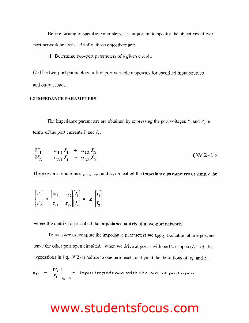
1.2 IMPEDANCE PARAMETERS:
Fatima Michael College of Engineering & Technology
Fatima Michael College of Engineering & Technology
Fatima Michael College of Engineering & Technologywww.studentsfocus.com
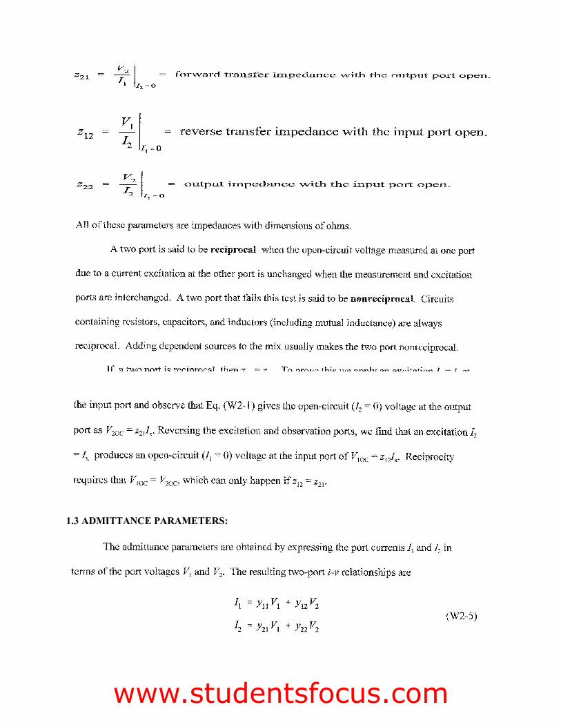
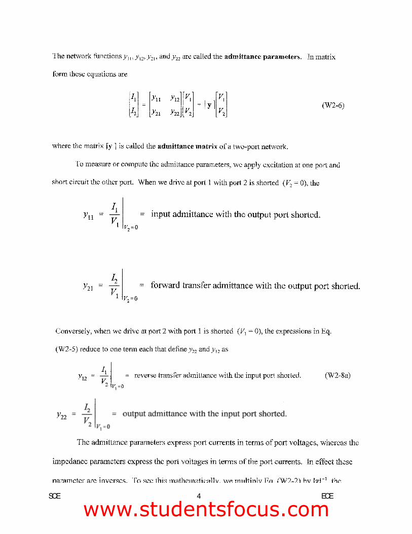
1.3 ADMITTANCE PARAMETERS:
Fatima Michael College of Engineering & Technology
Fatima Michael College of Engineering & Technology
Fatima Michael College of Engineering & Technologywww.studentsfocus.com
SCE 4 ECE
Fatima Michael College of Engineering & Technology
Fatima Michael College of Engineering & Technology
Fatima Michael College of Engineering & Technologywww.studentsfocus.com
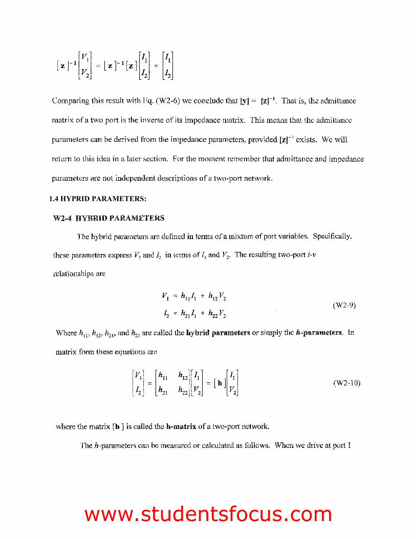
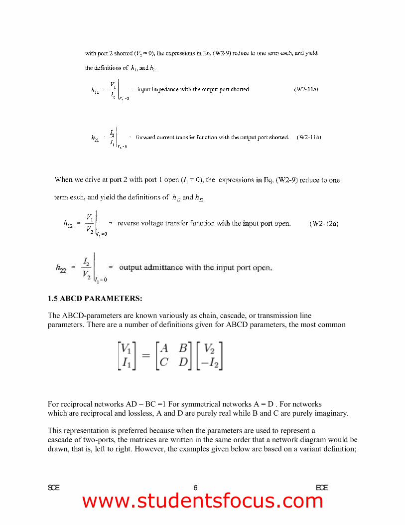
1.4 HYPRID PARAMETERS:
Fatima Michael College of Engineering & Technology
Fatima Michael College of Engineering & Technology
Fatima Michael College of Engineering & Technologywww.studentsfocus.com
SCE 6 ECE
1.5 ABCD PARAMETERS:
The ABCD-parameters are known variously as chain, cascade, or transmission line parameters. There are a number of definitions given for ABCD parameters, the most common
For reciprocal networks AD – BC =1 For symmetrical networks A = D . For networks which are reciprocal and lossless, A and D are purely real while B and C are purely imaginary.
This representation is preferred because when the parameters are used to represent a cascade of two-ports, the matrices are written in the same order that a network diagram would be drawn, that is, left to right. However, the examples given below are based on a variant definition;
Fatima Michael College of Engineering & Technology
Fatima Michael College of Engineering & Technology
Fatima Michael College of Engineering & Technologywww.studentsfocus.com
EC2403 RF &MICROWAVE ENGINEERING
SCE 7 ECE
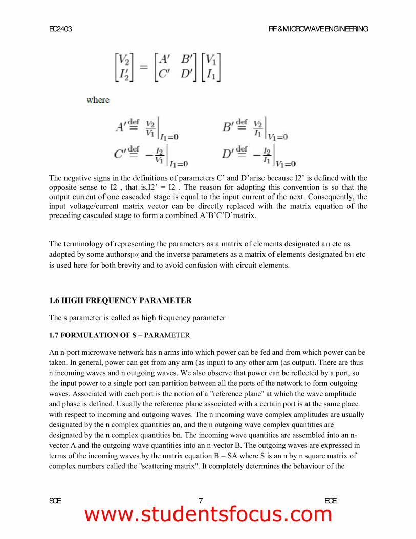
The negative signs in the definitions of parameters C’ and D’arise because I2’ is defined with the opposite sense to I2 , that is,I2’ = I2 . The reason for adopting this convention is so that the output current of one cascaded stage is equal to the input current of the next. Consequently, the input voltage/current matrix vector can be directly replaced with the matrix equation of the preceding cascaded stage to form a combined A’B’C’D’matrix. The terminology of representing the parameters as a matrix of elements designated a11 etc as adopted by some authors[10] and the inverse parameters as a matrix of elements designated b11 etc is used here for both brevity and to avoid confusion with circuit elements.
1.6 HIGH FREQUENCY PARAMETER
The s parameter is called as high frequency parameter
1.7 FORMULATION OF S – PARAMETER
An n-port microwave network has n arms into which power can be fed and from which power can be taken. In general, power can get from any arm (as input) to any other arm (as output). There are thus n incoming waves and n outgoing waves. We also observe that power can be reflected by a port, so the input power to a single port can partition between all the ports of the network to form outgoing waves. Associated with each port is the notion of a "reference plane" at which the wave amplitude and phase is defined. Usually the reference plane associated with a certain port is at the same place with respect to incoming and outgoing waves. The n incoming wave complex amplitudes are usually designated by the n complex quantities an, and the n outgoing wave complex quantities are designated by the n complex quantities bn. The incoming wave quantities are assembled into an n-vector A and the outgoing wave quantities into an n-vector B. The outgoing waves are expressed in terms of the incoming waves by the matrix equation B = SA where S is an n by n square matrix of complex numbers called the "scattering matrix". It completely determines the behaviour of the
Fatima Michael College of Engineering & Technology
Fatima Michael College of Engineering & Technology
Fatima Michael College of Engineering & Technologywww.studentsfocus.com
EC2403 RF &MICROWAVE ENGINEERING
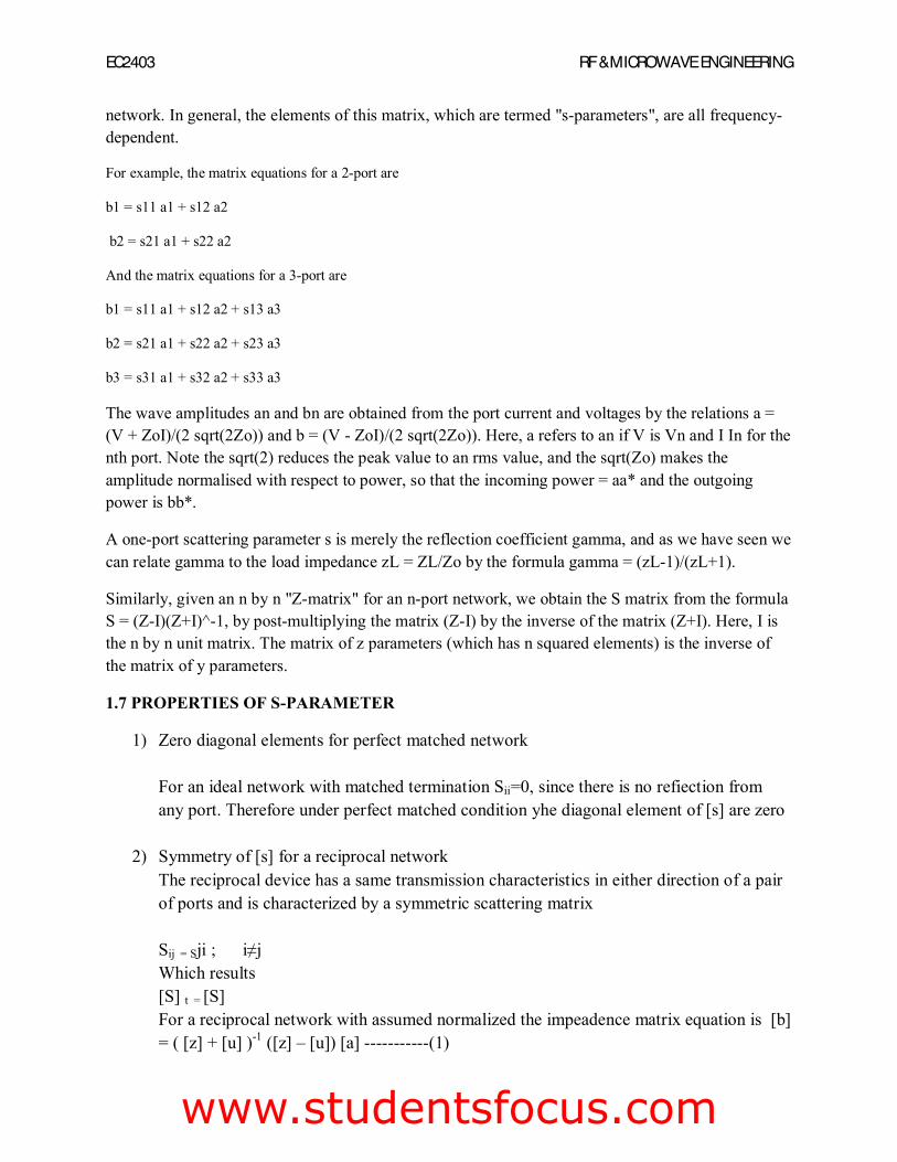
network. In general, the elements of this matrix, which are termed "s-parameters", are all frequency-dependent.
For example, the matrix equations for a 2-port are
b1 = s11 a1 + s12 a2
b2 = s21 a1 + s22 a2
And the matrix equations for a 3-port are
b1 = s11 a1 + s12 a2 + s13 a3
b2 = s21 a1 + s22 a2 + s23 a3
b3 = s31 a1 + s32 a2 + s33 a3
The wave amplitudes an and bn are obtained from the port current and voltages by the relations a = (V + ZoI)/(2 sqrt(2Zo)) and b = (V - ZoI)/(2 sqrt(2Zo)). Here, a refers to an if V is Vn and I In for the nth port. Note the sqrt(2) reduces the peak value to an rms value, and the sqrt(Zo) makes the amplitude normalised with respect to power, so that the incoming power = aa* and the outgoing power is bb*.
A one-port scattering parameter s is merely the reflection coefficient gamma, and as we have seen we can relate gamma to the load impedance zL = ZL/Zo by the formula gamma = (zL-1)/(zL+1).
Similarly, given an n by n "Z-matrix" for an n-port network, we obtain the S matrix from the formula S = (Z-I)(Z+I)^-1, by post-multiplying the matrix (Z-I) by the inverse of the matrix (Z+I). Here, I is the n by n unit matrix. The matrix of z parameters (which has n squared elements) is the inverse of the matrix of y parameters.
1.7 PROPERTIES OF S-PARAMETER
1) Zero diagonal elements for perfect matched network For an ideal network with matched termination Sii=0, since there is no refiection from any port. Therefore under perfect matched condition yhe diagonal element of [s] are zero
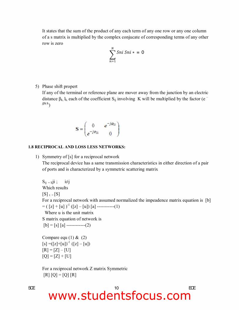
2) Symmetry of [s] for a reciprocal network The reciprocal device has a same transmission characteristics in either direction of a pair of ports and is characterized by a symmetric scattering matrix Sij = Sji ; i≠j Which results [S] t = [S] For a reciprocal network with assumed normalized the impeadence matrix equation is [b] = ( [z] + [u] )-1 ([z] – [u]) [a] -----------(1)
Fatima Michael College of Engineering & Technology
Fatima Michael College of Engineering & Technology
Fatima Michael College of Engineering & Technologywww.studentsfocus.com

Where u is the unit matrix S matrix equation of network is [b] = [s] [a] ------------(2) Compare equ (1) & (2) [s] =([z]+[u])-1 ([z] – [u]) [R] = [Z] – [U] [Q] = [Z] + [U] For a reciprocal network Z matrix Symmetric [R] [Q] = [Q] [R] [Q] -1[R][Q][Q]-1 = [Q]-1[Q][R][Q]-1
[Q] -1[R] = [R][Q]-1
[Q] -1[R] [ S ] = [R][Q]-1 ------------(3) TRANSPOSE OS [s] IS NOW GIVEN AS [S]t = [Z-u]t [ Z+U]t -1 Then [Z-u]t = [ Z-U] [Z+u]t
-1 = [ Z+U] [S] t = [z-u] [z+u]-1
[S] t = [R][Q]-1 -------------(4) When compare 3 & 4 [S] t = [S]
3) Unitary property of lossless network
For any loss less network the sum of product of each term of any one row or any one column of s matrix multiplied by its complex conjugate is unity
푆푛푖 푆푛푖 ∗ = 1
For a lossless N port devices the total power leaving N ports must be equal to total input to the ports
4) Zero property
Fatima Michael College of Engineering & Technology
Fatima Michael College of Engineering & Technology
Fatima Michael College of Engineering & Technologywww.studentsfocus.com
SCE 10 ECE
It states that the sum of the product of any each term of any one row or any one column of a s matrix is multiplied by the complex conjucate of corresponding terms of any other row is zero
푆푛푖 푆푛푖 ∗ = 0
5) Phase shift propert
If any of the terminal or reference plane are mover away from the junction by an electric distance βk, lk. each of the coefficient Sij involving K will be multiplied by the factor (e –
jβk/k)
1.8 RECIPROCAL AND LOSS LESS NETWORKS:
1) Symmetry of [s] for a reciprocal network The reciprocal device has a same transmission characteristics in either direction of a pair of ports and is characterized by a symmetric scattering matrix Sij = Sji ; i≠j Which results [S] t = [S] For a reciprocal network with assumed normalized the impeadence matrix equation is [b] = ( [z] + [u] )-1 ([z] – [u]) [a] -----------(1) Where u is the unit matrix S matrix equation of network is [b] = [s] [a] ------------(2) Compare equ (1) & (2) [s] =([z]+[u])-1 ([z] – [u]) [R] = [Z] – [U] [Q] = [Z] + [U] For a reciprocal network Z matrix Symmetric [R] [Q] = [Q] [R]
Fatima Michael College of Engineering & Technology
Fatima Michael College of Engineering & Technology
Fatima Michael College of Engineering & Technologywww.studentsfocus.com
[Q] -1[R][Q][Q]-1 = [Q]-1[Q][R][Q]-1
[Q] -1[R] = [R][Q]-1
[Q] -1[R] [ S ] = [R][Q]-1
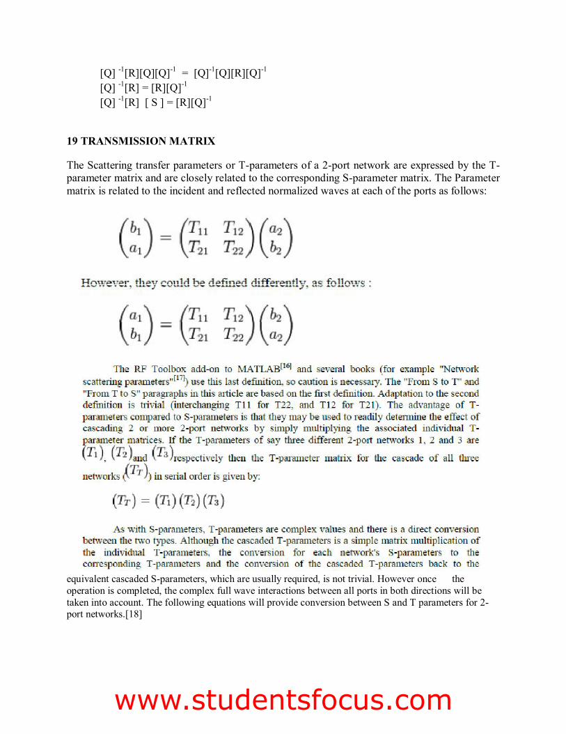
19 TRANSMISSION MATRIX
The Scattering transfer parameters or T-parameters of a 2-port network are expressed by the T-parameter matrix and are closely related to the corresponding S-parameter matrix. The Parameter matrix is related to the incident and reflected normalized waves at each of the ports as follows:
equivalent cascaded S-parameters, which are usually required, is not trivial. However once the operation is completed, the complex full wave interactions between all ports in both directions will be taken into account. The following equations will provide conversion between S and T parameters for 2-port networks.[18]
Fatima Michael College of Engineering & Technology
Fatima Michael College of Engineering & Technology
Fatima Michael College of Engineering & Technologywww.studentsfocus.com
1.10 INTODUCTION TO COMPONENT BASICS:
WIRE
CAPACITOR
INDUCTOR
RESISTOR
1.11 WIRE:
RF Cable Assembly is a quality manufacturer of standard and custom cable assemblies and electromechanical wiring harnesses for medical, computer, LAN, RF, automotive, monitoring and communications equipment. We can build custom cables to meet your requirements, whether standard or special. Complete product design, tooling design and fabrication, materials processing and selection, product manufacture, assembly, testing and packaging are available in our San Diego facility.
Fatima Michael College of Engineering & Technology
Fatima Michael College of Engineering & Technology
Fatima Michael College of Engineering & Technologywww.studentsfocus.com
All our assembly and soldering technicians have been trained to the requirements of IPC/EIA J-STD-001 and IPC/WHMA-A-620. By creating and using hand tools and assembly jigs designed for their tasks and using them in our documented production processes, we produce quality with repeatability.
1.12 RESISTOR:
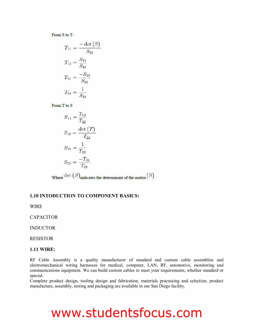
The H, Y, Z and ABCD parameters are difficult at microwave frequencies due to the following reasons. (i)Equipment is not readily available to measure total voltage and total current at the ports of the network. (ii) Short circuit and open circuit are difficult to achieve over a wide range of frequencies. (iii) Presence of active devices makes the circuit unstable for short or open circuit. Therefore microwave circuits are analyzed using scattering or S parameters which linearly relate the reflected wave amplitude with those of incident waves.
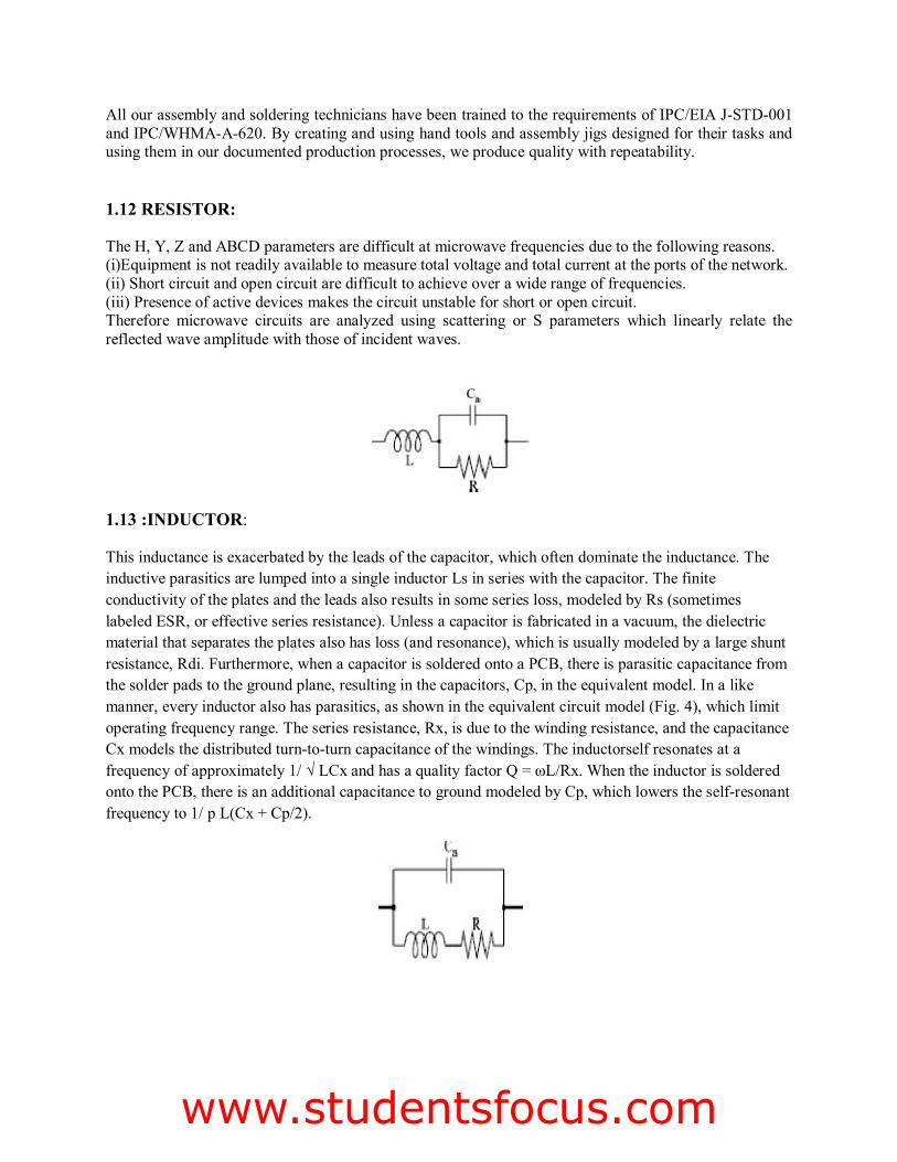
1.13 :INDUCTOR:
This inductance is exacerbated by the leads of the capacitor, which often dominate the inductance. The inductive parasitics are lumped into a single inductor Ls in series with the capacitor. The finite conductivity of the plates and the leads also results in some series loss, modeled by Rs (sometimes labeled ESR, or effective series resistance). Unless a capacitor is fabricated in a vacuum, the dielectric material that separates the plates also has loss (and resonance), which is usually modeled by a large shunt resistance, Rdi. Furthermore, when a capacitor is soldered onto a PCB, there is parasitic capacitance from the solder pads to the ground plane, resulting in the capacitors, Cp, in the equivalent model. In a like manner, every inductor also has parasitics, as shown in the equivalent circuit model (Fig. 4), which limit operating frequency range. The series resistance, Rx, is due to the winding resistance, and the capacitance Cx models the distributed turn-to-turn capacitance of the windings. The inductorself resonates at a frequency of approximately 1/ √ LCx and has a quality factor Q = ωL/Rx. When the inductor is soldered
onto the PCB, there is an additional capacitance to ground modeled by Cp, which lowers the self-resonant frequency to 1/ p L(Cx + Cp/2).
Fatima Michael College of Engineering & Technology
Fatima Michael College of Engineering & Technology
Fatima Michael College of Engineering & Technologywww.studentsfocus.com

1.14: CAPACITOR:
now you have probably simulated your circuits with ideal passive components (inductors, capacitors, resistors), but real circuit components are far from ideal. Consider, for instance, a capacitor, which has an equivalent circuit model shown in Fig. 2. The model has many parasitic components which only become relevant at high frequencies. A plot of the impedance of the capacitor, shown in Fig. 3, shows that in addition to the ideal behavior, the most notable difference is the self-resonance that occurs for any real capacitor. The selfresonance is inevitable for any real capacitor due to the fact that as AC currents flow through a capacitor, a magnetic field is also generated by the capacitor, which leads to inductance
Fatima Michael College of Engineering & Technology
Fatima Michael College of Engineering & Technology
Fatima Michael College of Engineering & Technologywww.studentsfocus.com
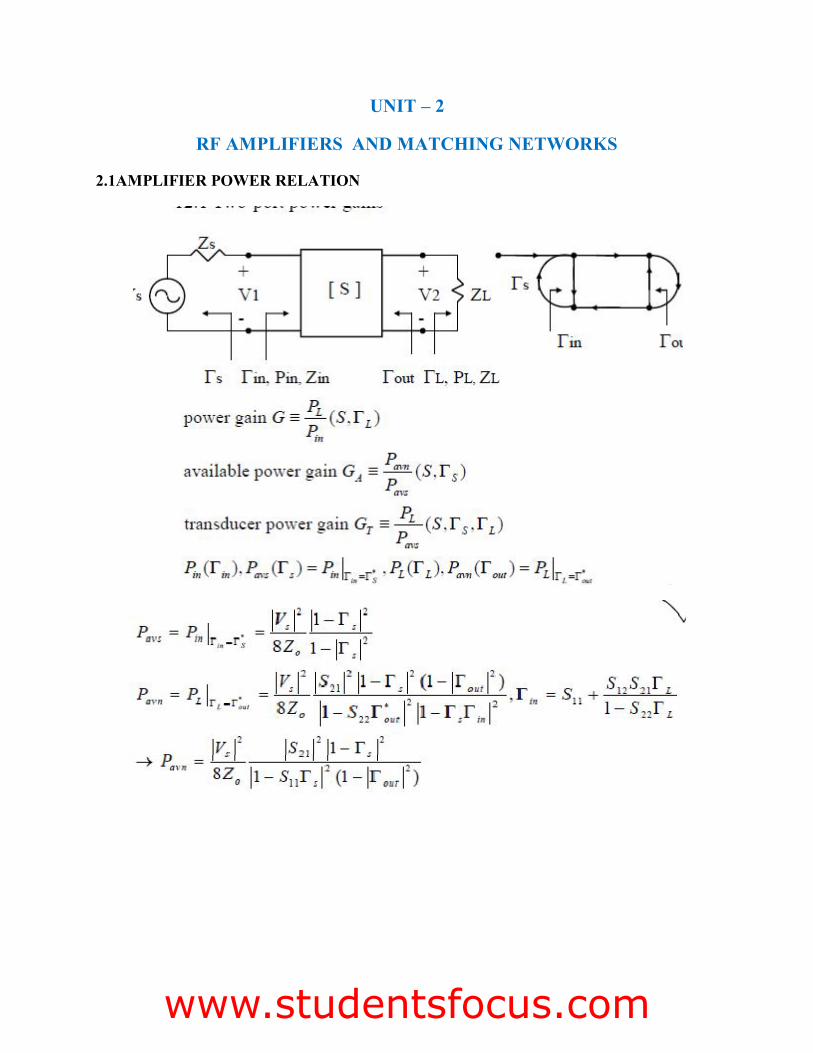
2.1AMPLIFIER POWER RELATION
UNIT – 2
RF AMPLIFIERS AND MATCHING NETWORKS
Fatima Michael College of Engineering & Technology
Fatima Michael College of Engineering & Technology
Fatima Michael College of Engineering & Technologywww.studentsfocus.com

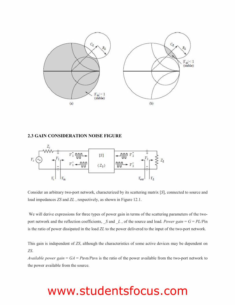
2.2 STABILITY CONSIDERATION AND FREQUENCY RESPONSE:
9 Unconditional stability: The network is unconditionally stable if[ Гin] <1 and [Гout]<1 for all
passive source and load impedances(i.e Гs<1 and ГL<1)
9 Conditional stability: The network is conditionally stable if |_in| < 1 and |_out| < 1 only for a
certain range of passive source and load impedances. This case is also referred to as potentially
unstable.
Stability Circles
9 Applying the above requirements for unconditional stability to (12.3) gives the following
conditions that must be satisfied by _S and _L if the amplifier is to be unconditionally
9 We can derive the equation for the output stability circle as follows. First use (12.19a) to express
the condition that |_in| = 1 as
or
Now define _ as the determinant of the scattering matrix:
Fatima Michael College of Engineering & Technology
Fatima Michael College of Engineering & Technology
Fatima Michael College of Engineering & Technologywww.studentsfocus.com

Then we can write the above result as
Now square both sides and simplify to obtain
Fatima Michael College of Engineering & Technology
Fatima Michael College of Engineering & Technology
Fatima Michael College of Engineering & Technologywww.studentsfocus.com
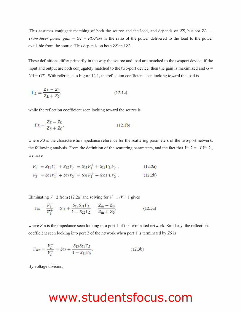
2.3 GAIN CONSIDERATION NOISE FIGURE
Consider an arbitrary two-port network, characterized by its scattering matrix [S], connected to source and
load impedances ZS and ZL , respectively, as shown in Figure 12.1.
We will derive expressions for three types of power gain in terms of the scattering parameters of the two-
port network and the reflection coefficients, _S and _L , of the source and load. Power gain = G = PL/Pin
is the ratio of power dissipated in the load ZL to the power delivered to the input of the two-port network.
This gain is independent of ZS, although the characteristics of some active devices may be dependent on
ZS.
Available power gain = GA = Pavn/Pavs is the ratio of the power available from the two-port network to
the power available from the source.
Fatima Michael College of Engineering & Technology
Fatima Michael College of Engineering & Technology
Fatima Michael College of Engineering & Technologywww.studentsfocus.com
This assumes conjugate matching of both the source and the load, and depends on ZS, but not ZL . _
Transducer power gain = GT = PL/Pavs is the ratio of the power delivered to the load to the power
available from the source. This depends on both ZS and ZL .
These definitions differ primarily in the way the source and load are matched to the twoport device; if the
input and output are both conjugately matched to the two-port device, then the gain is maximized and G =
GA = GT . With reference to Figure 12.1, the reflection coefficient seen looking toward the load is
while the reflection coefficient seen looking toward the source is
where Z0 is the characteristic impedance reference for the scattering parameters of the two-port network.
the following analysis. From the definition of the scattering parameters, and the fact that V+ 2 = _LV− 2 ,
we have
Eliminating V− 2 from (12.2a) and solving for V− 1 /V + 1 gives
where Zin is the impedance seen looking into port 1 of the terminated network. Similarly, the reflection
coefficient seen looking into port 2 of the network when port 1 is terminated by ZS is
By voltage division,
Fatima Michael College of Engineering & Technology
Fatima Michael College of Engineering & Technology
Fatima Michael College of Engineering & Technologywww.studentsfocus.com

Using
from (12.3a) and solving for V+
1 in terms of VS gives
If peak values are assumed for all voltages, the average power delivered to the network is
where (12.4) was used. The power delivered to the load is
Solving for V−
2 from (12.2b), substituting into (12.6), and using (12.4) gives
The power gain can then be expressed as
The power available from the source, Pavs, is the maximum power that can be delivered to the network.
This occurs when the input impedance of the terminated network is conjugately matched to the source
Fatima Michael College of Engineering & Technology
Fatima Michael College of Engineering & Technology
Fatima Michael College of Engineering & Technologywww.studentsfocus.com

impedance, as discussed in Section 2.6. Thus, from (12.5),
Similarly, the power available from the network, Pavn, is the maximum power that can be delivered to the
load. Thus, from (12.7),
In (12.10), _in must be evaluated for _L = _ out. From (12.3a), it can be shown that
which reduces (12.10) to
Observe that Pavs and Pavn have been expressed in terms of the source voltage, VS, which is independent
of the input or load impedances. There would be confusion if these quantities were expressed in terms of
V+ 1 since V+ 1 is different for each of the calculations of PL , Pavs, and Pavn. Using (12.11) and (12.9),
we obtain the available power gain as
From (12.7) and (12.9), the transducer power gain is
A special case of the transducer power gain occurs when both the input and output are matched for zero
reflection (in contrast to conjugate matching). Then _L = _S = 0, and (12.13) reduces to
Fatima Michael College of Engineering & Technology
Fatima Michael College of Engineering & Technology
Fatima Michael College of Engineering & Technologywww.studentsfocus.com
Another special case is the unilateral transducer power gain, GTU, where S12 = 0 (or is negligibly
small). This nonreciprocal characteristic is approximately true for many transistors devices. From (12.3a),
_in = S11 when S12 = 0, so (12.13) gives the unilateral transducer power gain as
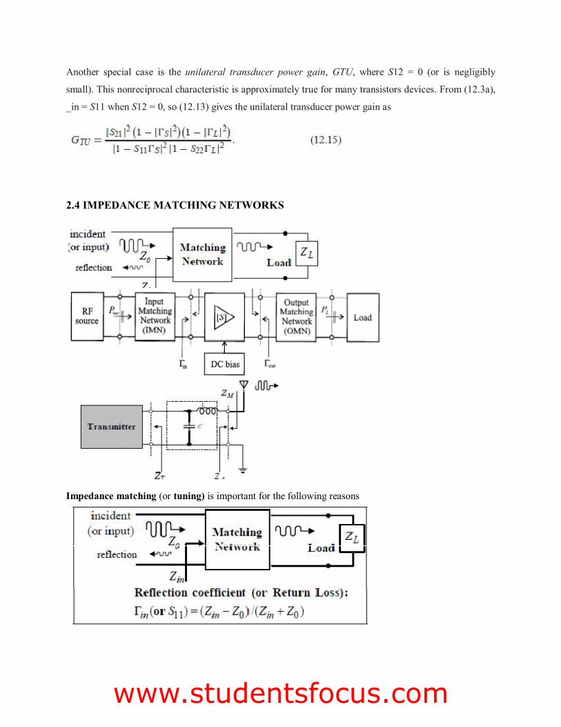
2.4 IMPEDANCE MATCHING NETWORKS
Impedance matching (or tuning) is important for the following reasons
Fatima Michael College of Engineering & Technology
Fatima Michael College of Engineering & Technology
Fatima Michael College of Engineering & Technologywww.studentsfocus.com
9 minimum power loss in the feed line & maximum power delivery
9 linearizing the frequency response of the circuit
9 improving the S/N ratio of the system for sensitive receiver components (lownoise amplifier,
etc.)
9 reducing amplitude & phase errors in a power distribution network (such as antenna array-
feed network)
Factors in the selection of matching networks
9 complexity -bandwidth requirement (such as broadband design) - adjustability
9 implementation (by using transmission line, chip R/L/C elements ..)
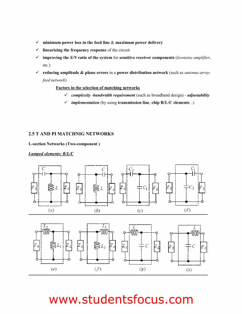
2.5 T AND PI MATCHNIG NETWORKS
L-section Networks (Two-component )
Lumped elements: R/L/C
Fatima Michael College of Engineering & Technology
Fatima Michael College of Engineering & Technology
Fatima Michael College of Engineering & Technologywww.studentsfocus.com
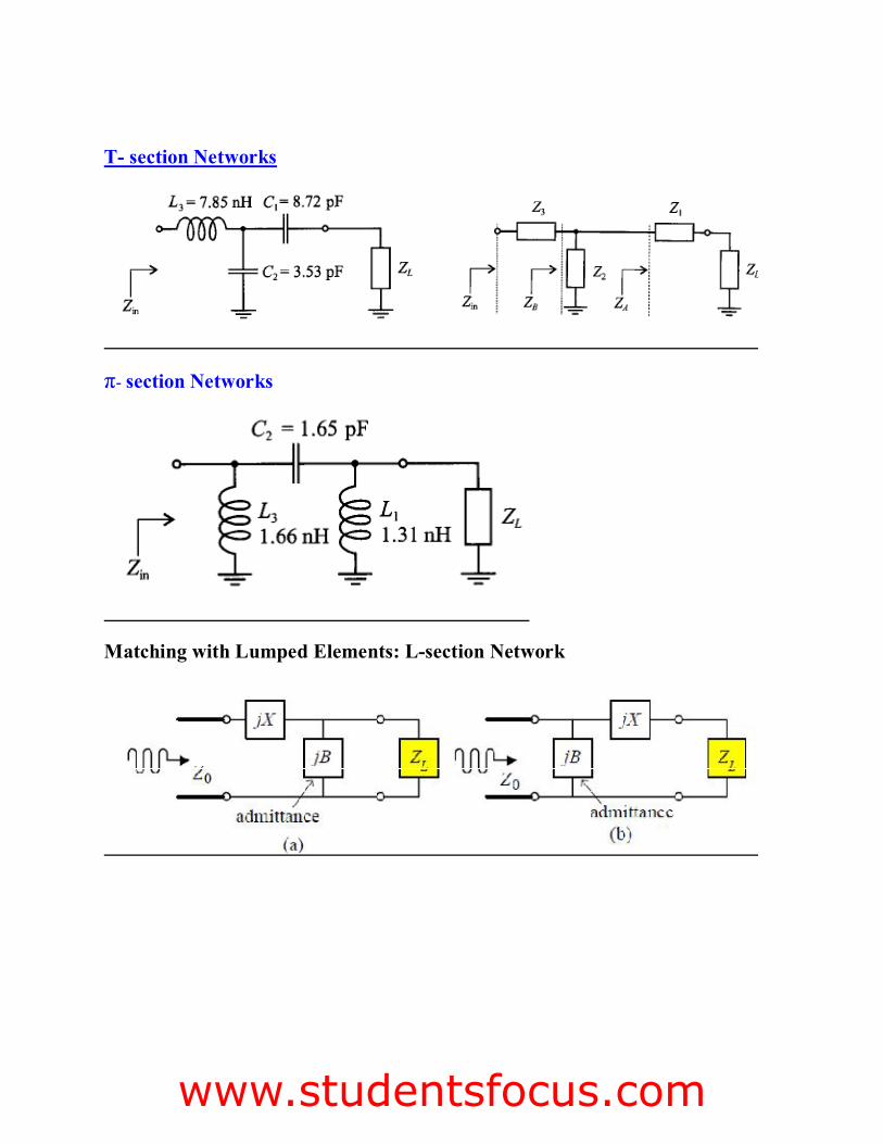
T- section Networks
π- section Networks
Matching with Lumped Elements: L-section Network
Fatima Michael College of Engineering & Technology
Fatima Michael College of Engineering & Technology
Fatima Michael College of Engineering & Technologywww.studentsfocus.com
Fatima Michael College of Engineering & Technology
Fatima Michael College of Engineering & Technology
Fatima Michael College of Engineering & Technologywww.studentsfocus.com
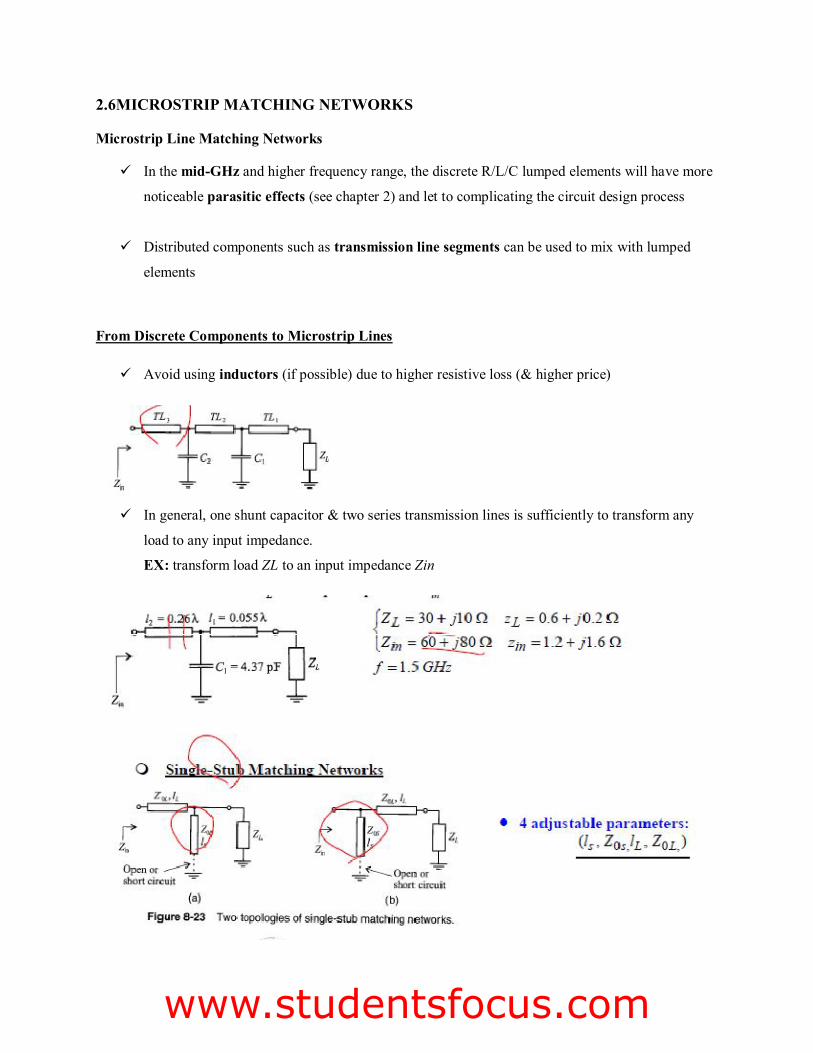
2.6MICROSTRIP MATCHING NETWORKS
Microstrip Line Matching Networks
9 In the mid-GHz and higher frequency range, the discrete R/L/C lumped elements will have more
noticeable parasitic effects (see chapter 2) and let to complicating the circuit design process
9 Distributed components such as transmission line segments can be used to mix with lumped
elements
From Discrete Components to Microstrip Lines
9 Avoid using inductors (if possible) due to higher resistive loss (& higher price)
9 In general, one shunt capacitor & two series transmission lines is sufficiently to transform any
load to any input impedance.
EX: transform load ZL to an input impedance Zin
Fatima Michael College of Engineering & Technology
Fatima Michael College of Engineering & Technology
Fatima Michael College of Engineering & Technologywww.studentsfocus.com

UNIT – 3
MICROWAVE PASSIVE COMPONENTS
3.1 :MICROWAVE FREQUENCY RANGE:
Microwaves are electromagnetic waves with wavelengths ranging from 1 mm to 1 m, or frequencies between 300 MHz and 300 GHz.
L band 1 to 2 GHz
S band 2 to 4 GHz
C band 4 to 8 GHz
X band 8 to 12 GHz
Ku band 12 to 18GH GHz
K band 18 to 26.5 GHz
Ka band 26.5 to 40 GHz
Q band 30 to 50 GHz
U band 40 to 60 GHz
V band 50 to 75 GHz
3.2:SIGNIFICANCE MICROWAVE FREQUENCY RANGE:
Wireless LAN protocols, such as Bluetooth and the IEEE 802.11 specifications, also use microwaves in the 2.4 GHz ISM band, although 802.11a uses ISM band and U-NII frequencies in the 5 GHz range. Licensed long-range (up to about 25 km) Wireless Internet Access services can be found in many countries (but not the USA) in the 3.5–4.0 GHz range. Metropolitan Area Networks: MAN protocols, such as WiMAX (Worldwide Interoperability for Microwave Access) based in the IEEE 802.16 specification. The IEEE 802.16 specification was designed to operate between 2 to 11 GHz. The commercial implementations are in the 2.3GHz, 2.5 GHz, 3.5 GHz and 5.8 GHz ranges.
Fatima Michael College of Engineering & Technology
Fatima Michael College of Engineering & Technology
Fatima Michael College of Engineering & Technologywww.studentsfocus.com

Wide Area Mobile Broadband Wireless Access: MBWA protocols based on standards specifications such as IEEE 802.20 or ATIS/ANSI HC-SDMA (e.g. iBurst) are designed to operate between 1.6 and 2.3 GHz to give mobility and in-building penetration characteristics similar to mobile phones but with vastly greater spectral efficiency. Cable TV and Internet access on coaxial cable as well as broadcast television use some of the lower microwave frequencies. Some mobile phone networks, like GSM, also use the lower microwave frequencies.
3.3 :APPLICATION OF MICROWAVE:
1.FM Brodcasting
2.CDMA mobile phone
3.GSM Mobile phone
4. Cable television relay
5.Geostationary fixed satellite service
6.Marine airborne radar
7.Remote sensing radar
3.4: SCATTERING MATRIX:
"Scattering" is an idea taken from billiards, or pool. One takes a cue ball and fires it up the table at a collection of other balls. After the impact, the energy and momentum in the cue ball is divided between all the balls involved in the impact. The cue ball "scatters" the stationary target balls and in turn is deflected or "scattered" by them. In a microwave circuit, the equivalent to the energy and momentum of the cue ball is the amplitude and phase of the incoming wave on a transmission line. (A rather loose analogy, this). This incoming wave is "scattered" by the circuit and its energy is partitioned between all the possible outgoing waves on all the other transmission lines connected to the circuit. The scattering parameters are fixed properties of the (linear) circuit which describe how the energy couples between each pair of ports or transmission lines connected to the circuit.
Formally, s-parameters can be defined for any collection of linear electronic components, whether or not the wave view of the power flow in the circuit is necessary. They are algebraically related to the impedance parameters (z-parameters), also to the admittance parameters (y-parameters) and to a notional characteristic impedance of the transmission lines.
Fatima Michael College of Engineering & Technology
Fatima Michael College of Engineering & Technology
Fatima Michael College of Engineering & Technologywww.studentsfocus.com
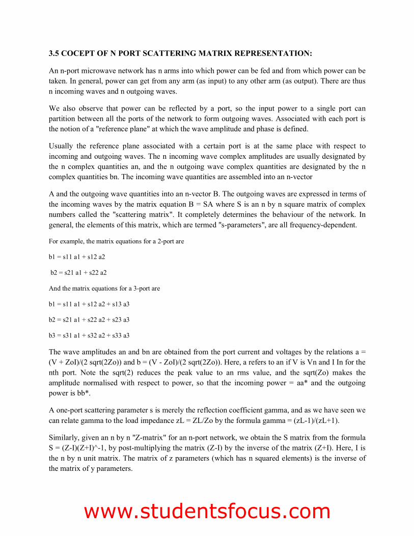
3.5 COCEPT OF N PORT SCATTERING MATRIX REPRESENTATION:
An n-port microwave network has n arms into which power can be fed and from which power can be taken. In general, power can get from any arm (as input) to any other arm (as output). There are thus n incoming waves and n outgoing waves.
We also observe that power can be reflected by a port, so the input power to a single port can partition between all the ports of the network to form outgoing waves. Associated with each port is the notion of a "reference plane" at which the wave amplitude and phase is defined.
Usually the reference plane associated with a certain port is at the same place with respect to incoming and outgoing waves. The n incoming wave complex amplitudes are usually designated by the n complex quantities an, and the n outgoing wave complex quantities are designated by the n complex quantities bn. The incoming wave quantities are assembled into an n-vector
A and the outgoing wave quantities into an n-vector B. The outgoing waves are expressed in terms of the incoming waves by the matrix equation B = SA where S is an n by n square matrix of complex numbers called the "scattering matrix". It completely determines the behaviour of the network. In general, the elements of this matrix, which are termed "s-parameters", are all frequency-dependent.
For example, the matrix equations for a 2-port are
b1 = s11 a1 + s12 a2
b2 = s21 a1 + s22 a2
And the matrix equations for a 3-port are
b1 = s11 a1 + s12 a2 + s13 a3
b2 = s21 a1 + s22 a2 + s23 a3
b3 = s31 a1 + s32 a2 + s33 a3
The wave amplitudes an and bn are obtained from the port current and voltages by the relations a = (V + ZoI)/(2 sqrt(2Zo)) and b = (V - ZoI)/(2 sqrt(2Zo)). Here, a refers to an if V is Vn and I In for the nth port. Note the sqrt(2) reduces the peak value to an rms value, and the sqrt(Zo) makes the amplitude normalised with respect to power, so that the incoming power = aa* and the outgoing power is bb*.
A one-port scattering parameter s is merely the reflection coefficient gamma, and as we have seen we can relate gamma to the load impedance zL = ZL/Zo by the formula gamma = (zL-1)/(zL+1).
Similarly, given an n by n "Z-matrix" for an n-port network, we obtain the S matrix from the formula S = (Z-I)(Z+I)^-1, by post-multiplying the matrix (Z-I) by the inverse of the matrix (Z+I). Here, I is the n by n unit matrix. The matrix of z parameters (which has n squared elements) is the inverse of the matrix of y parameters.
Fatima Michael College of Engineering & Technology
Fatima Michael College of Engineering & Technology
Fatima Michael College of Engineering & Technologywww.studentsfocus.com

3.6 PROPRTIES OF S MATRIX
1) Zero diagonal elements for perfect matched network For an ideal network with matched termination Sii=0, since there is no refiection from any port. Therefore under perfect matched condition yhe diagonal element of [s] are zero
2) Symmetry of [s] for a reciprocal network The reciprocal device has a same transmission characteristics in either direction of a pair of ports and is characterized by a symmetric scattering matrix Sij = Sji ; i≠j Which results [S] t = [S] For a reciprocal network with assumed normalized the impeadence matrix equation is [b] = ( [z] + [u] )-1 ([z] – [u]) [a] -----------(1) Where u is the unit matrix S matrix equation of network is [b] = [s] [a] ------------(2) Compare equ (1) & (2) [s] =([z]+[u])-1 ([z] – [u]) [R] = [Z] – [U] [Q] = [Z] + [U] For a reciprocal network Z matrix Symmetric [R] [Q] = [Q] [R] [Q] -1[R][Q][Q]-1 = [Q]-1[Q][R][Q]-1
[Q] -1[R] = [R][Q]-1
[Q] -1[R] [ S ] = [R][Q]-1 ------------(3) TRANSPOSE OS [s] IS NOW GIVEN AS [S]t = [Z-u]t [ Z+U]t -1 Then [Z-u]t = [ Z-U] [Z+u]t
-1 = [ Z+U] [S] t = [z-u] [z+u]-1
[S] t = [R][Q]-1 -------------(4)
Fatima Michael College of Engineering & Technology
Fatima Michael College of Engineering & Technology
Fatima Michael College of Engineering & Technologywww.studentsfocus.com

When compare 3 & 4 [S] t = [S]
3) Unitary property of lossless network
For any loss less network the sum of product of each term of any one row or any one column of s matrix multiplied by its complex conjugate is unity
푆푛푖 푆푛푖 ∗ = 1
For a lossless N port devices the total power leaving N ports must be equal to total input to the ports
4) Zero property It states that the sum of the product of any each term of any one row or any one column of a s matrix is multiplied by the complex conjucate of corresponding terms of any other row is zero
푆푛푖 푆푛푖 ∗ = 0
5) Phase shift propert
If any of the terminal or reference plane are mover away from the junction by an electric distance βk, lk. each of the coefficient Sij involving K will be multiplied by the factor (e –
jβk/k)
Fatima Michael College of Engineering & Technology
Fatima Michael College of Engineering & Technology
Fatima Michael College of Engineering & Technologywww.studentsfocus.com

3.7 S MATRIX FORMULATION OF TWO PORT JUNCTION
In the case of a microwave network having two ports only, an input and an output, the s-matrix has four s-parameters, designated s11 s12 s21 s22
These four complex quantites actually contain eight separate numbers; the real and imaginary parts, or the modulus and the phase angle, of each of the four complex scattering parameters. Let us consider the physical meaning of these s-parameters. If the output port 2 is terminated, that is, the transmission line is connected to a matched load impedance giving rise to no reflections, then there is no input wave on port 2.
The input wave on port 1 (a1) gives rise to a reflected wave at port 1 (s11a1) and a transmitted wave at port 2 which is absorbed in the termination on 2.
The transmitted wave size is (s21a1). If the network has no loss and no gain, the output power must equal the input power and so in this case |s11|̂ 2 + |s21|̂ 2 must equal unity. We see therefore that the sizes of S11 and S21 determine how the input power splits between the possible output paths.
3.8 MICROWAVE JUNCTIONS:
E PLANE TEE
H PLANE TEE
MAGIC TEE OR HYPRID TEE
3.9 : TEE JUNCTIONS:
Tee junctions. In microwave circuits a waveguide or coaxial-line junction with three
independent ports is commonly referred to as a tee junction.
From the S parameter theory of a microwave junction it is evident that a tee junction should be
characterized by a matrix of third order containing nine elements, six of which should be
independent.
The characteristics of a three-port junction can be explained by three theorems of the tee
junction. These theorems are derived from the equivalent- circuit representation of the tee
junction. Their statements follow
Fatima Michael College of Engineering & Technology
Fatima Michael College of Engineering & Technology
Fatima Michael College of Engineering & Technologywww.studentsfocus.com

1. A short circuit may always be placed in one of the arms of a three-port junction in such a way
that no power can be transferred through the other two arms.
2. If the junction is symmetric about one of its arms, a short circuit can always be placed in that
arm so that no reflections occur in power transmission between the other two arms. (That is, the
arms present matched impedances.)
3. It is impossible for a general three-port junction of arbitrary symmetry to present matched
impedances at all three arms.
H-plane tee (shunt tee). An H -plane tee is a waveguide tee in which the axis of its side arm is
"shunting" the E field or parallel to the H field of the main guide as shown in Fig.
It can be seen that if two input waves are fed into port 1 and port 2 of the collinear arm, the
output wave at port 3 will be in phase and additive. On the other hand, if the input is fed into port
3, the wave will split equally into port 1 and port 2 in phase and in the same magnitude.
Therefore the S matrix of the H -plane tee is similar to Eqs.
S13 = S23
[S] = 푆11 푆12 푆13푆21 푆22 푆23푆31 푆32 푆33
S13 = S 23 S33 = 0 S11 = S22 S13 = 1/√2
Fatima Michael College of Engineering & Technology
Fatima Michael College of Engineering & Technology
Fatima Michael College of Engineering & Technologywww.studentsfocus.com

S11 = 1/2
[S] = 1/ 2 −1/ 2 1/ √2−1/ 2 1/ 2 1/ √21/ √2 1/ √2 0
E -plane tee {series tee). An E -plane tee is a waveguide tee in which the axis of its side arm is parallel to
theE field of the main guide
If the collinear arms are symmetric about the side arm, there are two different transmission characteristics
It can be seen from Fig. 4-4-4 that if the Eplane tee is perfectly matched with the aid of screw tuners or
inductive or capacitive windows at the junction, the diagonal components of the scattering matrix, S1~,
Szz, and S33, are zero because there will be no reflection.
When the waves are fed into the side arm (port 3), the waves appearing at port 1 and port 2 of the
collinear arm will be in opposite phase and in the same magnitude. Therefore It should be noted that Eq.
does not mean that SI3 is always positive and S23
Fatima Michael College of Engineering & Technology
Fatima Michael College of Engineering & Technology
Fatima Michael College of Engineering & Technologywww.studentsfocus.com

is always negative. The negative sign merely means that Sl3 and S23 have opposite signs. For a matched
junction, the S matrix is given by
From the symmetry property of S matrix, the symmetric terms in Eq. ( 4-4-I3) are equal and they are
From the zero property of S matrix, the sum of the products of each term of any column (or row)
multiplied by the complex conjugate of the corresponding terms of any other column (or row) is zero and
it is
This means that either Sl3 or St3, or both, should be zero. However, from the unity property of S matrix,
the sum of the products of each term of any one row (or column) multiplied by its complex conjugate is
unity; that is,
Substitution of Eq. ( 4-4-I4) in ( 4-4-I7) results in
zero and thus Eq. ( 4-4-19) is false. In a similar fashion, if S23 = 0, then S 13 becomes zero and therefore
Eq. (4-4-20) is not true.
Fatima Michael College of Engineering & Technology
Fatima Michael College of Engineering & Technology
Fatima Michael College of Engineering & Technologywww.studentsfocus.com

This inconsistency proves the statement that the tee junction cannot be matched to the three arms. In other
words, the diagonal elements of the S matrix of a tee junction are not all zeros.
In general, when an £-plane tee is constructed of an empty waveguide, it is poorly matched at the tee
junction. Hence SiJ * 0 if i = j.
However, since the collinear arm is usually symmetric about the side arm, I S13l = I S23l and S11 = S22.
Then the S matrix can be simplified to
3.10 MAGIC TEE:
A magic tee is a combination of the E -plane tee and H -plane tee (refer to Fig. 4-4-7). The
magic tee has several characteristics:
1. If two waves of equal magnitude and the same phase are fed into port 1 and port 2, the output
will be zero at port 3 and additive at port 4.
2. If a wave is fed into port 4 (the Harm), it will be divided equally between port 1 and port 2 of
the collinear arms and will not appear at port 3 (the E arm).
3. If a wave is fed into port 3 (the E arm), it will produce an output of equal magnitude
Fatima Michael College of Engineering & Technology
Fatima Michael College of Engineering & Technology
Fatima Michael College of Engineering & Technologywww.studentsfocus.com

and opposite phase at port 1 and port 2. The output at port 4 is zero. That is, S43 = S34 = 0.
4. If a wave is fed into one of the collinear arms at port 1 or port 2, it will not appear in the other
collinear arm at port 2 or port 1 because the E arm causes a phase delay while the Harm causes a
phase advance. That is, S,z = Sz1 = 0.
Therefore the S matrix of a magic tee can be expressed as
The magic tee is commonly used for mixing, duplexing, and impedance measurements. Suppose,
for example, there are two identical radar transmitters in equipment stock.
A particular application requires twice more input power to an antenna than either transmitter
can deliver. A magic tee may be used to couple the two transmitters to the antenna in such a way
that the transmitters do not load each other.
The two transmitters should be connected to ports 3 and 4, respectively, as shown in Fig. 4-4-8.
Transmitter 1, connected to port 3, causes a wave to emanate from port 1 and another to emanate
from port 2; these waves are equal in magnitude but opposite in phase.
Similarly, transmitter 2, connected to port 4, gives rise to a wave at port 1 and another at port 2,
both equal in magnitude and in phase.
At port 1 the two opposite waves cancel each other. At port 2 the two in-phase waves add
together; so double output power at port 2 is obtained for the antenna as shown in Fig.
4-4-8.
Fatima Michael College of Engineering & Technology
Fatima Michael College of Engineering & Technology
Fatima Michael College of Engineering & Technologywww.studentsfocus.com
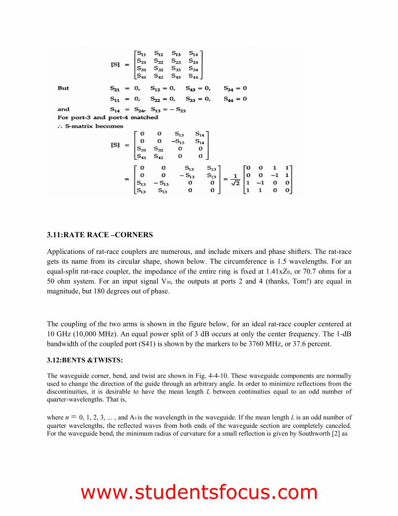
3.11:RATE RACE –CORNERS
Applications of rat-race couplers are numerous, and include mixers and phase shifters. The rat-race gets its name from its circular shape, shown below. The circumference is 1.5 wavelengths. For an equal-split rat-race coupler, the impedance of the entire ring is fixed at 1.41xZ0, or 70.7 ohms for a 50 ohm system. For an input signal Vin, the outputs at ports 2 and 4 (thanks, Tom!) are equal in magnitude, but 180 degrees out of phase.
The coupling of the two arms is shown in the figure below, for an ideal rat-race coupler centered at 10 GHz (10,000 MHz). An equal power split of 3 dB occurs at only the center frequency. The 1-dB bandwidth of the coupled port (S41) is shown by the markers to be 3760 MHz, or 37.6 percent.
3.12:BENTS &TWISTS:
The waveguide corner, bend, and twist are shown in Fig. 4-4-10. These waveguide components are normally used to change the direction of the guide through an arbitrary angle. In order to minimize reflections from the discontinuities, it is desirable to have the mean length L between continuities equal to an odd number of quarter-wavelengths. That is, where n = 0, 1, 2, 3, ... , and A8 is the wavelength in the waveguide. If the mean length L is an odd number of quarter wavelengths, the reflected waves from both ends of the waveguide section are completely canceled. For the waveguide bend, the minimum radius of curvature for a small reflection is given by Southworth [2] as
Fatima Michael College of Engineering & Technology
Fatima Michael College of Engineering & Technology
Fatima Michael College of Engineering & Technologywww.studentsfocus.com
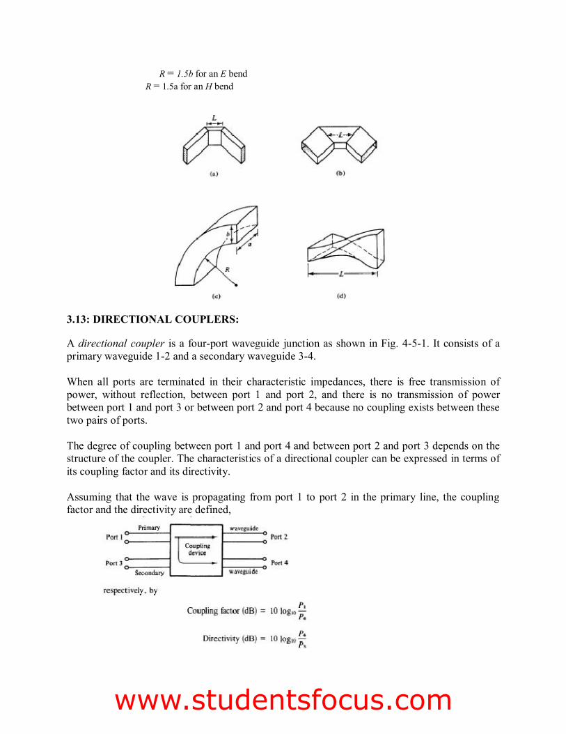
R = 1.5b for an E bend R = 1.5a for an H bend
3.13: DIRECTIONAL COUPLERS:
A directional coupler is a four-port waveguide junction as shown in Fig. 4-5-1. It consists of a primary waveguide 1-2 and a secondary waveguide 3-4. When all ports are terminated in their characteristic impedances, there is free transmission of power, without reflection, between port 1 and port 2, and there is no transmission of power between port 1 and port 3 or between port 2 and port 4 because no coupling exists between these two pairs of ports. The degree of coupling between port 1 and port 4 and between port 2 and port 3 depends on the structure of the coupler. The characteristics of a directional coupler can be expressed in terms of its coupling factor and its directivity. Assuming that the wave is propagating from port 1 to port 2 in the primary line, the coupling factor and the directivity are defined,
Fatima Michael College of Engineering & Technology
Fatima Michael College of Engineering & Technology
Fatima Michael College of Engineering & Technologywww.studentsfocus.com
where P, = power input to port 1 P3 = power output from port 3
P4 = power output from port 4
It should be noted that port 2, port 3, and port 4 are terminated in their characteristic impedances. The coupling factor is a measure of the ratio of power levels in the primary and secondary lines. Hence if the coupling factor is known, a fraction of power measured at port 4 may be used to determine the power input at port
1. This significance is desirable for microwave power measurements because no disturbance, which may be caused by the power measurements, occurs in the primary line.
2. The directivity is a measure of how well the forward traveling wave in the primary waveguide couples only to a specific port of the secondary waveguide. An ideal directional coupler should have infinite directivity. In other words, the power at port 3 must be zero because port 2 and port 4 are perfectly matched.
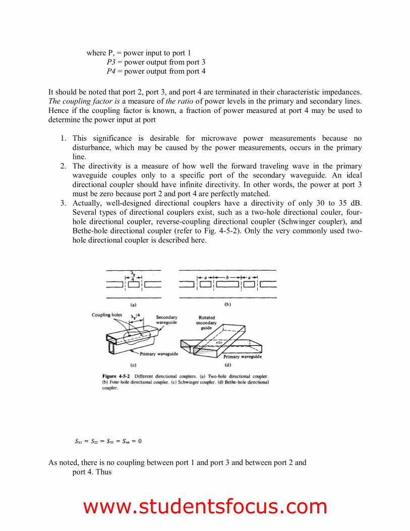
3. Actually, well-designed directional couplers have a directivity of only 30 to 35 dB. Several types of directional couplers exist, such as a two-hole directional couler, four-hole directional coupler, reverse-coupling directional coupler (Schwinger coupler), and Bethe-hole directional coupler (refer to Fig. 4-5-2). Only the very commonly used two-hole directional coupler is described here.
As noted, there is no coupling between port 1 and port 3 and between port 2 and port 4. Thus
Fatima Michael College of Engineering & Technology
Fatima Michael College of Engineering & Technology
Fatima Michael College of Engineering & Technologywww.studentsfocus.com

Consequently, the S matrix of a directional coupler becomes
Equation (4-5-6) can be further reduced by means of the zero property of the S matrix, so we have
Also from the unity property of the S matrix, we can write
Equations (4-5-7) and (4-5-8) can also be written
where q is positive and real. Then from Eq. (4-5-9)
The S matrix of a directional coupler is reduced to
Fatima Michael College of Engineering & Technology
Fatima Michael College of Engineering & Technology
Fatima Michael College of Engineering & Technologywww.studentsfocus.com
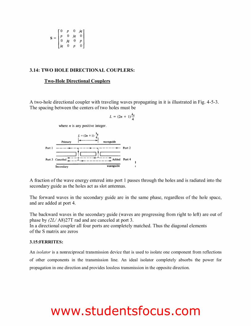
3.14: TWO HOLE DIRECTIONAL COUPLERS:
Two-Hole Directional Couplers
A two-hole directional coupler with traveling waves propagating in it is illustrated in Fig. 4-5-3. The spacing between the centers of two holes must be
A fraction of the wave energy entered into port 1 passes through the holes and is radiated into the secondary guide as the holes act as slot antennas. The forward waves in the secondary guide are in the same phase, regardless of the hole space, and are added at port 4. The backward waves in the secondary guide (waves are progressing from right to left) are out of phase by (2L/ A8)27T rad and are canceled at port 3. In a directional coupler all four ports are completely matched. Thus the diagonal elements of the S matrix are zeros
3.15:FERRITES:
An isolator is a nonreciprocal transmission device that is used to isolate one component from reflections
of other components in the transmission line. An ideal isolator completely absorbs the power for
propagation in one direction and provides lossless transmission in the opposite direction.
Fatima Michael College of Engineering & Technology
Fatima Michael College of Engineering & Technology
Fatima Michael College of Engineering & Technologywww.studentsfocus.com

Thus the isolator is usually called uniline. Isolators are generally used to improve the frequency stability
of microwave generators, such as klystrons and magnetrons, in which the reflection from the load affects
the generating frequency.
In such cases, the isolator placed between the generator and load prevents the reflected power from the
unmatched load from returning to the generator. As a result, the isolator maintains the frequency stability
of the generator. Isolators can be constructed in many ways.
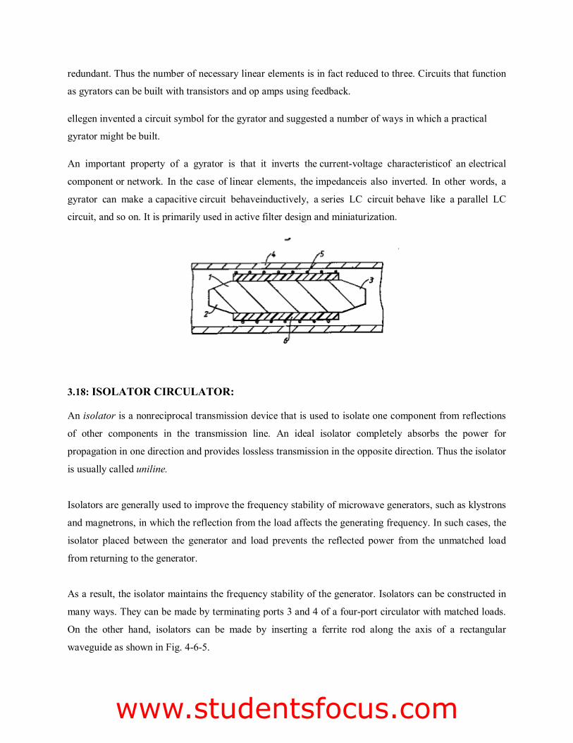
They can be made by terminating ports 3 and 4 of a four-port circulator with matched loads. On the other
hand, isolators can be made by inserting a ferrite rod along the axis of a rectangular waveguide as shown
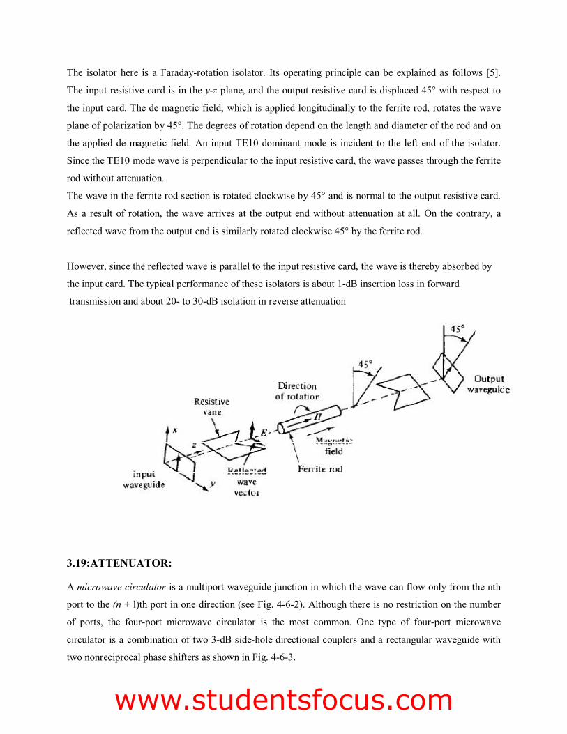
in Fig. 4-6-5. The isolator here is a Faraday-rotation isolator. Its operating principle can be explained as
follows [5]. The input resistive card is in the y-z plane, and the output resistive card is displaced 45° with
respect to the input card.
The de magnetic field, which is applied longitudinally to the ferrite rod, rotates the wave plane of
polarization by 45°. The degrees of rotation depend on the length and diameter of the rod and on the
applied de magnetic field. An input TE10 dominant mode is incident to the left end of the isolator. Since
the TE10 mode wave is perpendicular to the input resistive card, the wave passes through the ferrite rod
without attenuation.
The wave in the ferrite rod section is rotated clockwise by 45° and is normal to the output resistive card.
As a result of rotation, the wave arrives at the output
3.16:TERMINATION:
A microwave circulator is a multiport waveguide junction in which the wave can flow only from the nth
port to the (n + l)th port in one direction
Although there is no restriction on the number of ports, the four-port microwave circulator is the most
common. One type of four-port microwave circulator is a combination of two 3-dB side-hole directional
couplers and a rectangular waveguide with two nonreciprocal phase shifters as shown in Fig
Fatima Michael College of Engineering & Technology
Fatima Michael College of Engineering & Technology
Fatima Michael College of Engineering & Technologywww.studentsfocus.com
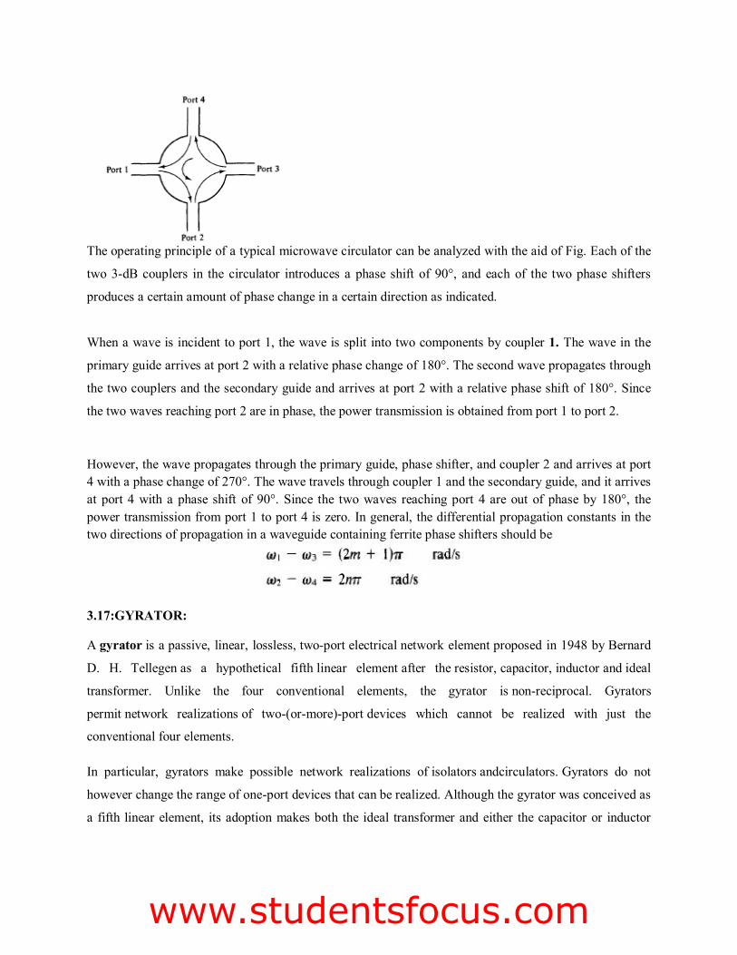
The operating principle of a typical microwave circulator can be analyzed with the aid of Fig. Each of the
two 3-dB couplers in the circulator introduces a phase shift of 90°, and each of the two phase shifters
produces a certain amount of phase change in a certain direction as indicated.
When a wave is incident to port 1, the wave is split into two components by coupler 1. The wave in the
primary guide arrives at port 2 with a relative phase change of 180°. The second wave propagates through
the two couplers and the secondary guide and arrives at port 2 with a relative phase shift of 180°. Since
the two waves reaching port 2 are in phase, the power transmission is obtained from port 1 to port 2.
However, the wave propagates through the primary guide, phase shifter, and coupler 2 and arrives at port 4 with a phase change of 270°. The wave travels through coupler 1 and the secondary guide, and it arrives at port 4 with a phase shift of 90°. Since the two waves reaching port 4 are out of phase by 180°, the power transmission from port 1 to port 4 is zero. In general, the differential propagation constants in the two directions of propagation in a waveguide containing ferrite phase shifters should be
3.17:GYRATOR:
A gyrator is a passive, linear, lossless, two-port electrical network element proposed in 1948 by Bernard
D. H. Tellegen as a hypothetical fifth linear element after the resistor, capacitor, inductor and ideal
transformer. Unlike the four conventional elements, the gyrator is non-reciprocal. Gyrators
permit network realizations of two-(or-more)-port devices which cannot be realized with just the
conventional four elements.
In particular, gyrators make possible network realizations of isolators andcirculators. Gyrators do not
however change the range of one-port devices that can be realized. Although the gyrator was conceived as
a fifth linear element, its adoption makes both the ideal transformer and either the capacitor or inductor
Fatima Michael College of Engineering & Technology
Fatima Michael College of Engineering & Technology
Fatima Michael College of Engineering & Technologywww.studentsfocus.com
redundant. Thus the number of necessary linear elements is in fact reduced to three. Circuits that function
as gyrators can be built with transistors and op amps using feedback.
ellegen invented a circuit symbol for the gyrator and suggested a number of ways in which a practical
gyrator might be built.
An important property of a gyrator is that it inverts the current-voltage characteristicof an electrical
component or network. In the case of linear elements, the impedanceis also inverted. In other words, a
gyrator can make a capacitive circuit behaveinductively, a series LC circuit behave like a parallel LC
circuit, and so on. It is primarily used in active filter design and miniaturization.
3.18: ISOLATOR CIRCULATOR:
An isolator is a nonreciprocal transmission device that is used to isolate one component from reflections
of other components in the transmission line. An ideal isolator completely absorbs the power for
propagation in one direction and provides lossless transmission in the opposite direction. Thus the isolator
is usually called uniline.
Isolators are generally used to improve the frequency stability of microwave generators, such as klystrons
and magnetrons, in which the reflection from the load affects the generating frequency. In such cases, the
isolator placed between the generator and load prevents the reflected power from the unmatched load
from returning to the generator.
As a result, the isolator maintains the frequency stability of the generator. Isolators can be constructed in
many ways. They can be made by terminating ports 3 and 4 of a four-port circulator with matched loads.
On the other hand, isolators can be made by inserting a ferrite rod along the axis of a rectangular
waveguide as shown in Fig. 4-6-5.
Fatima Michael College of Engineering & Technology
Fatima Michael College of Engineering & Technology
Fatima Michael College of Engineering & Technologywww.studentsfocus.com
The isolator here is a Faraday-rotation isolator. Its operating principle can be explained as follows [5].
The input resistive card is in the y-z plane, and the output resistive card is displaced 45° with respect to
the input card. The de magnetic field, which is applied longitudinally to the ferrite rod, rotates the wave
plane of polarization by 45°. The degrees of rotation depend on the length and diameter of the rod and on
the applied de magnetic field. An input TE10 dominant mode is incident to the left end of the isolator.
Since the TE10 mode wave is perpendicular to the input resistive card, the wave passes through the ferrite
rod without attenuation.
The wave in the ferrite rod section is rotated clockwise by 45° and is normal to the output resistive card.
As a result of rotation, the wave arrives at the output end without attenuation at all. On the contrary, a
reflected wave from the output end is similarly rotated clockwise 45° by the ferrite rod.
However, since the reflected wave is parallel to the input resistive card, the wave is thereby absorbed by
the input card. The typical performance of these isolators is about 1-dB insertion loss in forward
transmission and about 20- to 30-dB isolation in reverse attenuation
3.19:ATTENUATOR:
A microwave circulator is a multiport waveguide junction in which the wave can flow only from the nth
port to the (n + l)th port in one direction (see Fig. 4-6-2). Although there is no restriction on the number
of ports, the four-port microwave circulator is the most common. One type of four-port microwave
circulator is a combination of two 3-dB side-hole directional couplers and a rectangular waveguide with
two nonreciprocal phase shifters as shown in Fig. 4-6-3.
Fatima Michael College of Engineering & Technology
Fatima Michael College of Engineering & Technology
Fatima Michael College of Engineering & Technologywww.studentsfocus.com
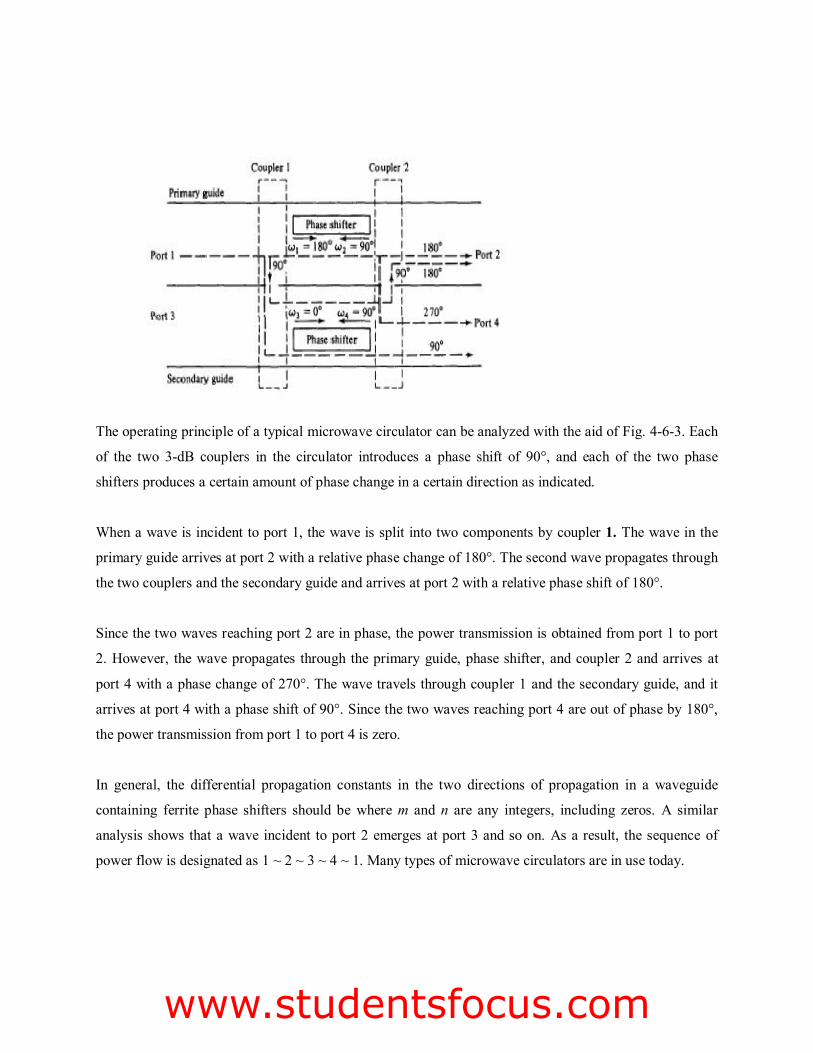
The operating principle of a typical microwave circulator can be analyzed with the aid of Fig. 4-6-3. Each
of the two 3-dB couplers in the circulator introduces a phase shift of 90°, and each of the two phase
shifters produces a certain amount of phase change in a certain direction as indicated.
When a wave is incident to port 1, the wave is split into two components by coupler 1. The wave in the
primary guide arrives at port 2 with a relative phase change of 180°. The second wave propagates through
the two couplers and the secondary guide and arrives at port 2 with a relative phase shift of 180°.
Since the two waves reaching port 2 are in phase, the power transmission is obtained from port 1 to port
2. However, the wave propagates through the primary guide, phase shifter, and coupler 2 and arrives at
port 4 with a phase change of 270°. The wave travels through coupler 1 and the secondary guide, and it
arrives at port 4 with a phase shift of 90°. Since the two waves reaching port 4 are out of phase by 180°,
the power transmission from port 1 to port 4 is zero.
In general, the differential propagation constants in the two directions of propagation in a waveguide
containing ferrite phase shifters should be where m and n are any integers, including zeros. A similar
analysis shows that a wave incident to port 2 emerges at port 3 and so on. As a result, the sequence of
power flow is designated as 1 ~ 2 ~ 3 ~ 4 ~ 1. Many types of microwave circulators are in use today.
Fatima Michael College of Engineering & Technology
Fatima Michael College of Engineering & Technology
Fatima Michael College of Engineering & Technologywww.studentsfocus.com
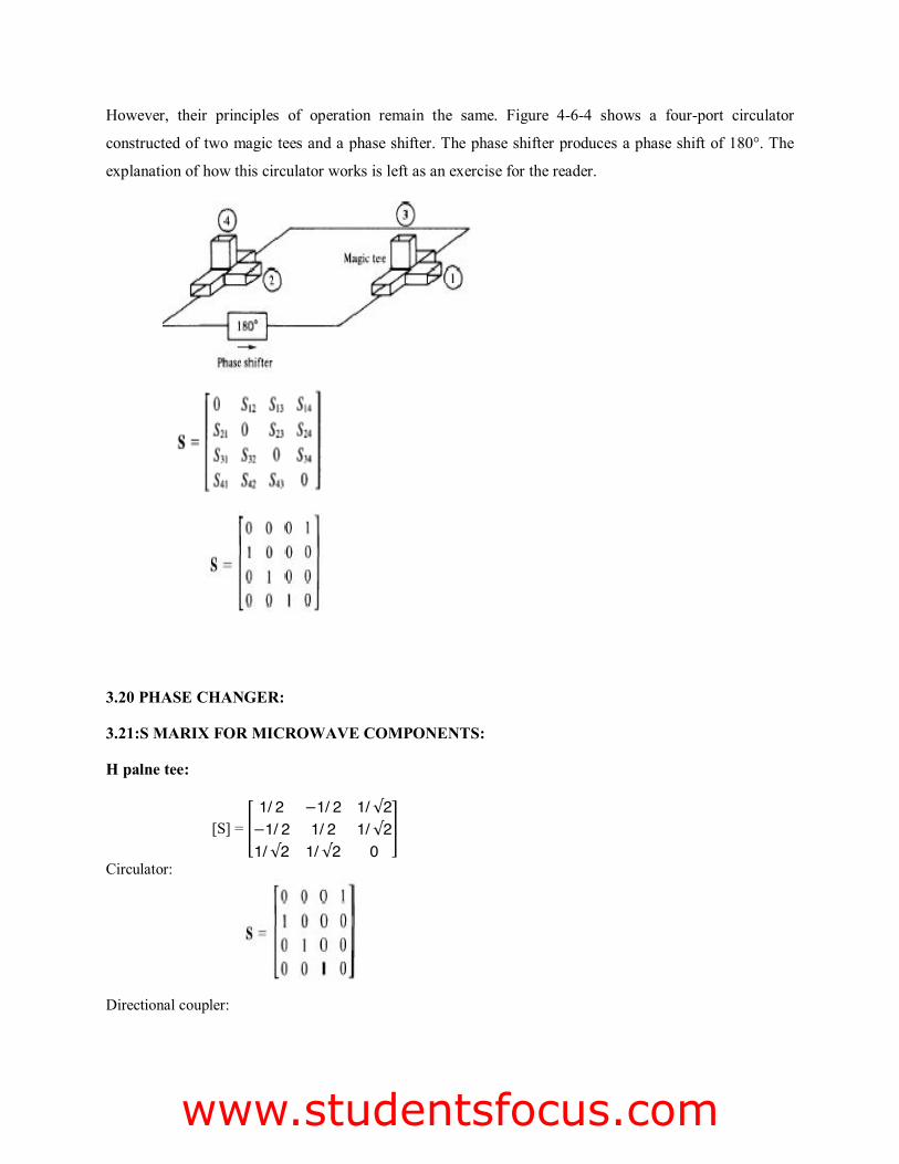
However, their principles of operation remain the same. Figure 4-6-4 shows a four-port circulator
constructed of two magic tees and a phase shifter. The phase shifter produces a phase shift of 180°. The
explanation of how this circulator works is left as an exercise for the reader.
3.20 PHASE CHANGER:
3.21:S MARIX FOR MICROWAVE COMPONENTS:
H palne tee:
[S] = 1/ 2 −1/ 2 1/ √2−1/ 2 1/ 2 1/ √21/ √2 1/ √2 0
Circulator:
Directional coupler:
Fatima Michael College of Engineering & Technology
Fatima Michael College of Engineering & Technology
Fatima Michael College of Engineering & Technologywww.studentsfocus.com
E palne Tee
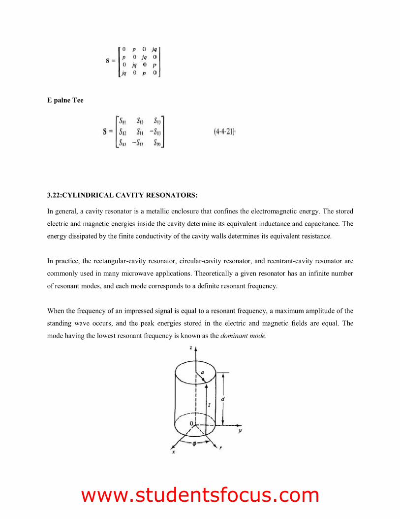
3.22:CYLINDRICAL CAVITY RESONATORS:
In general, a cavity resonator is a metallic enclosure that confines the electromagnetic energy. The stored
electric and magnetic energies inside the cavity determine its equivalent inductance and capacitance. The
energy dissipated by the finite conductivity of the cavity walls determines its equivalent resistance.
In practice, the rectangular-cavity resonator, circular-cavity resonator, and reentrant-cavity resonator are
commonly used in many microwave applications. Theoretically a given resonator has an infinite number
of resonant modes, and each mode corresponds to a definite resonant frequency.
When the frequency of an impressed signal is equal to a resonant frequency, a maximum amplitude of the
standing wave occurs, and the peak energies stored in the electric and magnetic fields are equal. The
mode having the lowest resonant frequency is known as the dominant mode.
Fatima Michael College of Engineering & Technology
Fatima Michael College of Engineering & Technology
Fatima Michael College of Engineering & Technologywww.studentsfocus.com

Circular-cavity resonator. A circular-cavity resonator is a circular waveguide with two ends closed by a
metal wall (see Fig. 4-3-3). The wave function in the circular resonator should satisfy Maxwell's
equations, subject to the same boundary conditions described for a rectangular-cavity resonator. It is
merely necessary to choose the harmonic functions in z to satisfy the boundary conditions at the
remaining two end walls. These can be achieved if
Fatima Michael College of Engineering & Technology
Fatima Michael College of Engineering & Technology
Fatima Michael College of Engineering & Technologywww.studentsfocus.com
UNIT -4
MICROWAVE SEMICONDUCTOR DEVICES
4.1 MICROWAVE SEMICONDUCTOR DEVICES
OPERATION
Microwave solid-state devices are becoming increasingly important at microwave frequencies. These
devices can be broken down into four groups. In the first group are the microwave bipolar junction
transistor (BJT), the heterojunction bipolar transistor (HBT), and the tunnel diodes.
This group is discussed in this chapter. The second group includes microwave field-effect transistors
(FETs) such as the junction field-effect transistors (JFETs), metal-semiconductor field-effect transistors
(MESFETs), high electron mobility transistors (HEMTs), metal-oxide-semiconductor field-effect
transistors (MOSFETs), the metal-oxide-semiconductor transistors and memory devices, and the charge-
coupled devices ( CCDs).
This group is described in The third group, which is characterized by the bulk effect of the
semiconductor, is called the transferred electron device (TED). These devices include the Gunn diode,
limited space-charge-accumulation diode (LSA diode), indium phosphide diode (InP diode), and
cadmium telluride diode ( CdTe diode).
This group is analyzed in Chapter 7. The devices of the fourth group, which are operated by the avalanche
effect of the semiconductor, are referred to as avalanche diodes: the impact ionization avalanche transit-
time diodes (IMPATT diodes), the trapped plasma avalanche triggered transit-time diodes (TRAPATT
diodes), and the barrier injected transit-time diodes (BARITT diodes).
The avalanche diodes are studied in . All those microwave solid-state devices are tabulated in Table 5-0-
1. In studying microwave solid-state devices, the electrical behavior of solids is the first item to be
investigated. In this section it will be seen that the transport of charge through a semiconductor depends
not only on the properties of the electron but also on the arrangement of atoms in the solids.
Semiconductors are a group of substances having electrical conductivities that are intermediate between
metals and insulators. Since the conductivity of the semiconductors can be varied over wide ranges by
changes in their temperature, optical excitation, and impurity content, they are the natural choices for
Fatima Michael College of Engineering & Technology
Fatima Michael College of Engineering & Technology
Fatima Michael College of Engineering & Technologywww.studentsfocus.com
electronic devices. The properties of important semiconductors are tabulated in Table 5-0-2. The energy
bands of a semiconductor play a major role in their electrical behavior. For any semiconductor, there is a
forbidden energy region in which no allowable states can exist.
The energy band above the forbidden region is called the conduction band, and the bottom of the
conduction band is designated by Ec . The energy band below the forbidden region is called the valence
band, and the top of the valence band is designated by Ev . The separation between the energy of the
lowest conduction band and that of the highest valence band is called the bandgap energy E8 , which is
the most important parameter in semiconductors.
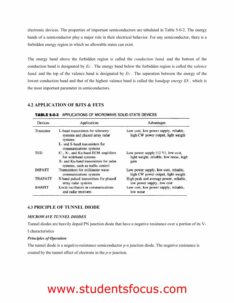
4.2 APPLICATION OF BJTS & FETS
4.3 PRICIPLE OF TUNNEL DIODE
MICROWAVE TUNNEL DIODES
Tunnel diodes are heavily doped PN junction diode that have a negative resistance over a portion of its V-
I characteristics
Principles of Operation
The tunnel diode is a negative-resistance semiconductor p-n junction diode. The negative resistance is
created by the tunnel effect of electrons in the p-n junction.
Fatima Michael College of Engineering & Technology
Fatima Michael College of Engineering & Technology
Fatima Michael College of Engineering & Technologywww.studentsfocus.com
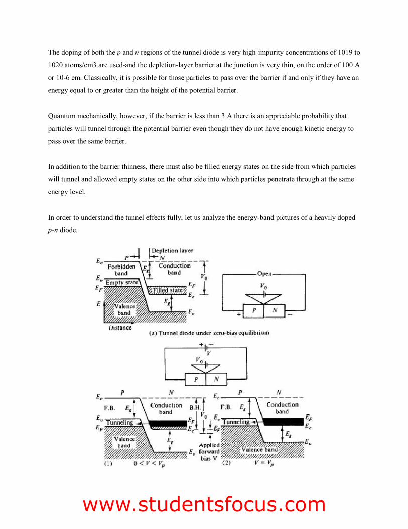
The doping of both the p and n regions of the tunnel diode is very high-impurity concentrations of 1019 to
1020 atoms/cm3 are used-and the depletion-layer barrier at the junction is very thin, on the order of 100 A
or 10-6 em. Classically, it is possible for those particles to pass over the barrier if and only if they have an
energy equal to or greater than the height of the potential barrier.
Quantum mechanically, however, if the barrier is less than 3 A there is an appreciable probability that
particles will tunnel through the potential barrier even though they do not have enough kinetic energy to
pass over the same barrier.
In addition to the barrier thinness, there must also be filled energy states on the side from which particles
will tunnel and allowed empty states on the other side into which particles penetrate through at the same
energy level.
In order to understand the tunnel effects fully, let us analyze the energy-band pictures of a heavily doped
p-n diode.
Fatima Michael College of Engineering & Technology
Fatima Michael College of Engineering & Technology
Fatima Michael College of Engineering & Technologywww.studentsfocus.com
Under open-circuit conditions or at zero-bias equilibrium, the upper levels of electron energy of both the
p type and n type are lined up at the same Fermi level as shown in Fig. 5-3-l(a).
Since there are no filled states on one side of the junction that are at the same energy level as empty
allowed states on the other side, there is no flow of charge in either direction across the junction and the
current is zero, as shown at point (a) of the volt-ampere characteristic curve of a tunnel diode in Fig.
Fatima Michael College of Engineering & Technology
Fatima Michael College of Engineering & Technology
Fatima Michael College of Engineering & Technologywww.studentsfocus.com
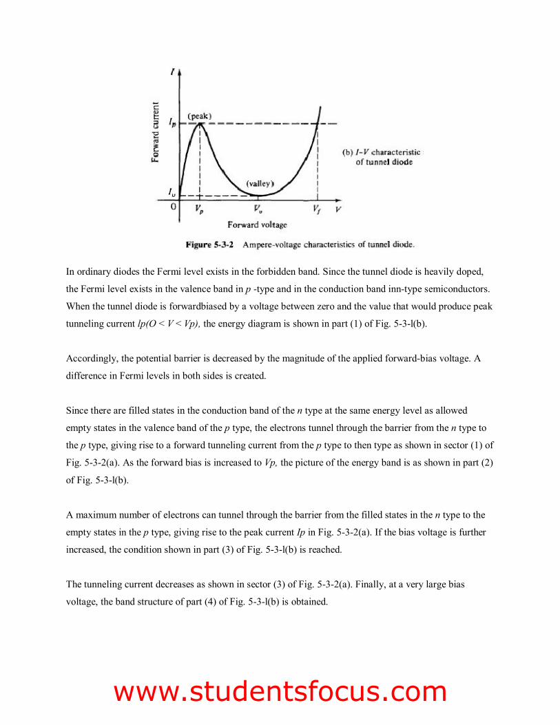
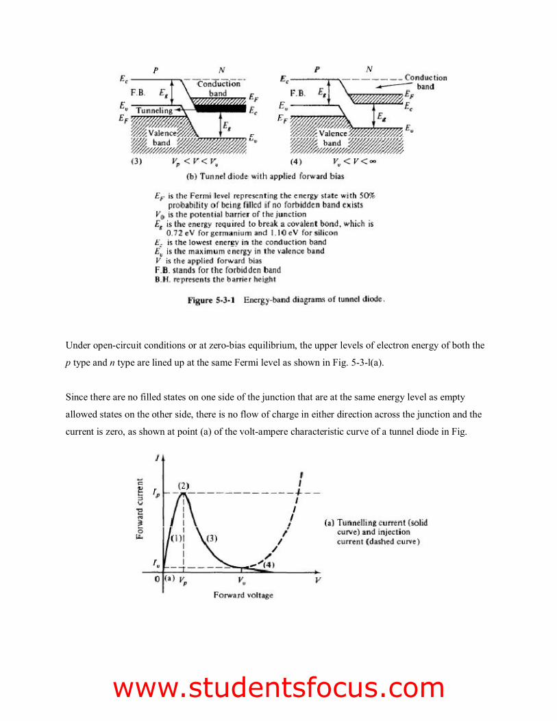
In ordinary diodes the Fermi level exists in the forbidden band. Since the tunnel diode is heavily doped,
the Fermi level exists in the valence band in p -type and in the conduction band inn-type semiconductors.
When the tunnel diode is forwardbiased by a voltage between zero and the value that would produce peak
tunneling current lp(O < V < Vp), the energy diagram is shown in part (1) of Fig. 5-3-l(b).
Accordingly, the potential barrier is decreased by the magnitude of the applied forward-bias voltage. A
difference in Fermi levels in both sides is created.
Since there are filled states in the conduction band of the n type at the same energy level as allowed
empty states in the valence band of the p type, the electrons tunnel through the barrier from the n type to
the p type, giving rise to a forward tunneling current from the p type to then type as shown in sector (1) of
Fig. 5-3-2(a). As the forward bias is increased to Vp, the picture of the energy band is as shown in part (2)
of Fig. 5-3-l(b).
A maximum number of electrons can tunnel through the barrier from the filled states in the n type to the
empty states in the p type, giving rise to the peak current Ip in Fig. 5-3-2(a). If the bias voltage is further
increased, the condition shown in part (3) of Fig. 5-3-l(b) is reached.
The tunneling current decreases as shown in sector (3) of Fig. 5-3-2(a). Finally, at a very large bias
voltage, the band structure of part (4) of Fig. 5-3-l(b) is obtained.
Fatima Michael College of Engineering & Technology
Fatima Michael College of Engineering & Technology
Fatima Michael College of Engineering & Technologywww.studentsfocus.com
Since there are now no allowed empty states in the p type at the same energy level as filled states in the n
type, no electrons can tunnel through the barrier and the tunneling current drops to zero as shown at point
(4) of Fig. 5-3-2(a).
When the forward-bias voltage V is increased above the valley voltage Vv , the ordinary injection current I
at the p-n junction starts to flow.
This injection current is increased exponentially with the forward voltage as indicated by the dashed
curve of Fig. 5-3-2(a). The total current, given by the sum of the tunneling current and the injection
current, results in the volt-ampere characteristic of the tunnel diode as shown in Fig. 5-3-2(b).
It can be seen from the figure that the total current reaches a minimum value Iv (or valley current)
somewhere in the region where the tunnel diode characteristic meets the ordinary p-n diode characteristic.
The ratio of peak current to valley current (/p!Iv) can theoretically reach 50 to 100. In practice, however,
this ratio is about 15.
4.4 VARACTOR AND STEP RECOVERY DIODE
It is a high-efficiency microwave generator capable of operating from several hundred megahertz to
several gigahertz. The basic operation of the oscillator is a semiconductor p-n junction diode reverse
biased to current densities well in excess of those encountered in normal avalanche operation.
High-peak-power diodes are typically silicon n+ -p-p+ (or p+ -n-n+) structures with then-type depletion
region width varying from 2.5 to 12.5 JLm. The doping of the depletion region is generally such that the
diodes are well "punched through" at breakdown; that is, the de electric field in the depletion region just
prior to breakdown is well above the saturated drift-velocity level. The device's p+ region is kept as thin
as possible at 2.5 to 7.5 JLm. The TRAPATT diode's diameter ranges from as small as 50 JLm for CW
operation to 750 JLm at lower frequency for high peak- power devices.
Principles of Operation
high-field avalanche zone propagates through the diode and fills the depletion layer with a dense plasma
of electrons and holes that become trapped in the low-field region behind the zone.
At point A the electric field is uniform throughout the sample and its magnitude is large but less than the value required for avalanche breakdown. The current density is expressed by The current density is expressed by
Fatima Michael College of Engineering & Technology
Fatima Michael College of Engineering & Technology
Fatima Michael College of Engineering & Technologywww.studentsfocus.com
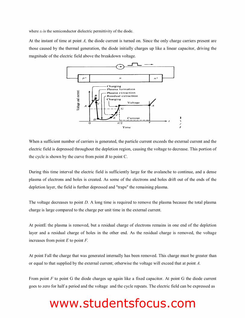
where Es is the semiconductor dielectric permittivity of the diode. At the instant of time at point A, the diode current is turned on. Since the only charge carriers present are
those caused by the thermal generation, the diode initially charges up like a linear capacitor, driving the
magnitude of the electric field above the breakdown voltage.
When a sufficient number of carriers is generated, the particle current exceeds the external current and the
electric field is depressed throughout the depletion region, causing the voltage to decrease. This portion of
the cycle is shown by the curve from point B to point C.
During this time interval the electric field is sufficiently large for the avalanche to continue, and a dense
plasma of electrons and holes is created. As some of the electrons and holes drift out of the ends of the
depletion layer, the field is further depressed and "traps" the remaining plasma.
The voltage decreases to point D. A long time is required to remove the plasma because the total plasma
charge is large compared to the charge per unit time in the external current.
At pointE the plasma is removed, but a residual charge of electrons remains in one end of the depletion
layer and a residual charge of holes in the other end. As the residual charge is removed, the voltage
increases from point E to point F.
At point Fall the charge that was generated internally has been removed. This charge must be greater than
or equal to that supplied by the external current; otherwise the voltage will exceed that at point A.
From point F to point G the diode charges up again like a fixed capacitor. At point G the diode current
goes to zero for half a period and the voltage and the cycle repeats. The electric field can be expressed as
Fatima Michael College of Engineering & Technology
Fatima Michael College of Engineering & Technology
Fatima Michael College of Engineering & Technologywww.studentsfocus.com
where NA is the doping concentration of then region and xis the distance. Thus the value of t at which the
electric field reaches Em at a given distance x into the depletion region is obtained by setting E(x, t) = Em,
yielding
Differentiation of Eq. (8-3-3) with respect to time t results in
where Vz is the avalanche-zone velocity.
the low-field mobilities, and the transit time of the carriers can become much longer than
Power Output and Efficiency
RF power is delivered by the diode to an external load when the diode is placed in a proper circuit
with a load. The main function of this circuit is to match the diode effective negative resistance to the load
at the output frequency while reactively terminating (trapping) frequencies above the oscillation
frequency in order to ensure TRAPATT operation. To date, the highest pulse power of 1.2 kW has been
obtained at 1.1 GHz (five diodes in series) [10], and the highest efficiency of 75% has been achieved at
0.6 GHz (11). Table 8-3-1 shows the current state of TRAPATT diodes
4.5 TRANSFERRED ELECTRON DEVICES
The application of two-terminal semiconductor devices at microwave frequencies has been
increased usage during the past decades. The CW, average, and peak power outputs of these
devices at higher microwave frequencies are much larger than those obtainable with the best
power transistor. The common characteristic of all active
Fatima Michael College of Engineering & Technology
Fatima Michael College of Engineering & Technology
Fatima Michael College of Engineering & Technologywww.studentsfocus.com
two-terminal solid-state devices is their negative resistance. The real part of their impedance is
negative over a range of frequencies. In a positive resistance the current through the resistance
and the voltage across it are in phase. The voltage drop across a positive resistance is positive
and a power of (/2 R) is dissipated in the resistance. In a negative resistance, however, the
current and voltage are out of phase by 180°. The voltage drop across a negative resistance is
negative, and a power of (-/ 2 R) is generated by the power supply associated with the negative
resistance. In other words, positive resistances absorb power (passive devices), whereas negative
resistances generate power (active devices). In this chapter the transferred electron devices
(TEDs) are analyzed. The differences between microwave transistors and transferred electron
devices (TEDs) are fundamental. Transistors operate with either junctions or gates, but
TEDs are bulk devices having no junctions or gates. The majority of transistors are fabricated
from elemental semiconductors, such as silicon or germanium, whereas TEDs are fabricated
from compound semiconductors, such as gallium arsenide (GaAs), indium phosphide (InP), or
cadmium telluride (CdTe). Transistors operate with "warm" electrons whose energy is not much
greater than the thermal energy (0.026 eV at room temperature) of electrons in the
semiconductor, whereas TEDs operate with "hot" electrons whose energy is very much greater
than the thermal energy. Because of these fundamental differences, the theory and technology of
transistors cannot be applied to TEDs.
4.6 GUNN DIODE
Gunn Effect:
Gun effect was first observed by GUNN in n_type GaAs bulk diode. According to GUNN, above some
critical voltage corresponding to an electric field of 2000-4000v/cm, the current in every specimen
became a fluctuating fuction of time. The frequency of oscillation was determined mainly by the
specimen and not by the external circuit.
RIDLEY-WATKINS-HILSUM (RWH} THEORY
Differential Negative Resistance
The fundamental concept of the Ridley-Watkins-Hilsum (RWH) theory is the differential negative
resistance developed in a bulk solid-state Ill-Y compound when either a voltage (or electric field) or a
current is applied to the terminals of the sample.
There are two modes of negative-resistance devices:
Fatima Michael College of Engineering & Technology
Fatima Michael College of Engineering & Technology
Fatima Michael College of Engineering & Technologywww.studentsfocus.com
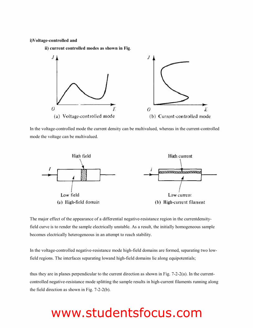
i)Voltage-controlled and
ii) current controlled modes as shown in Fig.
In the voltage-controlled mode the current density can be multivalued, whereas in the current-controlled
mode the voltage can be multivalued.
The major effect of the appearance of a differential negative-resistance region in the currentdensity-
field curve is to render the sample electrically unstable. As a result, the initially homogeneous sample
becomes electrically heterogeneous in an attempt to reach stability.
In the voltage-controlled negative-resistance mode high-field domains are formed, separating two low-
field regions. The interfaces separating lowand high-field domains lie along equipotentials;
thus they are in planes perpendicular to the current direction as shown in Fig. 7-2-2(a). In the current-
controlled negative-resistance mode splitting the sample results in high-current filaments running along
the field direction as shown in Fig. 7-2-2(b).
Fatima Michael College of Engineering & Technology
Fatima Michael College of Engineering & Technology
Fatima Michael College of Engineering & Technologywww.studentsfocus.com
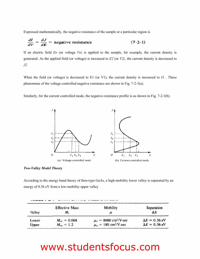
Expressed mathematically, the negative resistance of the sample at a particular region is
If an electric field Eo (or voltage Vo) is applied to the sample, for example, the current density is
generated. As the applied field (or voltage) is increased to E2 (or V2), the current density is decreased to
J2.
When the field (or voltage) is decreased to E1 (or V1), the current density is increased to J1 . These
phenomena of the voltage controlled negative resistance are shown in Fig. 7-2-3(a).
Similarly, for the current controlled mode, the negative-resistance profile is as shown in Fig. 7-2-3(b).
Two-Valley Model Theory
According to the energy band theory of then-type GaAs, a high-mobility lower valley is separated by an
energy of 0.36 eV from a low-mobility upper valley
Fatima Michael College of Engineering & Technology
Fatima Michael College of Engineering & Technology
Fatima Michael College of Engineering & Technologywww.studentsfocus.com
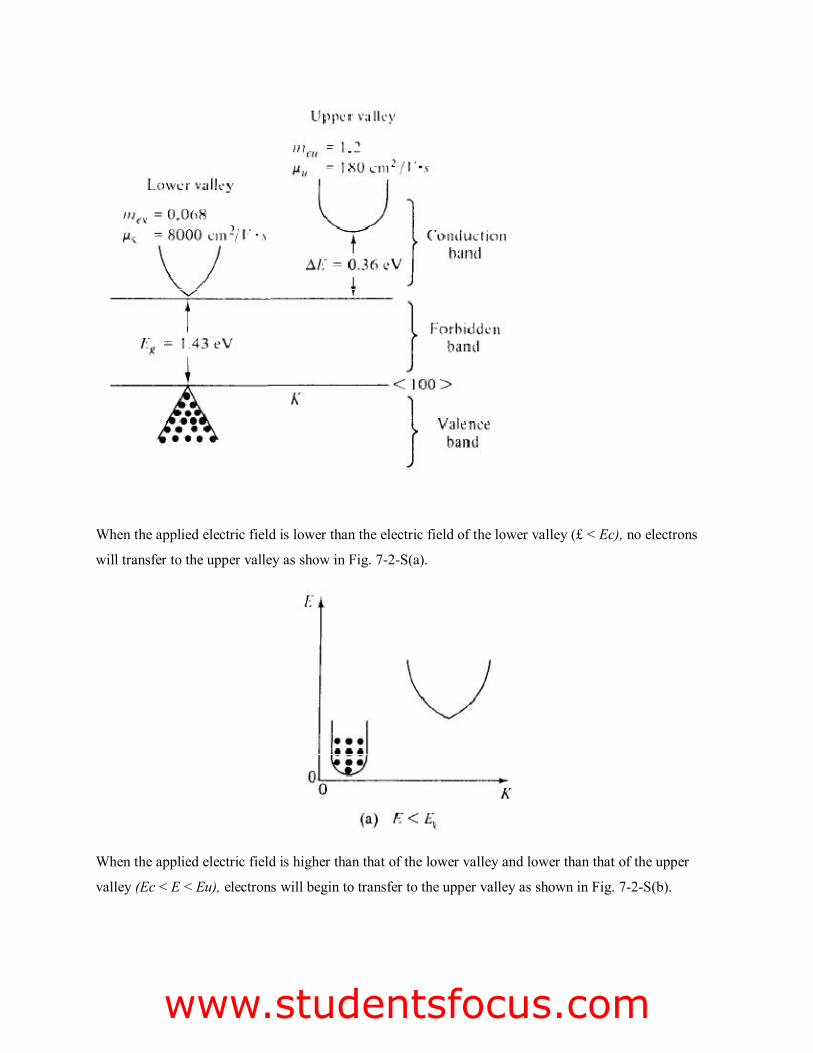
When the applied electric field is lower than the electric field of the lower valley (£ < Ec), no electrons
will transfer to the upper valley as show in Fig. 7-2-S(a).
When the applied electric field is higher than that of the lower valley and lower than that of the upper
valley (Ec < E < Eu), electrons will begin to transfer to the upper valley as shown in Fig. 7-2-S(b).
Fatima Michael College of Engineering & Technology
Fatima Michael College of Engineering & Technology
Fatima Michael College of Engineering & Technologywww.studentsfocus.com
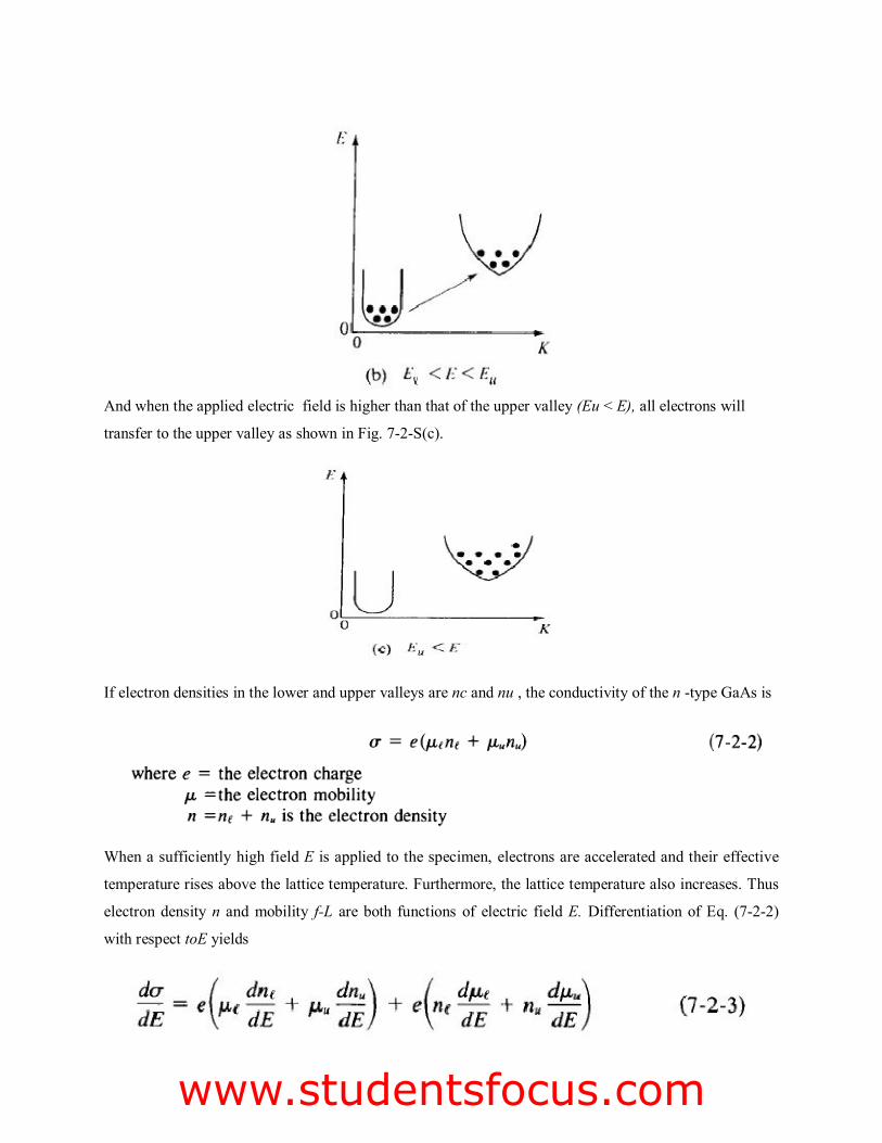
And when the applied electric field is higher than that of the upper valley (Eu < E), all electrons will
transfer to the upper valley as shown in Fig. 7-2-S(c).
If electron densities in the lower and upper valleys are nc and nu , the conductivity of the n -type GaAs is
When a sufficiently high field E is applied to the specimen, electrons are accelerated and their effective
temperature rises above the lattice temperature. Furthermore, the lattice temperature also increases. Thus
electron density n and mobility f-L are both functions of electric field E. Differentiation of Eq. (7-2-2)
with respect toE yields
Fatima Michael College of Engineering & Technology
Fatima Michael College of Engineering & Technology
Fatima Michael College of Engineering & Technologywww.studentsfocus.com
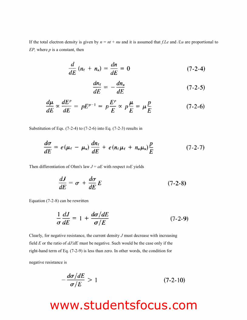
If the total electron density is given by n = nt + nu and it is assumed that f.Le and /Lu are proportional to
EP, where p is a constant, then
Substitution of Eqs. (7-2-4) to (7-2-6) into Eq. (7-2-3) results in
Then differentiation of Ohm's law J = aE with respect toE yields
Equation (7-2-8) can be rewritten
Clearly, for negative resistance, the current density J must decrease with increasing
field E or the ratio of dJ!dE must be negative. Such would be the case only if the
right-hand term of Eq. (7-2-9) is less than zero. In other words, the condition for
negative resistance is
Fatima Michael College of Engineering & Technology
Fatima Michael College of Engineering & Technology
Fatima Michael College of Engineering & Technologywww.studentsfocus.com
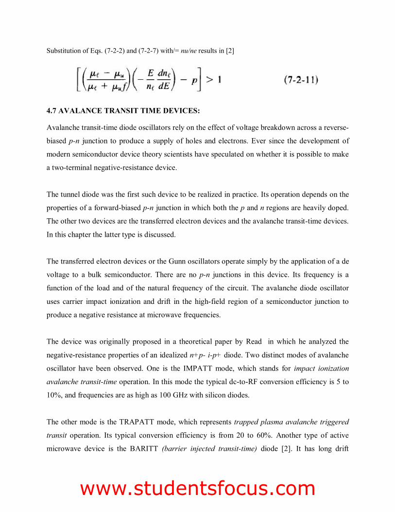
Substitution of Eqs. (7-2-2) and (7-2-7) with/= nu/ne results in [2]
4.7 AVALANCE TRANSIT TIME DEVICES:
Avalanche transit-time diode oscillators rely on the effect of voltage breakdown across a reverse-
biased p-n junction to produce a supply of holes and electrons. Ever since the development of
modern semiconductor device theory scientists have speculated on whether it is possible to make
a two-terminal negative-resistance device.
The tunnel diode was the first such device to be realized in practice. Its operation depends on the
properties of a forward-biased p-n junction in which both the p and n regions are heavily doped.
The other two devices are the transferred electron devices and the avalanche transit-time devices.
In this chapter the latter type is discussed.
The transferred electron devices or the Gunn oscillators operate simply by the application of a de
voltage to a bulk semiconductor. There are no p-n junctions in this device. Its frequency is a
function of the load and of the natural frequency of the circuit. The avalanche diode oscillator
uses carrier impact ionization and drift in the high-field region of a semiconductor junction to
produce a negative resistance at microwave frequencies.
The device was originally proposed in a theoretical paper by Read in which he analyzed the
negative-resistance properties of an idealized n+p- i-p+ diode. Two distinct modes of avalanche
oscillator have been observed. One is the IMPATT mode, which stands for impact ionization
avalanche transit-time operation. In this mode the typical dc-to-RF conversion efficiency is 5 to
10%, and frequencies are as high as 100 GHz with silicon diodes.
The other mode is the TRAPATT mode, which represents trapped plasma avalanche triggered
transit operation. Its typical conversion efficiency is from 20 to 60%. Another type of active
microwave device is the BARITT (barrier injected transit-time) diode [2]. It has long drift
Fatima Michael College of Engineering & Technology
Fatima Michael College of Engineering & Technology
Fatima Michael College of Engineering & Technologywww.studentsfocus.com

regions similar to those of IMPATT diodes. The carriers traversing the drift regions of BARITT
diodes, however, are generated by minority carrier injection from forward-biased junctions rather
than being extracted from the plasma of an avalanche region. Several different structures have
been operated as BARITT diodes, such as p-n-p, p-n-v-p, p-n-metal, and metal-nmetal. BARITT
diodes have low noise figures of 15 dB, but their bandwidth is relatively narrow with low output
power.
4.8 IMPATT AND TRAPATT DIODE:
Physical Structures
A theoretical Read diode made of ann+ -p-i-p+ or p+ -n-i-n+ structure has been analyzed. Its basic
physical mechanism is the interaction of the impact ionization avalanche and the transit time of charge
carriers. Hence the Read-type diodes are called IMPATT diodes. These diodes exhibit a differential
negative resistance by two effects:
1)The impact ionization avalanche effect, which causes the carrier current lo(t) and the ac voltage to be
out of phase by 90°
2) The transit-time effect, which further delays the external current l,(t) relative to the ac voltage by 90°
The first IMPATT operation as reported by Johnston et al. [4] in 1965, however, was obtained from a
simple p-n junction. The first real Read-type IMPATT diode was reported by Lee et al. [3], as described
previously.
From the small-signal theory developed by Gilden [5] it has been confirmed that a negative resistance of
the IMPATT diode can be obtained from a junction diode with any doping profile.
Many IMPATT diodes consist of a high doping avalanching region followed by a drift region where the
field is low enough that the carriers can traverse through it without avalanching.
The Read diode is the basic type in the IMPATT diode family. The others are the one-sided abrupt p-n
junction, the linearly graded p-n junction (or double-drift region), and the p-i-n diode, all of which are
shown in Fig. 8-2-1.
Fatima Michael College of Engineering & Technology
Fatima Michael College of Engineering & Technology
Fatima Michael College of Engineering & Technologywww.studentsfocus.com
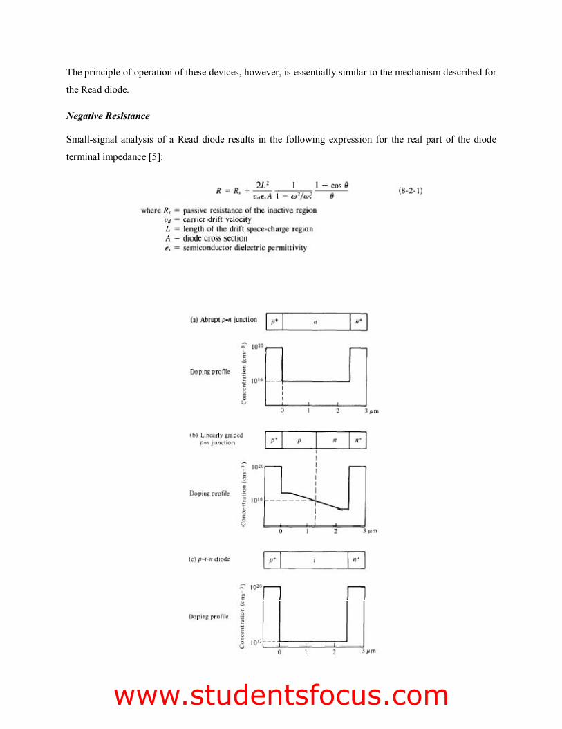
The principle of operation of these devices, however, is essentially similar to the mechanism described for
the Read diode.
Negative Resistance
Small-signal analysis of a Read diode results in the following expression for the real part of the diode
terminal impedance [5]:
Fatima Michael College of Engineering & Technology
Fatima Michael College of Engineering & Technology
Fatima Michael College of Engineering & Technologywww.studentsfocus.com
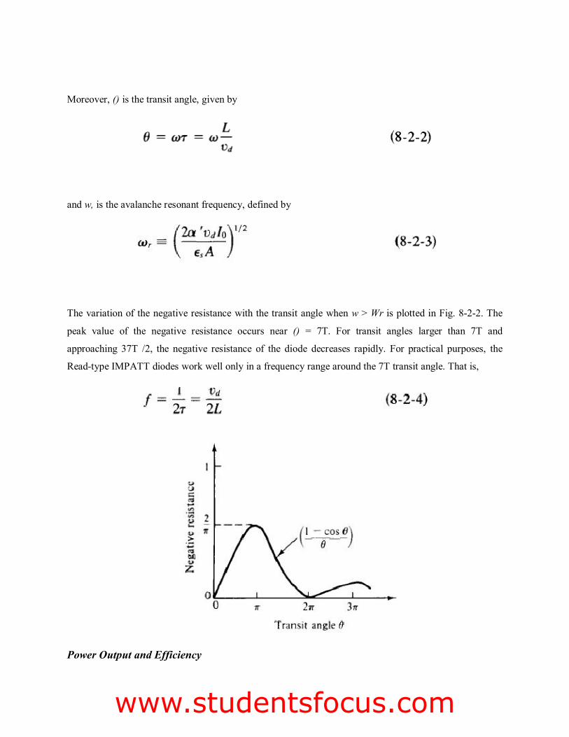
Moreover, () is the transit angle, given by
and w, is the avalanche resonant frequency, defined by
The variation of the negative resistance with the transit angle when w > Wr is plotted in Fig. 8-2-2. The
peak value of the negative resistance occurs near () = 7T. For transit angles larger than 7T and
approaching 37T /2, the negative resistance of the diode decreases rapidly. For practical purposes, the
Read-type IMPATT diodes work well only in a frequency range around the 7T transit angle. That is,
Power Output and Efficiency
Fatima Michael College of Engineering & Technology
Fatima Michael College of Engineering & Technology
Fatima Michael College of Engineering & Technologywww.studentsfocus.com
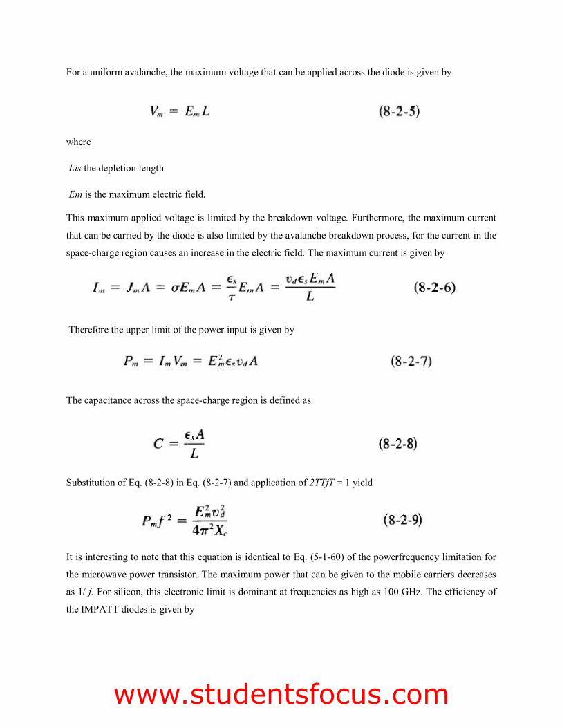
For a uniform avalanche, the maximum voltage that can be applied across the diode is given by
where
Lis the depletion length
Em is the maximum electric field.
This maximum applied voltage is limited by the breakdown voltage. Furthermore, the maximum current
that can be carried by the diode is also limited by the avalanche breakdown process, for the current in the
space-charge region causes an increase in the electric field. The maximum current is given by
Therefore the upper limit of the power input is given by
The capacitance across the space-charge region is defined as
Substitution of Eq. (8-2-8) in Eq. (8-2-7) and application of 2TTfT = 1 yield
It is interesting to note that this equation is identical to Eq. (5-1-60) of the powerfrequency limitation for
the microwave power transistor. The maximum power that can be given to the mobile carriers decreases
as 1/ f. For silicon, this electronic limit is dominant at frequencies as high as 100 GHz. The efficiency of
the IMPATT diodes is given by
Fatima Michael College of Engineering & Technology
Fatima Michael College of Engineering & Technology
Fatima Michael College of Engineering & Technologywww.studentsfocus.com
4.9 PARAMETRIC DEVICES:
Parametric Amplifiers
In a super heterodyne receiver a radio frequency signal may be mixed with a signal from the local
oscillator in a nonlinear circuit (the mixer) to generate the sum and difference frequencies.
In a parametric amplifier the local oscillator is replaced by a pumping generator such as a reflex klystron
and the nonlinear element by a time varying capacitor such as a varactor diode (or inductor) as shown in
Fig.
In Fig. 8-5-2, the signal frequency !s and the pump frequency f, are mixed in the nonlinear capacitor C.
Accordingly, a voltage of the fundamental frequencies !s andf, as well as the sum and the difference
frequencies mfp ± nfs appears across C.
If a resistive load is connected across the terminals of the idler circuit, an output voltage can be generated
across the load at the output frequency fa . The output circuit, which does not require external excitation,
is called the idler circuit.
The output (or idler) frequency fa in the idler circuit is expressed as the sum and the difference
frequencies of the signal frequency fs and the pump frequency fp,. That is,
where m and n are positive integers from zero to infinity.
If fo > fs , the device is called a parametric up-converter. Conversely, if
fo < fs, the device is known as a parametric down-converter.
Fatima Michael College of Engineering & Technology
Fatima Michael College of Engineering & Technology
Fatima Michael College of Engineering & Technologywww.studentsfocus.com
Parametric up-converter.
A parametric up-converter has the following properties:
1) The ouptut frequency is equal to the sum of the signal frequency and the pump frequency.
2) There is no power flow in the parametric device at frequencies other than the
signal, pump, and output frequencies.
Power Gain.
When these two conditions are satisfied, the maximum power gain of a parametric up-converter [21] is
expressed as
Moreover, Rd is the series resistance of a p-n junction diode and yQ is the figure of merit for the nonlinear
capacitor. The quantity of may be regarded as a gain-degradation factor. As Rd
approaches zero, the figure of merit yQ goes to infinity and the gain-degradation factor becomes equal to
unity. As a result, the power gain of a parametric up-converter for a lossless diode is equal to !ol Is ,
Fatima Michael College of Engineering & Technology
Fatima Michael College of Engineering & Technology
Fatima Michael College of Engineering & Technologywww.studentsfocus.com
which is predicted by the Manley-Rowe relations as shown in Eq. (8-5-27). In a typical microwave diode
yQ could be equal to 10. If the maximum gain given by Eq. (8-5-30) is 7.3 dB.
Noise Figure.
One advantage of the parametric amplifier over the transistor amplifier is its low-noise figure because a
pure reactance does not contribute thermal noise to the circuit. The noise figure F for a parametric up-
converter [21] is given by
Bandwidth.
The bandwidth of a parametric up-converter is related to the gain-degradation factor of the merit figure
and the ratio of the signal frequency to the output frequency. The bandwidth equation [21] is given by
If fol is = 10 and y = 0.2, the bandwidth (BW) is equal to 1.264.
Parametric down-converter.
The down-conversion gain (actually a loss) is given by
Negative-resistance parametric amplifier.
If a significant portion of power flows only at the signal frequency Is , the pump frequency fp , and the
idler frequency j; , a regenerative condition with the possibility of oscillation at both the signal frequency
and the idler frequency will occur.
The idler frequency is
When the mode operates below the oscillation threshold, the device behaves as a bilateral negative-
resistance parametric amplifier.
Fatima Michael College of Engineering & Technology
Fatima Michael College of Engineering & Technology
Fatima Michael College of Engineering & Technologywww.studentsfocus.com
Power Gain.
The output power is taken from the resistance R; at a frequency j; , and the conversion gain from Is to j;
[21] is given by
Noise Figure. The optimum noise figure of a negative-resistance parametric amplifier [21] is expressed as
The optimum noise figure of a negative-resistance parametric amplifier [21] is expressed as
Bandwidth.
The maximum gain bandwidth of a negative-resistance parametric amplifier [21] is given by
Degenerate parametric amplifier.
The degenerate parametric amplifier or oscillator is defined as a negative-resistance amplifier with the
signal frequency equal to the idler frequency.
Power Gain and Bandwidth.
Fatima Michael College of Engineering & Technology
Fatima Michael College of Engineering & Technology
Fatima Michael College of Engineering & Technologywww.studentsfocus.com
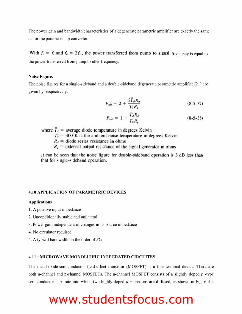
The power gain and bandwidth characteristics of a degenerate parametric amplifier are exactly the same
as for the parametric up converter.
frequency is equal to
the power transferred from pump to idler frequency.
Noise Figure.
The noise figures for a single-sideband and a double-sideband degenerate parametric amplifier [21] are
given by, respectively,
4.10 APPLICATION OF PARAMETRIC DEVICES
Applications
1. A positive input impedance
2. Unconditionally stable and unilateral
3. Power gain independent of changes in its source impedance
4. No circulator required
5. A typical bandwidth on the order of 5%
4.11 : MICROWAVE MONOLITHIC INTEGRATED CIRCUITES
The metal-oxide-semiconductor field-effect transistor (MOSFET) is a four-terminal device. There are
both n-channel and p-channel MOSFETs. The n-channel MOSFET consists of a slightly doped p -type
semiconductor substrate into which two highly doped n + sections are diffused, as shown in Fig. 6-4-l.
Fatima Michael College of Engineering & Technology
Fatima Michael College of Engineering & Technology
Fatima Michael College of Engineering & Technologywww.studentsfocus.com
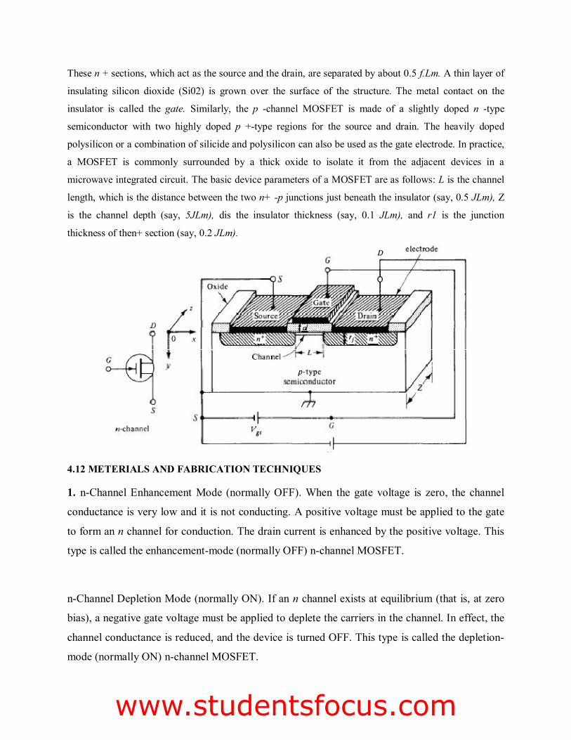
These n + sections, which act as the source and the drain, are separated by about 0.5 f.Lm. A thin layer of
insulating silicon dioxide (Si02) is grown over the surface of the structure. The metal contact on the
insulator is called the gate. Similarly, the p -channel MOSFET is made of a slightly doped n -type
semiconductor with two highly doped p +-type regions for the source and drain. The heavily doped
polysilicon or a combination of silicide and polysilicon can also be used as the gate electrode. In practice,
a MOSFET is commonly surrounded by a thick oxide to isolate it from the adjacent devices in a
microwave integrated circuit. The basic device parameters of a MOSFET are as follows: L is the channel
length, which is the distance between the two n+ -p junctions just beneath the insulator (say, 0.5 JLm), Z
is the channel depth (say, 5JLm), dis the insulator thickness (say, 0.1 JLm), and r1 is the junction
thickness of then+ section (say, 0.2 JLm).
4.12 METERIALS AND FABRICATION TECHNIQUES
1. n-Channel Enhancement Mode (normally OFF). When the gate voltage is zero, the channel
conductance is very low and it is not conducting. A positive voltage must be applied to the gate
to form an n channel for conduction. The drain current is enhanced by the positive voltage. This
type is called the enhancement-mode (normally OFF) n-channel MOSFET.
n-Channel Depletion Mode (normally ON). If an n channel exists at equilibrium (that is, at zero
bias), a negative gate voltage must be applied to deplete the carriers in the channel. In effect, the
channel conductance is reduced, and the device is turned OFF. This type is called the depletion-
mode (normally ON) n-channel MOSFET.
Fatima Michael College of Engineering & Technology
Fatima Michael College of Engineering & Technology
Fatima Michael College of Engineering & Technologywww.studentsfocus.com
p -Channel Enhancement Mode (normally OFF). A negative voltage must be applied to the gate
to induce a p channel for conduction. This type is called the enhancement-mode (normally OFF)
p-channel MOSFET.
p -Channel Depletion Mode (normally ON). A positive voltage must be applied to the gate to
deplete the carriers in the channel for nonconduction. This type is called the depletion-mode
(normally ON) p-channel MOSFET.
Fatima Michael College of Engineering & Technology
Fatima Michael College of Engineering & Technology
Fatima Michael College of Engineering & Technologywww.studentsfocus.com
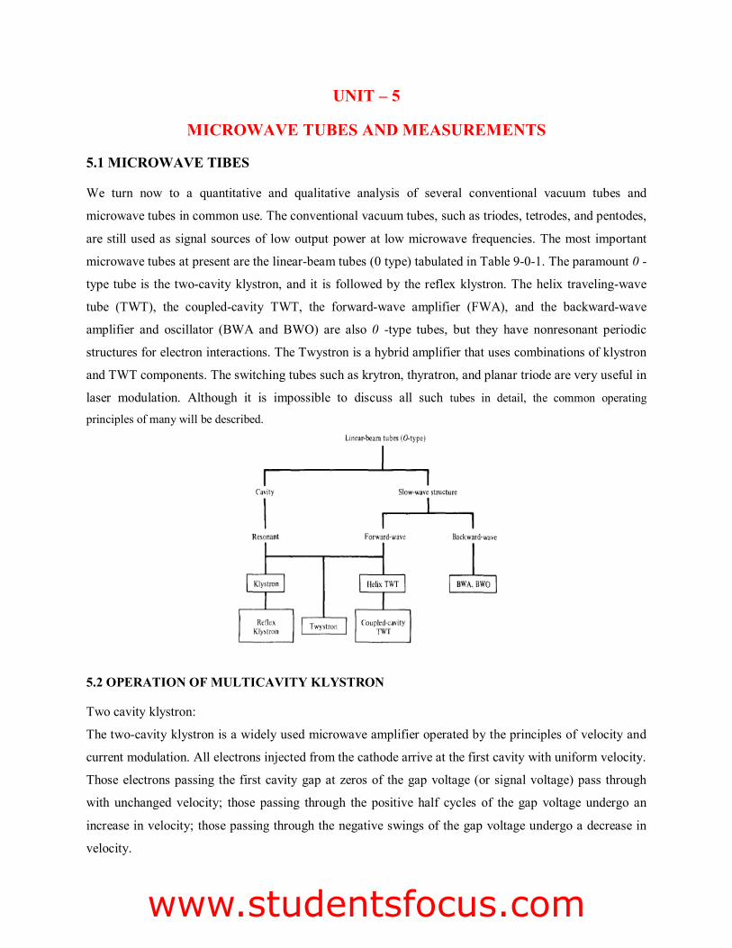
UNIT – 5
MICROWAVE TUBES AND MEASUREMENTS
5.1 MICROWAVE TIBES
We turn now to a quantitative and qualitative analysis of several conventional vacuum tubes and
microwave tubes in common use. The conventional vacuum tubes, such as triodes, tetrodes, and pentodes,
are still used as signal sources of low output power at low microwave frequencies. The most important
microwave tubes at present are the linear-beam tubes (0 type) tabulated in Table 9-0-1. The paramount 0 -
type tube is the two-cavity klystron, and it is followed by the reflex klystron. The helix traveling-wave
tube (TWT), the coupled-cavity TWT, the forward-wave amplifier (FWA), and the backward-wave
amplifier and oscillator (BWA and BWO) are also 0 -type tubes, but they have nonresonant periodic
structures for electron interactions. The Twystron is a hybrid amplifier that uses combinations of klystron
and TWT components. The switching tubes such as krytron, thyratron, and planar triode are very useful in
laser modulation. Although it is impossible to discuss all such tubes in detail, the common operating
principles of many will be described.
5.2 OPERATION OF MULTICAVITY KLYSTRON
Two cavity klystron:
The two-cavity klystron is a widely used microwave amplifier operated by the principles of velocity and
current modulation. All electrons injected from the cathode arrive at the first cavity with uniform velocity.
Those electrons passing the first cavity gap at zeros of the gap voltage (or signal voltage) pass through
with unchanged velocity; those passing through the positive half cycles of the gap voltage undergo an
increase in velocity; those passing through the negative swings of the gap voltage undergo a decrease in
velocity.
Fatima Michael College of Engineering & Technology
Fatima Michael College of Engineering & Technology
Fatima Michael College of Engineering & Technologywww.studentsfocus.com
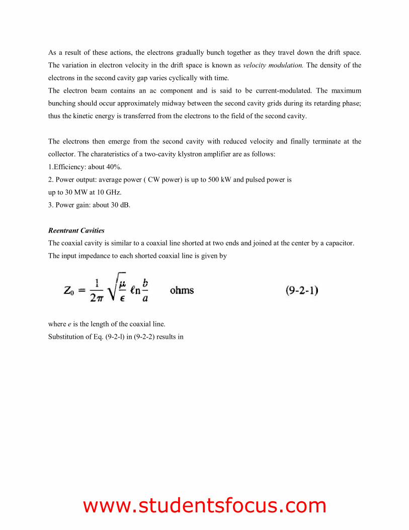
As a result of these actions, the electrons gradually bunch together as they travel down the drift space.
The variation in electron velocity in the drift space is known as velocity modulation. The density of the
electrons in the second cavity gap varies cyclically with time.
The electron beam contains an ac component and is said to be current-modulated. The maximum
bunching should occur approximately midway between the second cavity grids during its retarding phase;
thus the kinetic energy is transferred from the electrons to the field of the second cavity.
The electrons then emerge from the second cavity with reduced velocity and finally terminate at the
collector. The charateristics of a two-cavity klystron amplifier are as follows:
1.Efficiency: about 40%.
2. Power output: average power ( CW power) is up to 500 kW and pulsed power is
up to 30 MW at 10 GHz.
3. Power gain: about 30 dB.
Reentrant Cavities
The coaxial cavity is similar to a coaxial line shorted at two ends and joined at the center by a capacitor.
The input impedance to each shorted coaxial line is given by
where e is the length of the coaxial line.
Substitution of Eq. (9-2-l) in (9-2-2) results in
Fatima Michael College of Engineering & Technology
Fatima Michael College of Engineering & Technology
Fatima Michael College of Engineering & Technologywww.studentsfocus.com
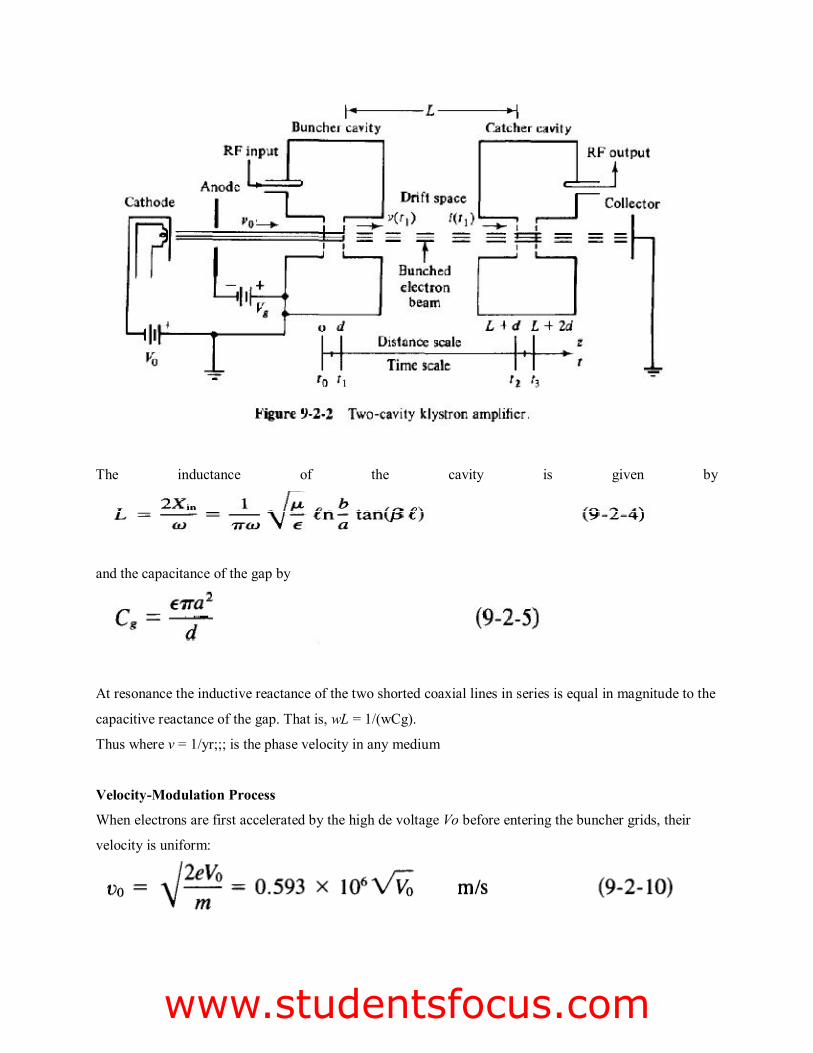
The inductance of the cavity is given by
and the capacitance of the gap by
At resonance the inductive reactance of the two shorted coaxial lines in series is equal in magnitude to the
capacitive reactance of the gap. That is, wL = 1/(wCg).
Thus where v = 1/yr;;; is the phase velocity in any medium
Velocity-Modulation Process
When electrons are first accelerated by the high de voltage Vo before entering the buncher grids, their
velocity is uniform:
Fatima Michael College of Engineering & Technology
Fatima Michael College of Engineering & Technology
Fatima Michael College of Engineering & Technologywww.studentsfocus.com

In Eq. (9-2-10) it is assumed that electrons leave the cathode with zero velocity. When a microwave
signal is applied to the input terminal, the gap voltage between the buncher grids appears as
where V1 is the amplitude of the signal and V1 << Vo is assumed.
In order to find the modulated velocity in the buncher cavity in terms of either the entering time to or the
exiting time t1 and the gap transit angle 88 as shown in Fig. 9-2-2 it is necessary to determine the average
microwave voltage in the buncher gap as indicated in Fig. 9-2-6. Since V1 << Vo , the average transit
time through the buncher gap distance d is
Fatima Michael College of Engineering & Technology
Fatima Michael College of Engineering & Technology
Fatima Michael College of Engineering & Technologywww.studentsfocus.com
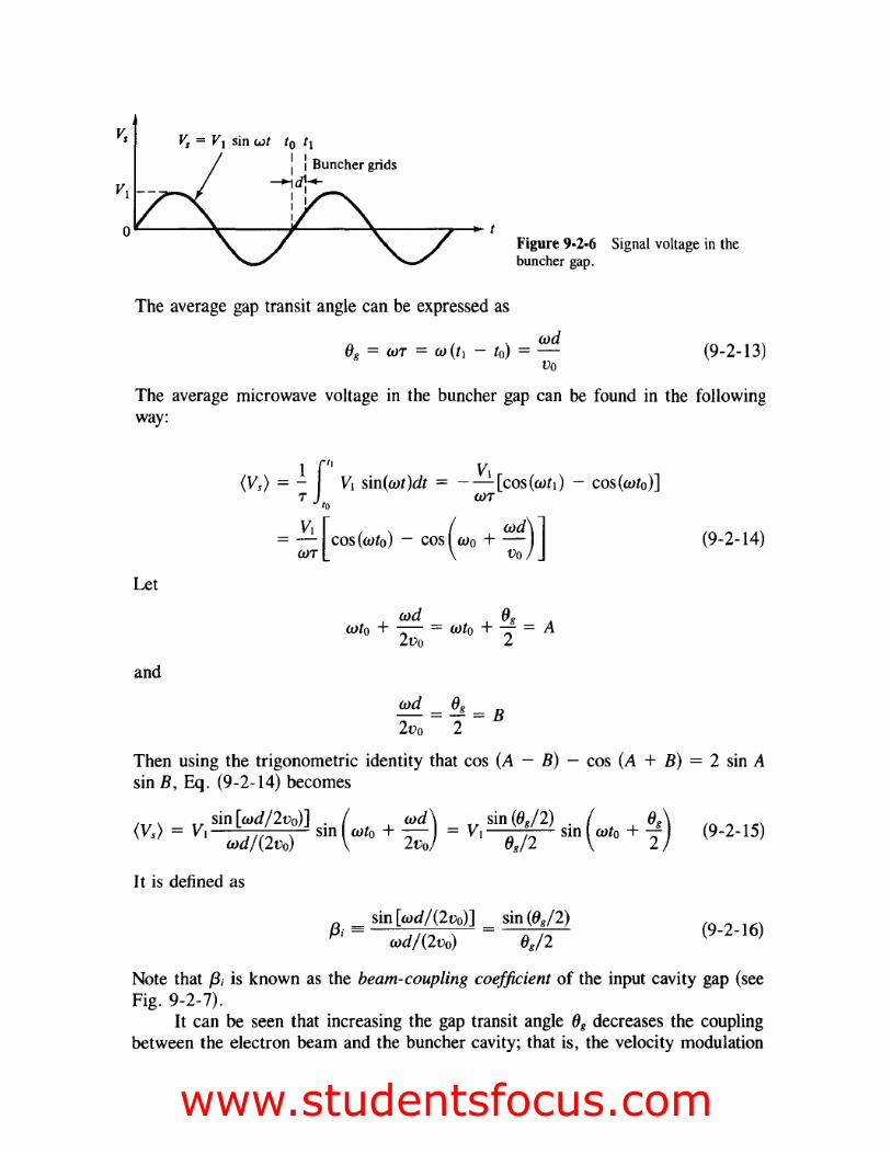
Fatima Michael College of Engineering & Technology
Fatima Michael College of Engineering & Technology
Fatima Michael College of Engineering & Technologywww.studentsfocus.com

It can be seen that increasing the gap transit angle 08 decreases the coupling between the electron beam
and the buncher cavity; that is, the velocity modulation of the beam for a given microwave signal is
decreased. Immediately after velocity modulation, the exit velocity from the buncher gap is given by
Bunching Process
Once the electrons leave the buncher cavity, they drift with a velocity given by Eq. (9-2-19) or (9-2-20)
along in the field-free space between the two cavities. The effect of velocity modulation produces
bunching of the electron beam-or current modulation.
The electrons that pass the buncher at Vs = 0 travel through with unchanged velocity vo and become the
bunching center. Those electrons that pass the buncher cavity during the positive half cycles of the
microwave input voltage Vs travel faster than the electrons that passed the gap when Vs = 0. Those
electrons that pass the buncher cavity during the negative half cycles of the voltage Vs travel slower than
the electrons that passed the gap when Vs = 0. At a distance of !:J..L along the beam from the buncher
Fatima Michael College of Engineering & Technology
Fatima Michael College of Engineering & Technology
Fatima Michael College of Engineering & Technologywww.studentsfocus.com
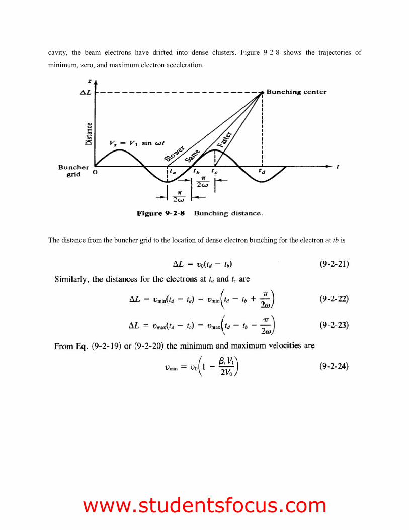
cavity, the beam electrons have drifted into dense clusters. Figure 9-2-8 shows the trajectories of
minimum, zero, and maximum electron acceleration.
The distance from the buncher grid to the location of dense electron bunching for the electron at tb is
Fatima Michael College of Engineering & Technology
Fatima Michael College of Engineering & Technology
Fatima Michael College of Engineering & Technologywww.studentsfocus.com
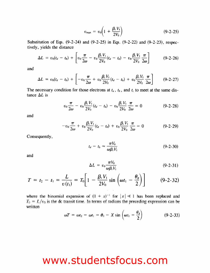
Fatima Michael College of Engineering & Technology
Fatima Michael College of Engineering & Technology
Fatima Michael College of Engineering & Technologywww.studentsfocus.com
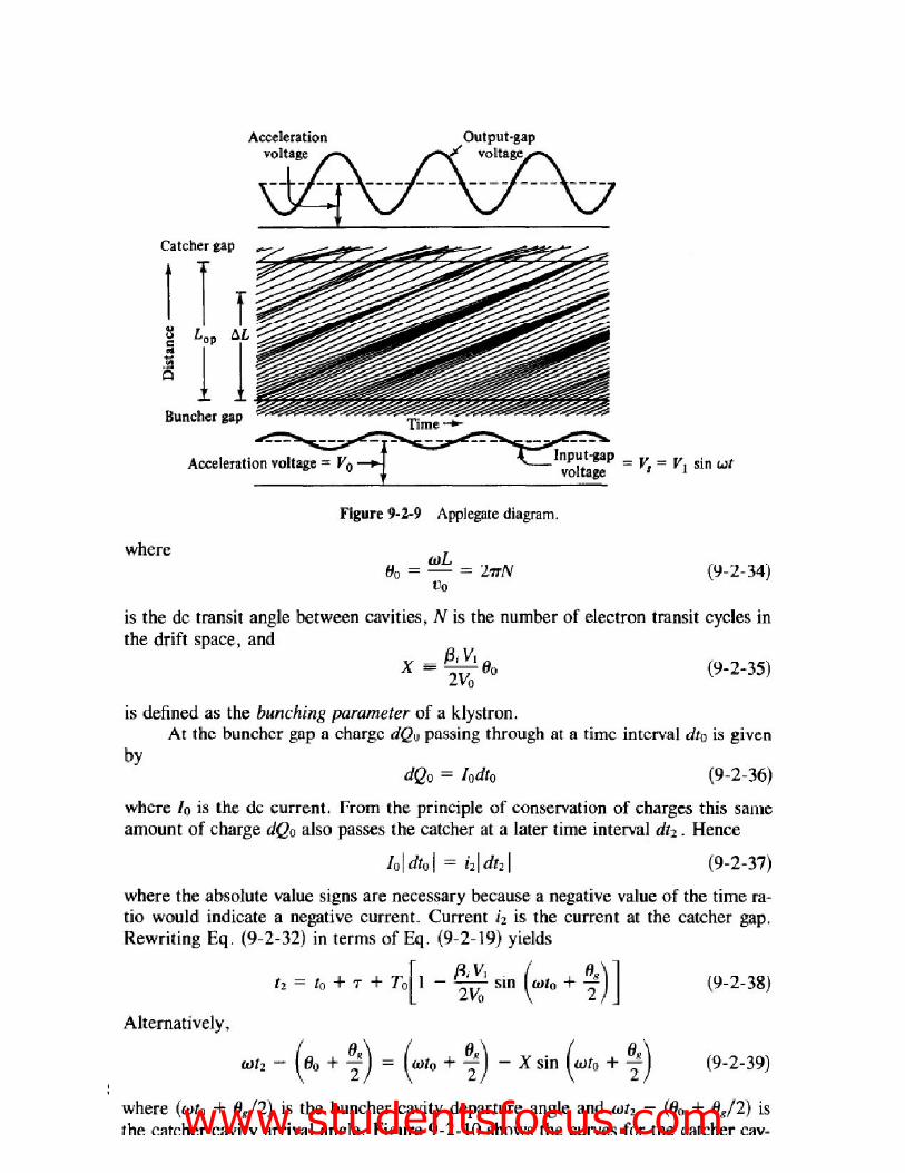
SCE 85 ECE
Fatima Michael College of Engineering & Technology
Fatima Michael College of Engineering & Technology
Fatima Michael College of Engineering & Technologywww.studentsfocus.com
5.3 REFLUX KLYSTRON
If a fraction of the output power is fed back to the input cavity and if the loop gain has a magnitude of
unity with a phase shift of multiple 27T, the klystron will oscillate. However, a two-cavity klystron
oscillator is usually not constructed because, when the oscillation frequency is varied, the resonant
frequency of each cavity and the feedback path phase shift must be readjusted for a positive feedback.
The reflex klystron is a single-cavity klystron that overcomes the disadvantages of the twocavity klystron
oscillator. It is a low-power generator of 10 to 500-mW output at a frequency range of I to 25 GHz. The
efficiency is about 20 to 30%. This type is widely used in the laboratory for microwave measurements
and in microwave receivers as local oscillators in commercial, military, and airborne Doppler radars as
well as missiles.
The theory of the two-cavity klystron can be applied to the nalysis of the reflex klystron with slight
modification. A schematic diagram of the reflex klystron is shown in Fig. 9-4-1.
Fatima Michael College of Engineering & Technology
Fatima Michael College of Engineering & Technology
Fatima Michael College of Engineering & Technologywww.studentsfocus.com

The electron beam injected from the cathode is first velocity-modulated by the cavity-gap voltage. Some
electrons accelerated by the accelerating field enter therepeller space with greater velocity than those with
unchanged velocity. Some electrons decelerated by the retarding field enter the repeller region with less
velocity.
All electrons turned around by the repeller voltage then pass through the cavity gap in bunches that occur
once per cycle. On their return journey the bunched electrons pass through the gap during the retarding
phase of the alternating field and give up their kinetic energy to the electromagnetic energy of the field in
the cavity. Oscillator output energy is then taken from the cavity. The electrons are finally collected by
the walls of the cavity or other grounded metal parts of the tube. Figure 9-4-2 shows an Applegate
diagram for the 1~ mode of a reflex klystron.
Velocity Modulation
The analysis of a reflex klystron is similar to that of a two-cavity klystron. For simplicity, the effect of
space-charge forces on the electron motion will again be neglected. The electron entering the cavity gap
from the cathode at z = 0 and time to is assumed to have uniform velocity
The same electron leaves the cavity gap at z = d at time ft with velocity
This expression is identical to Eq. (9-2-17), for the problems up to this point are identical to those of a
two-cavity klystron amplifier. The same electron is forced back to the cavity z = d and time tz by the
retarding electric field E, which is given by
This retarding field E is assumed to be constant in the z direction. The force equation for one electron in
the repeller region is
Fatima Michael College of Engineering & Technology
Fatima Michael College of Engineering & Technology
Fatima Michael College of Engineering & Technologywww.studentsfocus.com
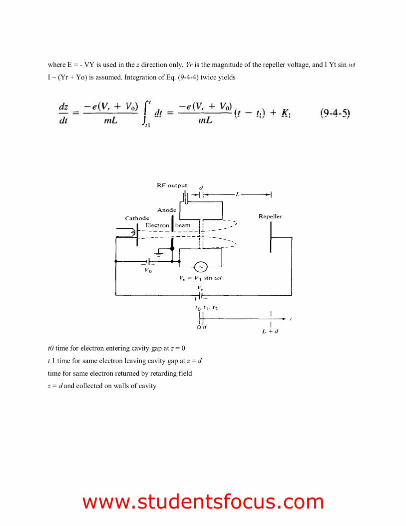
where E = - VY is used in the z direction only, Yr is the magnitude of the repeller voltage, and I Yt sin wt
I ~ (Yr + Yo) is assumed. Integration of Eq. (9-4-4) twice yields
t0 time for electron entering cavity gap at z = 0
t 1 time for same electron leaving cavity gap at z = d
time for same electron returned by retarding field
z = d and collected on walls of cavity
Fatima Michael College of Engineering & Technology
Fatima Michael College of Engineering & Technology
Fatima Michael College of Engineering & Technologywww.studentsfocus.com
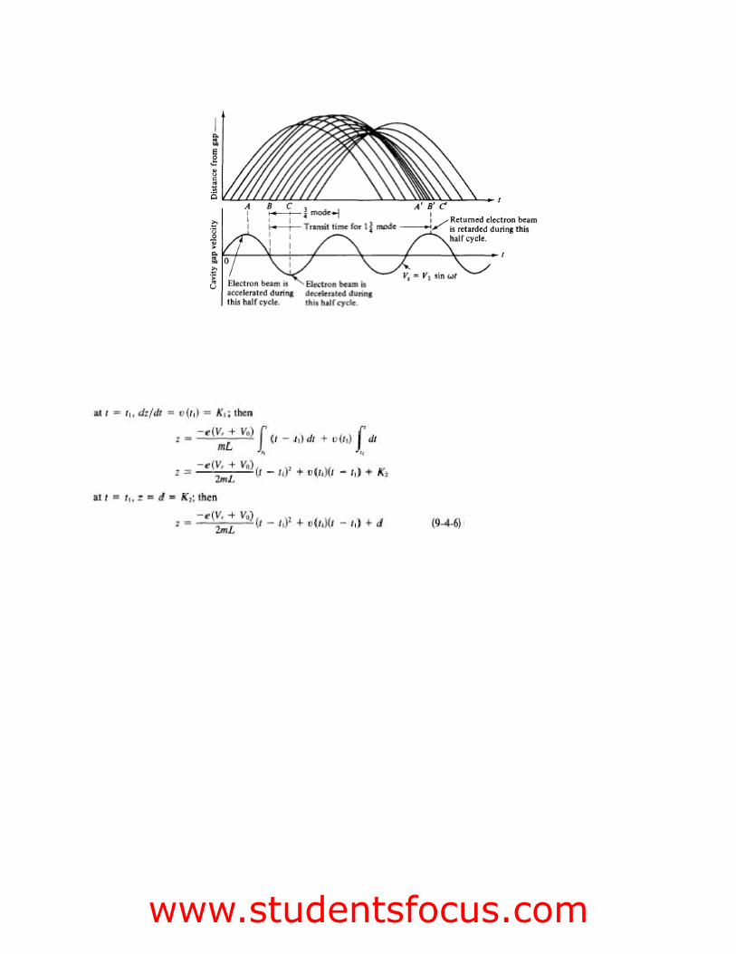
Fatima Michael College of Engineering & Technology
Fatima Michael College of Engineering & Technology
Fatima Michael College of Engineering & Technologywww.studentsfocus.com
5.4 TRAVELING WAVE TUBE
Since Kompfner invented the helix traveling-wave tube (TWT) in 1944 [11], its basic circuit has changed
little. For broadband applications, the helix TWTs are almost exclusively used, whereas for high-average-
power purposes, such as radar transmitters, the coupled-cavity TWTs are commonly used.
In previous sections klystrons and reflex klystrons were analyzed in some detail. Before starting to
describe the TWT, it seems appropriate to compare the basic operating principles of both the TWT and
the klystron. In the case of the TWT, the microwave circuit is nonresonant and the wave propagates with
the same speed as the electrons in the beam. The initial effect on the beam is a small amount of velocity
modulation caused by the weak electric fields associated with the traveling wave.
Just as in the klystron, this velocity modulation later translates to current modulation, which then induces
an RF current in the circuit, causing amplification. However, there are some major differences between
the TWT and the klystron:
Fatima Michael College of Engineering & Technology
Fatima Michael College of Engineering & Technology
Fatima Michael College of Engineering & Technologywww.studentsfocus.com
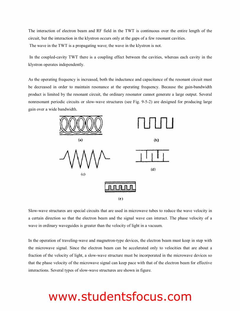
The interaction of electron beam and RF field in the TWT is continuous over the entire length of the
circuit, but the interaction in the klystron occurs only at the gaps of a few resonant cavities.
The wave in the TWT is a propagating wave; the wave in the klystron is not.
In the coupled-cavity TWT there is a coupling effect between the cavities, whereas each cavity in the
klystron operates independently.
As the operating frequency is increased, both the inductance and capacitance of the resonant circuit must
be decreased in order to maintain resonance at the operating frequency. Because the gain-bandwidth
product is limited by the resonant circuit, the ordinary resonator cannot generate a large output. Several
nonresonant periodic circuits or slow-wave structures (see Fig. 9-5-2) are designed for producing large
gain over a wide bandwidth.
Slow-wave structures are special circuits that are used in microwave tubes to reduce the wave velocity in
a certain direction so that the electron beam and the signal wave can interact. The phase velocity of a
wave in ordinary waveguides is greater than the velocity of light in a vacuum.
In the operation of traveling-wave and magnetron-type devices, the electron beam must keep in step with
the microwave signal. Since the electron beam can be accelerated only to velocities that are about a
fraction of the velocity of light, a slow-wave structure must be incorporated in the microwave devices so
that the phase velocity of the microwave signal can keep pace with that of the electron beam for effective
interactions. Several types of slow-wave structures are shown in figure.
Fatima Michael College of Engineering & Technology
Fatima Michael College of Engineering & Technology
Fatima Michael College of Engineering & Technologywww.studentsfocus.com

5.5 MAGNETRON
MAGNETRON OSCILLATORS
Hull invented the magnetron in 1921 [1], but it was only an interesting laboratory device until about 1940.
During World War II, an urgent need for high-power microwave generators for radar transmitters led to
the rapid development of the magnetron to its present state.
All magnetrons consist of some form of anode and cathode operated in a de magnetic field normal to of
the crossed field between the cathode and anode, the electrons emitted from the cathode are influenced by
the crossed field to move in curved paths. If the de magnetic field is strong enough, the electrons will not
arrive in the anode but return instead to the cathode. Consequently, the anode current is cut off.
Magnetrons can be classified into three types:
1. Split-anode magnetron: This type of magnetron uses a static negative resistance between two anode
segments.
2. Cyclotron-frequency magnetrons: This type operates under the influence of synchronism between an
alternating component of electric field and a periodic oscillation of electrons in a direction parallel to the
field.
3. Traveling-wave magnetrons: This type depends on the interaction of electrons with a traveling
electromagnetic field of linear velocity. They are customarily referred to simply as magnetrons.
Cylindrical Magnetron
A schematic diagram of a cylindrical magnetron oscillator is shown in Fig. 10-1-1. This type of
magnetron is also called a conventional magnetron.
In a cylindrical magnetron, several reentrant cavities are connected to the gaps. The de voltage Vo is
applied between the cathode and the anode. The magnetic flux density Bo is in the positive z direction.
When the de voltage and the magnetic flux are adjusted properly, the electrons will follow cycloidal paths
Fatima Michael College of Engineering & Technology
Fatima Michael College of Engineering & Technology
Fatima Michael College of Engineering & Technologywww.studentsfocus.com
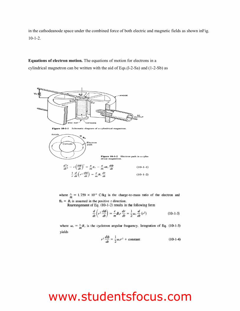
in the cathodeanode space under the combined force of both electric and magnetic fields as shown inFig.
10-1-2.
Equations of electron motion. The equations of motion for electrons in a
cylindrical magnetron can be written with the aid of Eqs.(l-2-Sa) and (1-2-Sb) as
Fatima Michael College of Engineering & Technology
Fatima Michael College of Engineering & Technology
Fatima Michael College of Engineering & Technologywww.studentsfocus.com

Cyclotron angular frequency. Since the magnetic field is normal to the motion of electrons that travel in a cycloidal path, the outward centrifugal force is
equal to the pulling force. Hence
Fatima Michael College of Engineering & Technology
Fatima Michael College of Engineering & Technology
Fatima Michael College of Engineering & Technologywww.studentsfocus.com
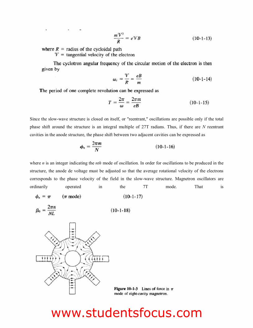
Since the slow-wave structure is closed on itself, or "reentrant," oscillations are possible only if the total
phase shift around the structure is an integral multiple of 27T radians. Thus, if there are N reentrant
cavities in the anode structure, the phase shift between two adjacent cavities can be expressed as
where n is an integer indicating the nth mode of oscillation. In order for oscillations to be produced in the
structure, the anode de voltage must be adjusted so that the average rotational velocity of the electrons
corresponds to the phase velocity of the field in the slow-wave structure. Magnetron oscillators are
ordinarily operated in the 7T mode. That is
Fatima Michael College of Engineering & Technology
Fatima Michael College of Engineering & Technology
Fatima Michael College of Engineering & Technologywww.studentsfocus.com

Maxwell's equations subject to the boundary conditions. The solution for the fundamental cf> component
of the electric field has the form [l]
where £ 1 is a constant and f3o is given in Eq. (10-1-18). Thus, the traveling field of the fundamental
mode travels around the structure with angular velocity
where~ can be found from Eq. (10-1-19). When the cyclotron frequency of the electrons is equal to the
angular frequency of the field, the interactions between the field and electron occurs and the energy is
transferred. That is,
5.6 MEASUREMENT OF POWER
Power Measurement 9 Power is defined as the quantity of energy dissipated or stored per unit time.
9 Microwave power is divided into three categories – low power (less than 10mW), medium power
(from 10mW to 10W) and high power (greater than 10w).
9 The general measurement technique for average power is to attach a properly calibrated sensor to
the transmission line port at which the unknown power is to be measured.
9 The output from the sensor is connected to an appropriate power meter. The RF power to the
sensor is turned off and the power meter zeroed. This operation is often referred to as “zero
setting” or “zeroing.” Power is then turned on.
9 The sensor, reacting to the new input level, sends a signal to the power meter and the new meter
reading is observed.
9 There are three popular devices for sensing and measuring average power at RF and microwave
frequencies. Each of the methods uses a different kind of device to convert the RF power to a
measurable DC or low frequency signal. The devices are the diode detector, the bolometer and
the thermocouple.
Fatima Michael College of Engineering & Technology
Fatima Michael College of Engineering & Technology
Fatima Michael College of Engineering & Technologywww.studentsfocus.com
Diode Detector
The low-barrier Schottky (LBS) diode technology which made it possible to construct diodes with metal-
semiconductor junctions for microwave frequencies that was very rugged and consistent from diode to
diode. These diodes, introduced as power sensors in 1974, were able to detect and measure power as low
as −70 dBm (100 pW) at frequencies up to 18 GHz.
Bolometer Sensor:
Bolometers are power sensors that operate by changing resistance due to a change in temperature. The
change in temperature results from converting RF or microwave energy into heat within the bolometric
element. There are two principle types of bolometers, barretters and thermistors. A barretter is a thin wire
that has a positive temperature coefficient of resistance. Thermistors are semiconductors with a negative
temperature coefficient.
Thermistor elements are mounted in either coaxial or waveguide structures so they are compatible with
common transmission line systems used at microwave and RF frequencies.
Power meters are constructed from balanced bridge circuits. The principal parts of the power meter are
two self-balancing bridges, the meter-logic section, and the auto-zero circuit. The RF Bridge, which
contains the detecting thermistor, is kept in balance by automatically varying the DC voltage Vrf, which
drives that bridge. The compensating bridge, which contains the compensating thermistor, is kept in
balance by automatically varying the DC voltage Vc, which drives that bridge. The power meter is
initially zero-set (by pushing the zero-set button) with no applied RF power by making Vc equal to Vrfo
(Vrfo means Vrf with zero RF power). After zero-setting, if ambient temperature variations change
thermistor resistance, both bridge circuits respond by applying the same new voltage to maintain balance.
If RF power is applied to the detecting thermistor, Vrf decreases so that
Where Prf is the RF power applied and R is the value of the thermistor resistance at balance. But from
zero-setting, Vrfo= Vc so that
Fatima Michael College of Engineering & Technology
Fatima Michael College of Engineering & Technology
Fatima Michael College of Engineering & Technologywww.studentsfocus.com
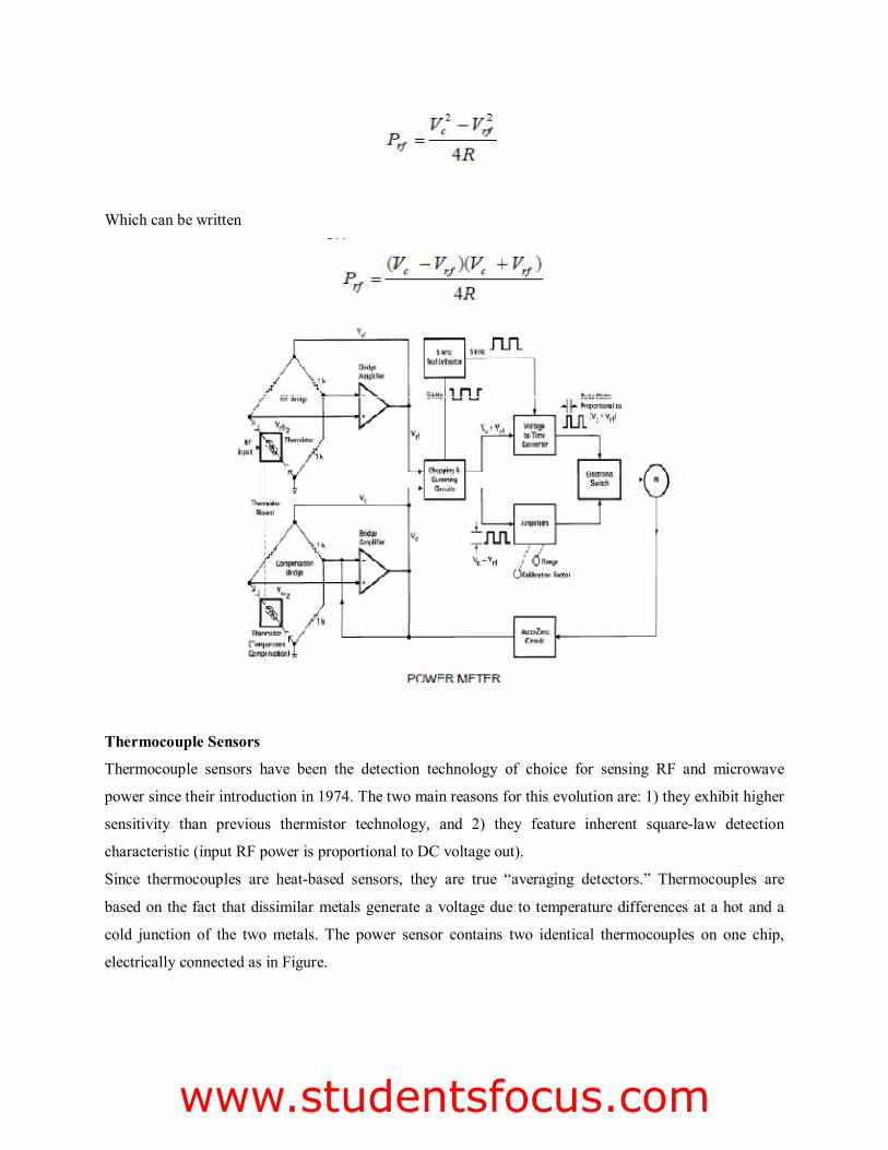
Which can be written
Thermocouple Sensors
Thermocouple sensors have been the detection technology of choice for sensing RF and microwave
power since their introduction in 1974. The two main reasons for this evolution are: 1) they exhibit higher
sensitivity than previous thermistor technology, and 2) they feature inherent square-law detection
characteristic (input RF power is proportional to DC voltage out).
Since thermocouples are heat-based sensors, they are true “averaging detectors.” Thermocouples are
based on the fact that dissimilar metals generate a voltage due to temperature differences at a hot and a
cold junction of the two metals. The power sensor contains two identical thermocouples on one chip,
electrically connected as in Figure.
Fatima Michael College of Engineering & Technology
Fatima Michael College of Engineering & Technology
Fatima Michael College of Engineering & Technologywww.studentsfocus.com
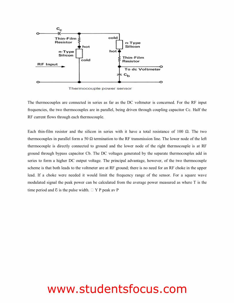
The thermocouples are connected in series as far as the DC voltmeter is concerned. For the RF input
frequencies, the two thermocouples are in parallel, being driven through coupling capacitor Cc. Half the
RF current flows through each thermocouple.
Each thin-film resistor and the silicon in series with it have a total resistance of 100 Ω. The two
thermocouples in parallel form a 50 Ω termination to the RF transmission line. The lower node of the left
thermocouple is directly connected to ground and the lower node of the right thermocouple is at RF
ground through bypass capacitor Cb. The DC voltages generated by the separate thermocouples add in
series to form a higher DC output voltage. The principal advantage, however, of the two thermocouple
scheme is that both leads to the voltmeter are at RF ground; there is no need for an RF choke in the upper
lead. If a choke were needed it would limit the frequency range of the sensor. For a square wave
modulated signal the peak power can be calculated from the average power measured as where T is the
time period and Շ is the pulse width. Y P peak av P
Fatima Michael College of Engineering & Technology
Fatima Michael College of Engineering & Technology
Fatima Michael College of Engineering & Technologywww.studentsfocus.com
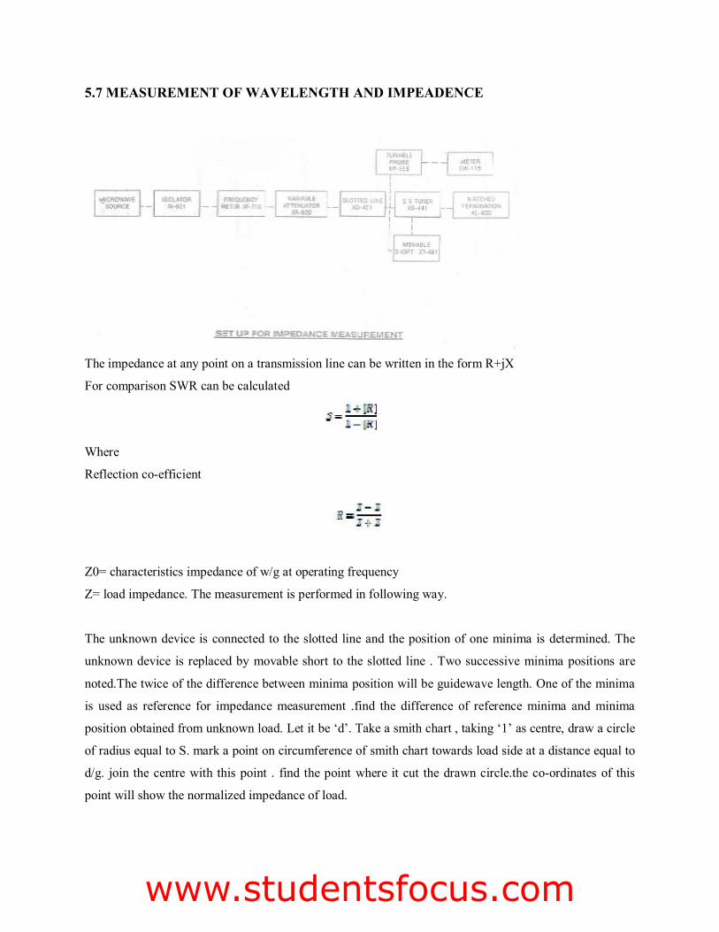
5.7 MEASUREMENT OF WAVELENGTH AND IMPEADENCE
The impedance at any point on a transmission line can be written in the form R+jX
For comparison SWR can be calculated
Where
Reflection co-efficient
Z0= characteristics impedance of w/g at operating frequency
Z= load impedance. The measurement is performed in following way.
The unknown device is connected to the slotted line and the position of one minima is determined. The
unknown device is replaced by movable short to the slotted line . Two successive minima positions are
noted.The twice of the difference between minima position will be guidewave length. One of the minima
is used as reference for impedance measurement .find the difference of reference minima and minima
position obtained from unknown load. Let it be ‘d’. Take a smith chart , taking ‘1’ as centre, draw a circle
of radius equal to S. mark a point on circumference of smith chart towards load side at a distance equal to
d/g. join the centre with this point . find the point where it cut the drawn circle.the co-ordinates of this
point will show the normalized impedance of load.
Fatima Michael College of Engineering & Technology
Fatima Michael College of Engineering & Technology
Fatima Michael College of Engineering & Technologywww.studentsfocus.com

PROCEDURE:
1.Setup the components and equipments as shown in figure.
2. Setup variable attenuator at minimum attenuation position.
3. Keep the control knobs of VSWR meter as below:
Range - 50db position
Input switch - Crystal low impedance
Meter switch - Normal position
Gain(Coarse & Fine)- Mid position
4. Keep the control knobs of Klystron power supply as below
Beam voltage - ‘OFF’
Mod-switch -AM
Beam Voltage knob-Fully anticlockwise
Reflector Voltage- Fully clockwise
AM- Amplitude knob- Around fully clockwise
AM- Frequency knob – Around Mid position
5. Switch ‘ON’ the Klystron power supply, VSWR Meter and cooling fan switch.
6. Switch ‘ON’ the beam voltage switch and set beam voltage around 250V-300V with help of beam
voltage knob.
7. Adjust the reflector voltage to get some deflection in VSWR meter.
8. Maximize the deflection with AM amplitude and frequency control knob of power supply.
9. Tune the plunger of Klystron Mount for maximum deflection.
10. Tune the reflector voltage knob for maximum deflection .
11. Tune the probe for maximum deflection in VSWR Meter.
12. Tune the frequency meter knob to get a ‘dip’ on the VSWR scale and note down the frequency
directly from frequency meter.
13. Keep the depth of pin S S. Tuner to around 3-4 mm and lock it.
14. Move the probe along the slotted line to get maximum deflection.
15. Adjust VSWR meter gain control knob and variable attenuator until the meter indicates
1.0 on the normal db SWR scale.
16. Move the probe to next minimum position and note down the SWR S0 on the scale .also note down
the probe position. Let it be ‘d’.
17. Remove the SS tuner and matched termination and place movable short at slotted line. The plunger of
short should be at zero.
18. Note the position of two successive minima position .let it be as d1 and d2 .Hence λg = 2(d1- d2).
Fatima Michael College of Engineering & Technology
Fatima Michael College of Engineering & Technology
Fatima Michael College of Engineering & Technologywww.studentsfocus.com
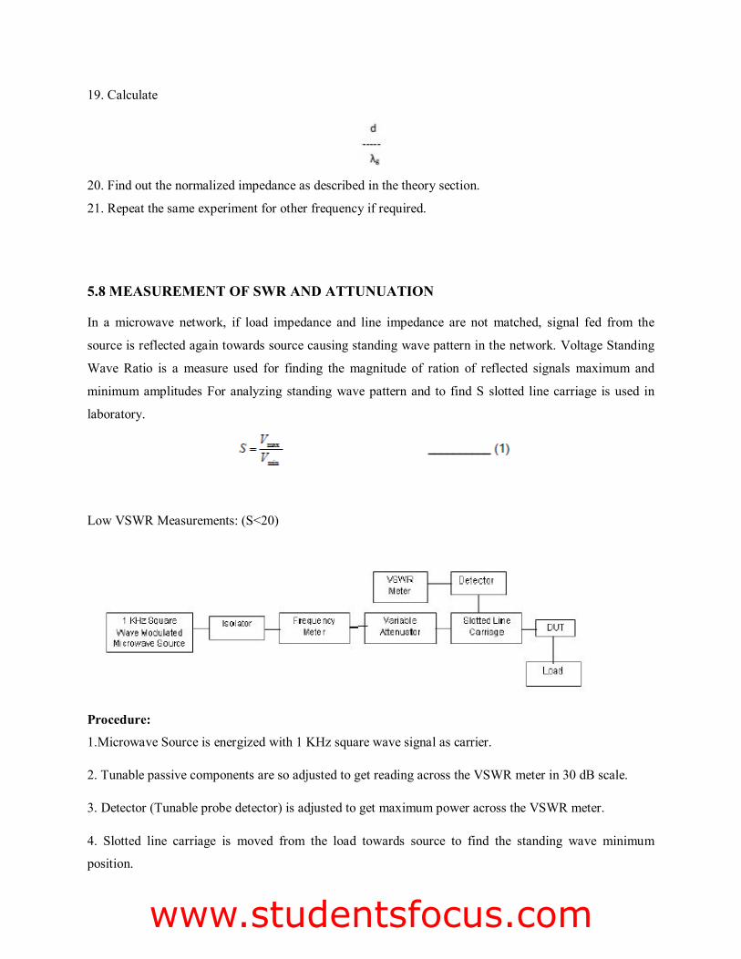
19. Calculate
20. Find out the normalized impedance as described in the theory section.
21. Repeat the same experiment for other frequency if required.
5.8 MEASUREMENT OF SWR AND ATTUNUATION
In a microwave network, if load impedance and line impedance are not matched, signal fed from the
source is reflected again towards source causing standing wave pattern in the network. Voltage Standing
Wave Ratio is a measure used for finding the magnitude of ration of reflected signals maximum and
minimum amplitudes For analyzing standing wave pattern and to find S slotted line carriage is used in
laboratory.
Low VSWR Measurements: (S<20)
Procedure:
1.Microwave Source is energized with 1 KHz square wave signal as carrier.
2. Tunable passive components are so adjusted to get reading across the VSWR meter in 30 dB scale.
3. Detector (Tunable probe detector) is adjusted to get maximum power across the VSWR meter.
4. Slotted line carriage is moved from the load towards source to find the standing wave minimum
position.
Fatima Michael College of Engineering & Technology
Fatima Michael College of Engineering & Technology
Fatima Michael College of Engineering & Technologywww.studentsfocus.com

5. By adjusting the gain control knob of VSWR meter and attenuator the reading across the VSWR meter
is made as 1 or 0 dB known as normalization.
6. Again the slotted carriage is moved towards source to find the next minimum position. The reading
shown at this point in the VSWR meter is the ratio of magnitude of reflected signals minimum and
maximum voltages ( ). min max VV S
7. VSWR meter has three different scales with different ranges as specified below.
a) NORMAL SWR Scale 1 ---- 1 – 4
b) NORMAL SWR Scale 2 ---- 3.2 – 10
c) EXPANDED SWR Scale 3 ---- 1 – 1.33
8. If the device under test (DUT) is having the range of VSWR 1 – 4, reading is taken from the first scale
from the top (NORMAL SWR Scale 1 – 1 – 4).
9. If the device under test (DUT) is having the range of VSWR 3.2 – 10, reading is taken from the second
scale from the top (NORMAL SWR Scale 2 (3.2 – 10).
10. If the device under test (DUT) is having the range of VSWR 1 – 1.33, reading is taken from the third
scale from the top (EXPANDED SWR Scale 3 (1 – 1.33).
11. If the device under test (DUT) is having the range of VSWR 10 – 40, a 20 dB range is selected in the
VSWR meter and reading is taken from the first scale from the top (NORMAL SWR Scale 1 – 1 – 4)
which is then multiplied by 10 for getting the actual reading.
Possible Errors in Measurements:
1. Detector may not work square law region for both Vmax. and Vmin.
2. Depth of the probe in the slotted line carriage is made as minimum. If not, it may cause reflections in
addition to the load reflections.
3. For the device having low VSWR, connector used for measurement must have proper matching with
line impedance.
4. If the geometrical shape of the slotted line is not proper, Vmax. (or) Vmin. Value will not constant
across the slotted line.
Fatima Michael College of Engineering & Technology
Fatima Michael College of Engineering & Technology
Fatima Michael College of Engineering & Technologywww.studentsfocus.com
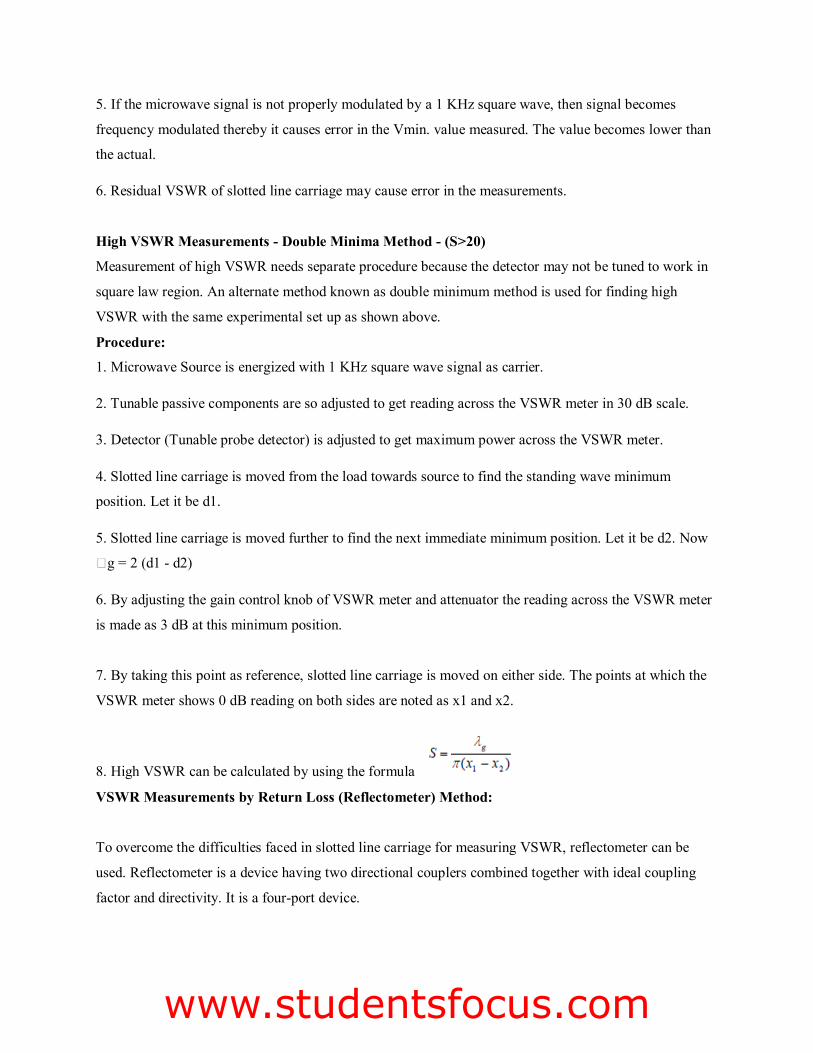
5. If the microwave signal is not properly modulated by a 1 KHz square wave, then signal becomes
frequency modulated thereby it causes error in the Vmin. value measured. The value becomes lower than
the actual.
6. Residual VSWR of slotted line carriage may cause error in the measurements.
High VSWR Measurements - Double Minima Method - (S>20)
Measurement of high VSWR needs separate procedure because the detector may not be tuned to work in
square law region. An alternate method known as double minimum method is used for finding high
VSWR with the same experimental set up as shown above.
Procedure:
1. Microwave Source is energized with 1 KHz square wave signal as carrier.
2. Tunable passive components are so adjusted to get reading across the VSWR meter in 30 dB scale.
3. Detector (Tunable probe detector) is adjusted to get maximum power across the VSWR meter.
4. Slotted line carriage is moved from the load towards source to find the standing wave minimum
position. Let it be d1.
5. Slotted line carriage is moved further to find the next immediate minimum position. Let it be d2. Now
g = 2 (d1 - d2)
6. By adjusting the gain control knob of VSWR meter and attenuator the reading across the VSWR meter
is made as 3 dB at this minimum position.
7. By taking this point as reference, slotted line carriage is moved on either side. The points at which the
VSWR meter shows 0 dB reading on both sides are noted as x1 and x2.
8. High VSWR can be calculated by using the formula
VSWR Measurements by Return Loss (Reflectometer) Method:
To overcome the difficulties faced in slotted line carriage for measuring VSWR, reflectometer can be
used. Reflectometer is a device having two directional couplers combined together with ideal coupling
factor and directivity. It is a four-port device.
Fatima Michael College of Engineering & Technology
Fatima Michael College of Engineering & Technology
Fatima Michael College of Engineering & Technologywww.studentsfocus.com

Experimental Procedure:
1. Microwave Source is energized with 1 KHz square wave signal as carrier.
2. Tunable passive components are so adjusted to get reading across the VSWR meter in 30 dB scale.
3. Detector (Tunable probe detector) is adjusted to get maximum power across the VSWR meter.
4. Port 2 is with a movable short and is adjusted for getting the output across the detector to unity in
VSWR meter. Port 3 is matched terminated.
5. VSWR meter and matched load at port4 and port 3 are interchanged. The output of the port3 is noted
which should be ideally equal to the output from port 4.
6. Without disturbing the VSWR meter adjustment, the unknown load is connected at port 2 byreplacing
the short and the output at port3 is noted to obtain
directly from the VSWR meter.
Return loss =
This method is well suited for loads having low VSWR. The major sources of errors are
1. Unstability of the signal source causes a change of signal power level during measurement of input and
reflected signals.
2. Non-ideal directional couplers and detectors are also sources of error.
Fatima Michael College of Engineering & Technology
Fatima Michael College of Engineering & Technology
Fatima Michael College of Engineering & Technologywww.studentsfocus.com

5.9 Q AND PHASE SHIFT
Microwave frequency can be measured by a number of different mechanical and electronic techniques.
9 Mechanical techniques
9 Slotted Line Method (Indirect Method)
The standing waves setup in a transmission line or a waveguide produce minima every half wavelength
apart.
These minima are detected and the distance between them is measured. From which the wavelength and
frequency can be calculated by
Resonant Cavity Method (Direct Method)
The most commonly used type of microwave frequency meter is wave meters. It consists of a cylindrical
or coaxial resonant cavity. The size of the cavity can be altered by adjustable plunger. The cavity is
Fatima Michael College of Engineering & Technology
Fatima Michael College of Engineering & Technology
Fatima Michael College of Engineering & Technologywww.studentsfocus.com
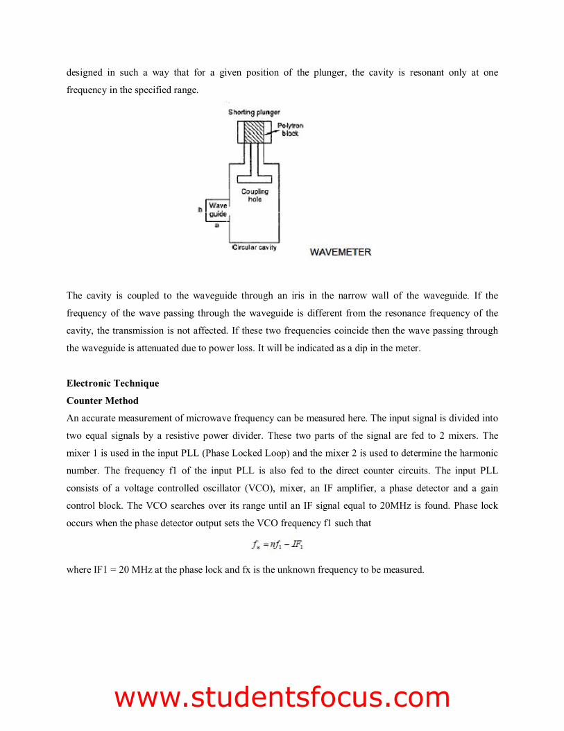
designed in such a way that for a given position of the plunger, the cavity is resonant only at one
frequency in the specified range.
The cavity is coupled to the waveguide through an iris in the narrow wall of the waveguide. If the
frequency of the wave passing through the waveguide is different from the resonance frequency of the
cavity, the transmission is not affected. If these two frequencies coincide then the wave passing through
the waveguide is attenuated due to power loss. It will be indicated as a dip in the meter.
Electronic Technique
Counter Method
An accurate measurement of microwave frequency can be measured here. The input signal is divided into
two equal signals by a resistive power divider. These two parts of the signal are fed to 2 mixers. The
mixer 1 is used in the input PLL (Phase Locked Loop) and the mixer 2 is used to determine the harmonic
number. The frequency f1 of the input PLL is also fed to the direct counter circuits. The input PLL
consists of a voltage controlled oscillator (VCO), mixer, an IF amplifier, a phase detector and a gain
control block. The VCO searches over its range until an IF signal equal to 20MHz is found. Phase lock
occurs when the phase detector output sets the VCO frequency f1 such that
where IF1 = 20 MHz at the phase lock and fx is the unknown frequency to be measured.
Fatima Michael College of Engineering & Technology
Fatima Michael College of Engineering & Technology
Fatima Michael College of Engineering & Technologywww.studentsfocus.com
The f1 is translated to a frequency f2 so that
where f0 = 20 MHz offset frequency. This is done by a frequency translation unit (FTU). The frequency
f2 drives the second sampler and produces a second output. IF2 is given as
By mixing IF2 with IF1 and rejecting 20 MHz and higher frequencies, nf0 is obtained. Counting the
number of zero crossing for the period of f0, determines the harmonic number n of the phase lock loop.
The input frequency is then calculated by presetting into IFref counter, measuring f1 and extending gate
time according to number n.
Fatima Michael College of Engineering & Technology
Fatima Michael College of Engineering & Technology
Fatima Michael College of Engineering & Technologywww.studentsfocus.com


![[ V ] r ( ) rf + Ñ × rf - GÑf t - fem.unicamp.brphoenics/SITE_PHOENICS/AULAS/ENERGY_EQ… · rf + Ñ × rf - GÑf = ... Novas variáveis podem ser introduzidas via VR ou diretamente](https://static.fdocument.org/doc/165x107/5ba2a4ee09d3f2d14d8c57c4/-v-r-rf-n-rf-gnf-t-fem-phoenicssitephoenicsaulasenergyeq.jpg)


![The modern port of patras el[1]](https://static.fdocument.org/doc/165x107/557ea112d8b42ac5658b47de/the-modern-port-of-patras-el1.jpg)