REF Control Logics NSA2200: General Sensor Conditioner ...€¦ · NSA2200: General Sensor...
21
NOVOSENSE NSA2200: General Sensor Conditioner with Digital Temperature Calibration Datasheet Product Overview The NSA2200 is a highly integrated, low power high precision sensor conditioner for general resistive bridge sensors, which features a low noise instrument amplifier, a low power 24 bit Σ-Δ ADC, a digital sensor calibration DSP. The NSA2200 can provide an on-chip digital compensation of sensor offset, gain, temperature drift and non-linearity based on the internal fuse banks (OTP), which is fast, precise, without the cost overhead with trimming by laser or external components. Multiple temperature sensing methods are supported by NSA2200 for sensor’s temperature calibrating. I2C and SPI interfaces are supported for chip configuration, sensor calibrating and digital output. Key Features Input referred RMS noise: 600nV @ OSR=1024X, GAIN=32X OTP based digital calibration of sensor offset, sensitivity, temperature drift and non-linearity with a calibration precision up to 0.05% full scale. 1X~128X programmable gain for sensors with different input spans up to rail-to-rail. Full set of diagnostic features Low power instrument amplifier and 24-bit Σ-Δ ADC Multiple temperature sensing methods 8-level resolution settings for conversion time and accuracy trade off SPI / I2C serial interface Ultra low power-down current ( < 0.2uA@25℃ ) Supply voltage 1.8V to 5.5V Operation temperature from -40°C to 125°C Available Supports Evaluation kit with calibration procedure for fast user design Support for mass calibration Quick circuit customization possible Applications Pressure sensor conditioner Magnetic sensor conditioner Strain Gauge interface Industry process control VDD SDA/SDI/SDIO SDO/ADRESS VDDIO OSC &Timing ADC REF Filter& DSP Serial Interface SCL CSB INT PGA POR Buffer VINP PSW TEMP VINN Control Logics OTP GND Temp_offset 4X~64X VDD Int Temp sensor Diag VEXT MUX
Transcript of REF Control Logics NSA2200: General Sensor Conditioner ...€¦ · NSA2200: General Sensor...
NOVOSENSE
NSA2200: General Sensor Conditioner with Digital Temperature Calibration
Datasheet
Product Overview
The NSA2200 is a highly integrated, low power
high precision sensor conditioner for general
resistive bridge sensors, which features a low
noise instrument amplifier, a low power 24 bit Σ-Δ
ADC, a digital sensor calibration DSP. The
NSA2200 can provide an on-chip digital
compensation of sensor offset, gain, temperature
drift and non-linearity based on the internal fuse
banks (OTP), which is fast, precise, without the
cost overhead with trimming by laser or external
components. Multiple temperature sensing
methods are supported by NSA2200 for sensor’s
temperature calibrating. I2C and SPI interfaces are
supported for chip configuration, sensor
calibrating and digital output.
Key Features
Input referred RMS noise: 600nV @
OSR=1024X, GAIN=32X
OTP based digital calibration of sensor offset,
sensitivity, temperature drift and non-linearity
with a calibration precision up to 0.05% full
scale.
1X~128X programmable gain for sensors with
different input spans up to rail-to-rail.
Full set of diagnostic features
Low power instrument amplifier and 24-bit Σ-Δ
ADC
Multiple temperature sensing methods
8-level resolution settings for conversion time
and accuracy trade off
SPI / I2C serial interface
Ultra low power-down current ( < 0.2uA@25℃ )
Supply voltage 1.8V to 5.5V
Operation temperature from -40°C to 125°C
Available Supports
Evaluation kit with calibration procedure for fast
user design
Support for mass calibration
Quick circuit customization possible
Applications
Pressure sensor conditioner
Magnetic sensor conditioner
Strain Gauge interface
Industry process control
VDD
SDA/SDI/SDIO
SDO/ADRESS
VDDIO
OSC &Timing
ADC
REF
Filter&
DSP
Serial
InterfaceSCL
CSB
INT
PGA
POR
Buffer
VINP
PSW
TEMP
VINN
Control Logics
OTP
GND
Temp_offset
4X~64X
VDD
Int Temp
sensor
Diag
VEXT
MUX
NSA2200
Novosense Confidential Page 2
1.0 ABSOLUTE MAXIMUM RATING ................................................................................................................................. 3
2.0 ELECTRICAL CHARACTERISITICS .......................................................................................................................... 3
3.0 REGISTERS ....................................................................................................................................................................... 4
3.1. NORMAL REGISTERS ...................................................................................................................................................... 4 3.2. OTP REGISTERS ................................................................................................................................................................ 5
4.0 FUNCTIONAL DESCRIPTIONS .................................................................................................................................... 6
4.1. SIGNAL PATH ..................................................................................................................................................................... 7 4.1.1. Analog Inputs and Reference .................................................................................................................................... 7 4.1.2. PGA, Buffer and Modulator...................................................................................................................................... 7 4.1.3. Digital Filter with Programmable Over-Sampling Factor ....................................................................................... 7 4.1.4. Work Mode ................................................................................................................................................................ 8 4.1.4.1. Single-shot Sensor Signal Conversion .................................................................................................................. 8 4.1.4.2. Single-shot Temperature Conversion .................................................................................................................... 8 4.1.4.3. Combined conversion .......................................................................................................................................... 10 4.1.4.4. Sleep conversion ................................................................................................................................................. 10 4.1.4.5. Diagnostic features ............................................................................................................................................. 11
4.2. OTP ................................................................................................................................................................................ 11 4.3. SENSOR CALIBRATION .................................................................................................................................................... 12
5.0 SPI INTERFACE ............................................................................................................................................................. 12
5.1. INTERFACE SPECIFICATION .............................................................................................................................................. 12
6.0 I2C INTERFACE ............................................................................................................................................................. 14
7.0 PAD ASSIGNMENT ........................................................................................................................................................ 15
8.0 TYPICAL APPLICATION ............................................................................................................................................. 19
8.1. I2C MODE FOR BARE DIE ................................................................................................................................................ 19 8.2. SPI MODE FOR BARE DIE ................................................................................................................................................. 20 8.3. I2C MODE FOR SOP-8 PACKAGED CHIP ........................................................................................................................... 20
9.0 ORDER INFORMATION ............................................................................................................................................... 20
10.0 DOCUMENT HISTORY AND MODIFICATION ........................................................................................................ 21
NSA2200
Novosense Confidential Page 3
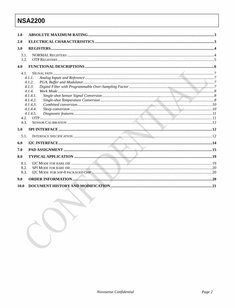
1.0 ABSOLUTE MAXIMUM RATING
Parameter Symbol Min Typ Max Unit Comments
Supply Voltage VDD -0.3 6.5 V
VDDIO -0.3 6.5 V
Analog pin voltage -0.3 VDD+0.3 V
Digital output voltage -0;3 VDDIO+0.3 V 25°C
ESD Susceptibility 4 kV HBM
Storage temperature -60 150 °C
2.0 ELECTRICAL CHARACTERISITICS
Parameter Symbol Min Typ Max Unit Comments
Supply/Regulation
Supply Voltage VDD 1.8 5.5 V
VDDIO 1.2V 5.5 V
Operation temp TBAB -40 125 °C
Supply Current@25°C
on during conversion
IBDD_pgaoffB 900 uA PGA off (Gain<=2)
IBDD_pgaonB 1500 uA PGA on (Gain>=4)
Idd_dac 1700 uA PGA on
Standby current IBsdB 100 nA 25°C
Regulator PSRR 60 dB
Current load on
Regulator
Iload 5mA
Signal Chain (MUX+PGA+BUFFER+ADC) CHARACTERISTICS
Resolution N 24 Bits
Conversation time Tcnv Depend on OSR setting, refer
to Table 4.1
Ms
Output Data Resolution 24 Bit LSB = (1/2^23)*(VEXT-PSW)
(‘raw_data_on’=1)
Effective Resolution ENOB refer to Table 4.1 Bits Depends on Gain & OSR
Gain setting GAIN 1 128
Integral Nonlinearity INL 15 ppm of
FS
Input Common Mode CMRR 80 110 dB
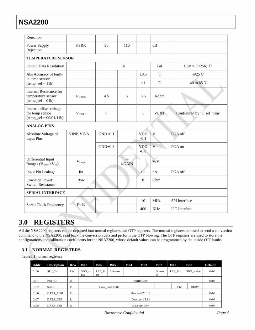
NSA2200
Novosense Confidential Page 4
Rejection
Power Supply
Rejection
PSRR 90 110 dB
TEMPERATURE SENSOR
Output Data Resolution 16 Bit LSB = (1/256) ℃
Abs Accuracy of built-
in temp sensor
(temp_sel = 11b)
±0.5 ℃ @25℃
±1 ℃ -40 to 85 ℃
Internal Resistance for
temperature sensor
(temp_sel = 01b)
RBT-RESB 4.5 5 5.5 Kohm
Internal offset voltage
for temp sensor
(temp_sel = 00/01/11b)
VBT-OFFB 0 1 VEXT Configured by ‘T_ref_trim’
ANALOG PINS
Absolute Voltage of
Input Pins
VINP, VINN GND+0.1 VDD
-0.1
V PGA off
GND+0.4 VDD
-0.8
V PGA on
Differential Input
Ranges (VBoffsetB+VBspB) VBrangeB
+-
1/GAIN V/V
Input Pin Leakage Iin +-1 nA PGA off
Low-side Power
Switch Resistance
Rsw 8 Ohm
SERIAL INTERFACE
Serial Clock Frequency Fsclk 10 MHz SPI Interface
400 KHz I2C Interface
3.0 REGISTERS All the NSA2200 registers can be departed into normal registers and OTP registers. The normal registers are used to send a conversion
command to the NSA2200, read back the conversion data and perform the OTP blowing. The OTP registers are used to store the
configurations and calibration coefficients for the NSA2200, whose default values can be programmed by the inside OTP banks.
3.1. NORMAL REGISTERS
Table3.1 normal registers
Addr Description R/W Bit7 Bit6 Bit5 Bit4 Bit3 Bit2 Bit1 Bit0 Default
0x00 SPI _Ctrl RW SDO_ac
tive
LSB_fi
rst
Softreset Softres
et
LSB_first SDO_active 0x00
0x01 Part_ID R PartID<7:0> 0x00
0x02 Status R Error_code<3:0> 1’b0 DRDY
0x06 DATA_MSB R Data out<23:16> 0x00
0x07 DATA_CSB R Data out<15:8> 0x00
0x08 DATA_LSB R Data out<7:0> 0x00
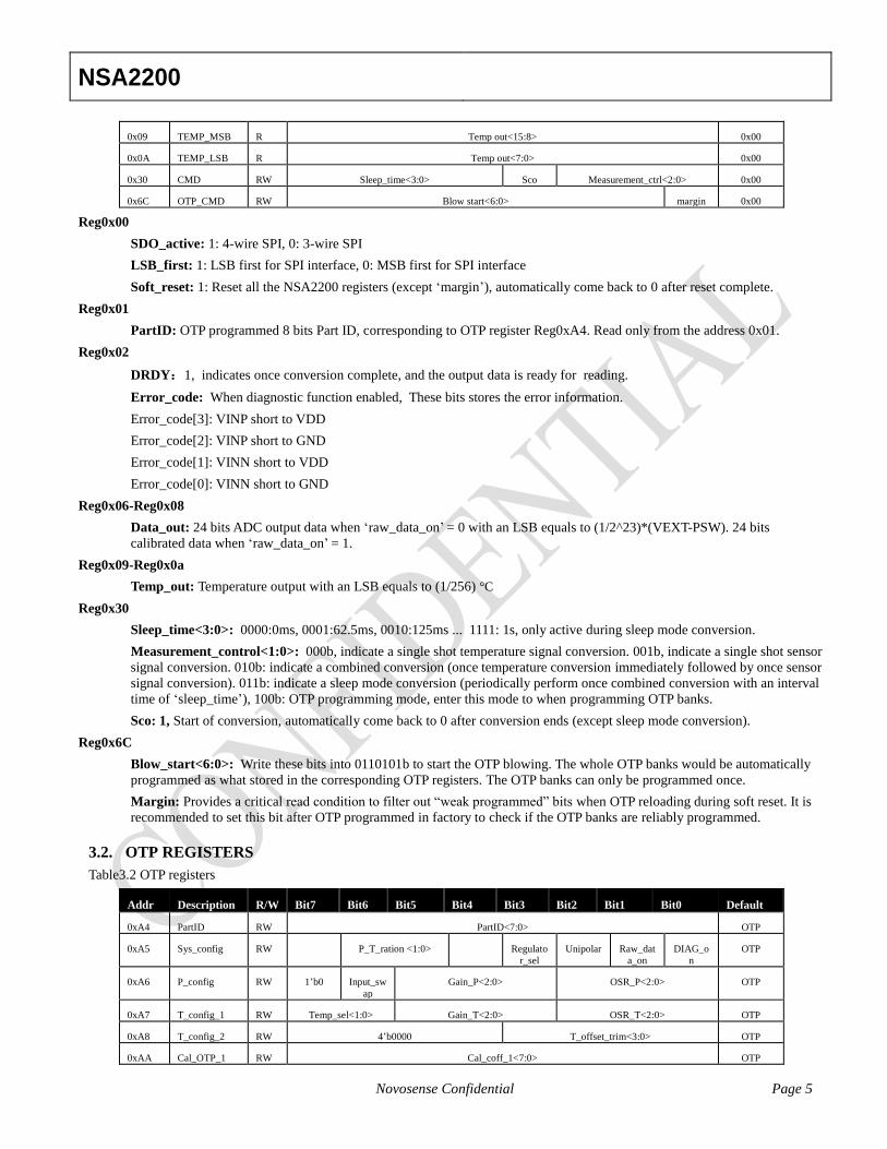
NSA2200
Novosense Confidential Page 5
0x09 TEMP_MSB R Temp out<15:8> 0x00
0x0A TEMP_LSB R Temp out<7:0> 0x00
0x30 CMD RW Sleep_time<3:0> Sco Measurement_ctrl<2:0> 0x00
0x6C OTP_CMD RW Blow start<6:0> margin 0x00
Reg0x00
SDO_active: 1: 4-wire SPI, 0: 3-wire SPI
LSB_first: 1: LSB first for SPI interface, 0: MSB first for SPI interface
Soft_reset: 1: Reset all the NSA2200 registers (except ‘margin’), automatically come back to 0 after reset complete.
Reg0x01
PartID: OTP programmed 8 bits Part ID, corresponding to OTP register Reg0xA4. Read only from the address 0x01.
Reg0x02
DRDY:1, indicates once conversion complete, and the output data is ready for reading.
Error_code: When diagnostic function enabled, These bits stores the error information.
Error_code[3]: VINP short to VDD
Error_code[2]: VINP short to GND
Error_code[1]: VINN short to VDD
Error_code[0]: VINN short to GND
Reg0x06-Reg0x08
Data_out: 24 bits ADC output data when ‘raw_data_on’ = 0 with an LSB equals to (1/2^23)*(VEXT-PSW). 24 bits
calibrated data when ‘raw_data_on’ = 1.
Reg0x09-Reg0x0a
Temp_out: Temperature output with an LSB equals to (1/256) °C
Reg0x30
Sleep_time<3:0>: 0000:0ms, 0001:62.5ms, 0010:125ms ... 1111: 1s, only active during sleep mode conversion.
Measurement_control<1:0>: 000b, indicate a single shot temperature signal conversion. 001b, indicate a single shot sensor
signal conversion. 010b: indicate a combined conversion (once temperature conversion immediately followed by once sensor
signal conversion). 011b: indicate a sleep mode conversion (periodically perform once combined conversion with an interval
time of ‘sleep_time’), 100b: OTP programming mode, enter this mode to when programming OTP banks.
Sco: 1, Start of conversion, automatically come back to 0 after conversion ends (except sleep mode conversion).
Reg0x6C
Blow_start<6:0>: Write these bits into 0110101b to start the OTP blowing. The whole OTP banks would be automatically
programmed as what stored in the corresponding OTP registers. The OTP banks can only be programmed once.
Margin: Provides a critical read condition to filter out “weak programmed” bits when OTP reloading during soft reset. It is
recommended to set this bit after OTP programmed in factory to check if the OTP banks are reliably programmed.
3.2. OTP REGISTERS
Table3.2 OTP registers
Addr Description R/W Bit7 Bit6 Bit5 Bit4 Bit3 Bit2 Bit1 Bit0 Default
0xA4 PartID RW PartID<7:0> OTP
0xA5 Sys_config RW P_T_ration <1:0> Regulato
r_sel
Unipolar Raw_dat
a_on
DIAG_o
n
OTP
0xA6 P_config RW 1’b0 Input_sw
ap
Gain_P<2:0> OSR_P<2:0> OTP
0xA7 T_config_1 RW Temp_sel<1:0> Gain_T<2:0> OSR_T<2:0> OTP
0xA8 T_config_2 RW 4’b0000 T_offset_trim<3:0> OTP
0xAA Cal_OTP_1 RW Cal_coff_1<7:0> OTP
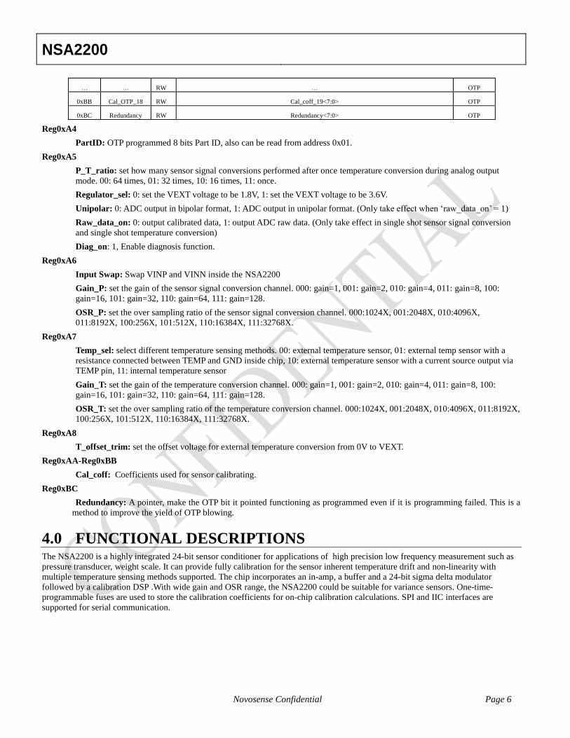
NSA2200
Novosense Confidential Page 6
… … RW … OTP
0xBB Cal_OTP_18 RW Cal_coff_19<7:0> OTP
0xBC Redundancy RW Redundancy<7:0> OTP
Reg0xA4
PartID: OTP programmed 8 bits Part ID, also can be read from address 0x01.
Reg0xA5
P_T_ratio: set how many sensor signal conversions performed after once temperature conversion during analog output
mode. 00: 64 times, 01: 32 times, 10: 16 times, 11: once.
Regulator_sel: 0: set the VEXT voltage to be 1.8V, 1: set the VEXT voltage to be 3.6V.
Unipolar: 0: ADC output in bipolar format, 1: ADC output in unipolar format. (Only take effect when ‘raw_data_on’ = 1)
Raw_data_on: 0: output calibrated data, 1: output ADC raw data. (Only take effect in single shot sensor signal conversion
and single shot temperature conversion)
Diag_on: 1, Enable diagnosis function.
Reg0xA6
Input Swap: Swap VINP and VINN inside the NSA2200
Gain_P: set the gain of the sensor signal conversion channel. 000: gain=1, 001: gain=2, 010: gain=4, 011: gain=8, 100:
gain=16, 101: gain=32, 110: gain=64, 111: gain=128.
OSR_P: set the over sampling ratio of the sensor signal conversion channel. 000:1024X, 001:2048X, 010:4096X,
011:8192X, 100:256X, 101:512X, 110:16384X, 111:32768X.
Reg0xA7
Temp_sel: select different temperature sensing methods. 00: external temperature sensor, 01: external temp sensor with a
resistance connected between TEMP and GND inside chip, 10: external temperature sensor with a current source output via
TEMP pin, 11: internal temperature sensor
Gain_T: set the gain of the temperature conversion channel. 000: gain=1, 001: gain=2, 010: gain=4, 011: gain=8, 100:
gain=16, 101: gain=32, 110: gain=64, 111: gain=128.
OSR_T: set the over sampling ratio of the temperature conversion channel. 000:1024X, 001:2048X, 010:4096X, 011:8192X,
100:256X, 101:512X, 110:16384X, 111:32768X.
Reg0xA8
T_offset_trim: set the offset voltage for external temperature conversion from 0V to VEXT.
Reg0xAA-Reg0xBB
Cal_coff: Coefficients used for sensor calibrating.
Reg0xBC
Redundancy: A pointer, make the OTP bit it pointed functioning as programmed even if it is programming failed. This is a
method to improve the yield of OTP blowing.
4.0 FUNCTIONAL DESCRIPTIONS The NSA2200 is a highly integrated 24-bit sensor conditioner for applications of high precision low frequency measurement such as
pressure transducer, weight scale. It can provide fully calibration for the sensor inherent temperature drift and non-linearity with
multiple temperature sensing methods supported. The chip incorporates an in-amp, a buffer and a 24-bit sigma delta modulator
followed by a calibration DSP .With wide gain and OSR range, the NSA2200 could be suitable for variance sensors. One-time-
programmable fuses are used to store the calibration coefficients for on-chip calibration calculations. SPI and IIC interfaces are
supported for serial communication.
NSA2200
Novosense Confidential Page 7
VDD
SDA/SDI/SDIO
SDO/ADRESS
VDDIO
OSC &Timing
ADC
REF
Filter&
DSP
Serial
Interface
SCL
CSB
INT
PGA
POR
Buffer
VINP
PSW
TEMP
VINN
Control Logics
OTP
GND
Temp_offset
4X~64X
VDD
Int Temp
sensor
Diag
VEXT
MUX
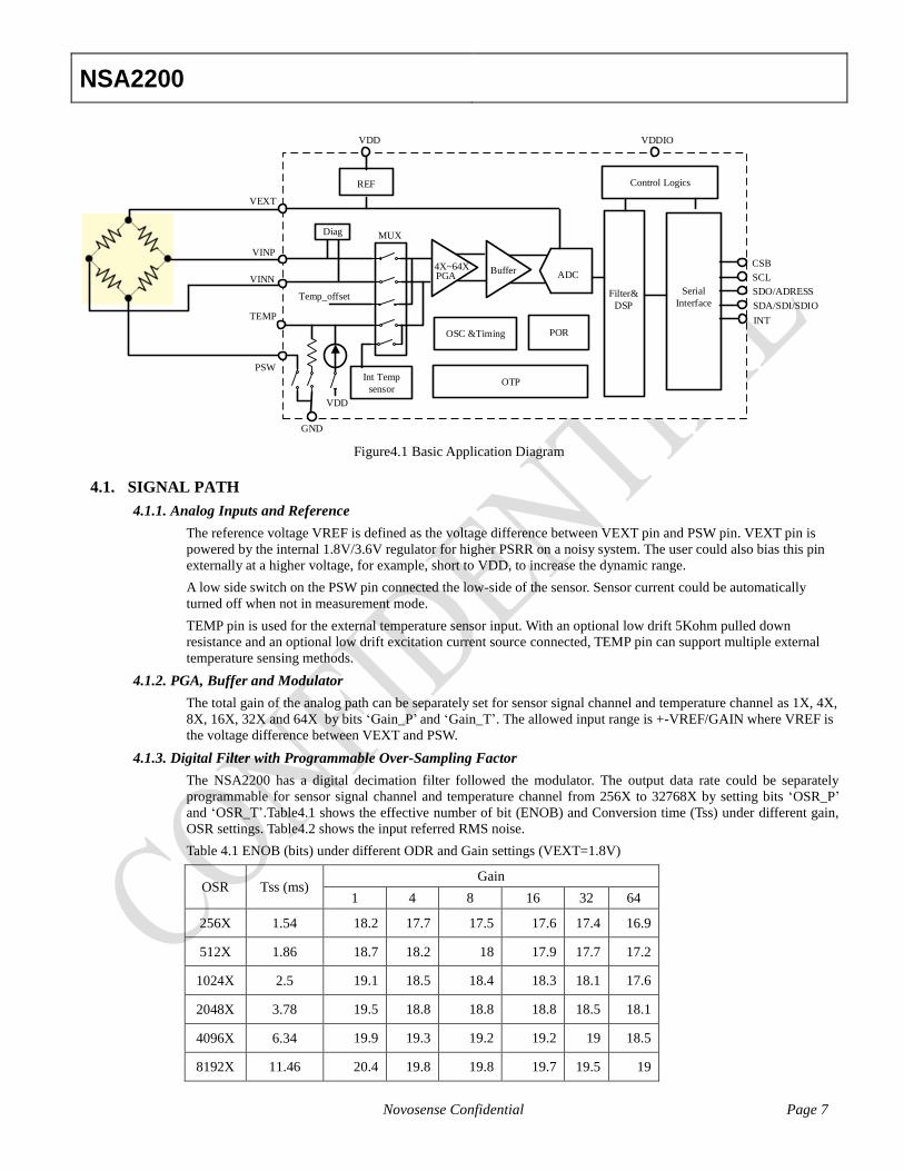
Figure4.1 Basic Application Diagram
4.1. SIGNAL PATH
4.1.1. Analog Inputs and Reference
The reference voltage VREF is defined as the voltage difference between VEXT pin and PSW pin. VEXT pin is
powered by the internal 1.8V/3.6V regulator for higher PSRR on a noisy system. The user could also bias this pin
externally at a higher voltage, for example, short to VDD, to increase the dynamic range.
A low side switch on the PSW pin connected the low-side of the sensor. Sensor current could be automatically
turned off when not in measurement mode.
TEMP pin is used for the external temperature sensor input. With an optional low drift 5Kohm pulled down
resistance and an optional low drift excitation current source connected, TEMP pin can support multiple external
temperature sensing methods.
4.1.2. PGA, Buffer and Modulator
The total gain of the analog path can be separately set for sensor signal channel and temperature channel as 1X, 4X,
8X, 16X, 32X and 64X by bits ‘Gain_P’ and ‘Gain_T’. The allowed input range is +-VREF/GAIN where VREF is
the voltage difference between VEXT and PSW.
4.1.3. Digital Filter with Programmable Over-Sampling Factor
The NSA2200 has a digital decimation filter followed the modulator. The output data rate could be separately
programmable for sensor signal channel and temperature channel from 256X to 32768X by setting bits ‘OSR_P’
and ‘OSR_T’.Table4.1 shows the effective number of bit (ENOB) and Conversion time (Tss) under different gain,
OSR settings. Table4.2 shows the input referred RMS noise.
Table 4.1 ENOB (bits) under different ODR and Gain settings (VEXT=1.8V)
OSR Tss (ms) Gain
1 4 8 16 32 64
256X 1.54 18.2 17.7 17.5 17.6 17.4 16.9
512X 1.86 18.7 18.2 18 17.9 17.7 17.2
1024X 2.5 19.1 18.5 18.4 18.3 18.1 17.6
2048X 3.78 19.5 18.8 18.8 18.8 18.5 18.1
4096X 6.34 19.9 19.3 19.2 19.2 19 18.5
8192X 11.46 20.4 19.8 19.8 19.7 19.5 19
NSA2200
Novosense Confidential Page 8
16384X 21.7 21 20.3 20.3 20.2 19.9 19.6
32768X 42.18 21.4 20.7 20.7 20.7 20.5 20
Table 4.2 Input Referred RMS noise (nV) under different ODR and Gain settings (VEXT=1.8V)
OSR Tss (ms) Gain
1 4 8 16 32 64
256X 1.54 16907.2 6406.6 3433.2 1601.7 985.9 650.5
512X 1.86 13732.9 5203.8 2788.6 1394.3 800.8 492.9
1024X 2.5 10407.6 3943.7 1971.9 1056.7 606.9 429.2
2048X 3.78 7359.3 2988.8 1494.4 747.2 459.9 325.2
4096X 6.34 5977.6 2265.1 1056.7 606.9 348.6 229.9
8192X 11.46 3943.7 1716.6 800.8 400.4 246.5 162.6
16384X 21.7 2788.6 1213.8 650.5 303.5 174.3 107.3
32768X 42.18 1971.9 800.8 528.3 200.2 132.1 81.3
4.1.4. Work Mode
4.1.4.1. Single-shot Sensor Signal Conversion
Setting ‘measurement_control’ = 01 and ‘sco’ = 1 to initiate once single-shot sensor signal conversion, the chip
powers up, performs once sensor signal conversion, and returns back to standby mode with automatically changing
‘sco’ to 0. INT goes high when data is ready and returns low after the data value (0x06-0x08) has been read out
from the ‘data_out’ registers. The ‘data_out’ registers can be read several times if required, even when the INT pin
is low, but care must be taken not to read data when the ‘data_out’ registers are just in refreshing.
The gain of the sensor signal conversion channel can be configured by the bits ‘Gain_P’ from 1X to 64X and the
OSR for the sensor conversion is configured by the ‘OSR_P’ bits from 256X to 32768X, the tradeoff of the
conversion time and the output RMS noise under different OSR settings is shown in table 4.1/4.2.
A following calibration DSP is optional during the single-shot sensor signal conversion. When the DSP is enabled
(‘raw_data_on’=0), a 24-bit calibrated sensor data will be stored in the ‘data_out’ registers after conversion ends,
and else, the raw 24-bit ADC output is stored there. The relationship between the raw ADC data and the input
signals for the sensor signal conversion is shown below:
23
_ _ ( )*2 * _ADC raw P
VINP VINNCNT Gain P
VREF
(‘unipolar’ = 0)
23 23
_ _ ( )*2 * _ 2ADC raw P
VINP VINNCNT Gain P
VREF
(‘unipolar’ = 1)
4.1.4.2. Single-shot Temperature Conversion
Different temperature sensing methods are supported by the NSA2200, either internally or externally. The
‘temp_sel’ bits support four configures for the temperature measurement. Set ‘temp_sel’ = 11 to choose the internal
temperature sensor.
For the external temperature sensing methods, the pin ‘TEMP’ is used as the temperature signal input and the other
end of the differential temperature signal pair is generated inside and can be configured by ‘T_offset_trim’ bits
from 0 to VEXT with an minimum step of 1/15VEXT (Table 4.3).
Table 4.3 Temp offset voltage under different ‘T_offset_trim’ settings
T_offset_trim T_offset_voltage
0000 0/15 VEXT
0001 1/15 VEXT
NSA2200
Novosense Confidential Page 9
0010 2/15VEXT
0011 3/15 VEXT
0100 4/15 VEXT
0101 5/15 VEXT
0110 6/15 VEXT
0111 7/15VEXT
1000 8/15 VEXT
1001 9/15 VEXT
1010 10/15 VEXT
1011 11/15 VEXT
1100 12/15 VEXT
1101 13/15 VEXT
1110 14/15 VEXT
1111 VEXT
During external temperature sensing, a low temperature drift 5Kohm pulled down resistance or a low temperature
drift excitation current source can be optional connected to the ‘TEMP’ pin to support multiple temperature sensing
methods. Typical applications for these temperature measurement methods are shown below. Rt could be either the
sensor bridge itself or a extra temperature sensing element close to the senor.
VDD
SDA/SDI/SDIO
SDO/ADRESS
VDDIO
ADC
REF
SCLCS
INTPGA Buffer
VINP
PSW
TEMP
VINN
GND
Temp_
offset
VDD
VEXT
Rt
GND
Rt_ref
DAC
Filter&
DSPSerial
Interface
NSA2200
Figure4.2 External Temperature sensing (‘temp_sel’== 00b)
NSA2200
Novosense Confidential Page 10
VDD
SDA/SDI/SDIO
SDO/ADRESS
VDDIO
ADC
REF
SCLCS
INTPGA Buffer
VINP
PSW
TEMP
VINN
GND
Temp_
offset
VDD
VEXT
Rt
DAC
Filter&
DSPSerial
Interface
NSA2200
Figure4.3 External temperature sensing with pull-down resistance connected (‘temp_sel’== 01b)
VDD
SDA/SDI/SDIO
SDO/ADRESS
VDDIO
ADC
REF
SCLCS
INTPGA Buffer
VINP
PSW
TEMP
VINN
GND
Temp_
offset
VDD
VEXT
Dt
DAC
Filter&
DSPSerial
Interface
NSA2200
Figure4.4 External temperature sensing with a 20uA current source connected (‘temp_sel’== 10b)
Setting ‘measurement_control’ = 00 and ‘sco’ = 1 to initiate once single-shot temperature conversion, the chip
powers up, performs once temperature conversion, and returns back to standby mode with automatically changing
‘sco’ to 0. When setting ‘raw_data_on’ = 0, the calibrated temperature data is stored in “temp_out” registers and
else, the raw ADC data of the temperature channel conversion would be stored in the “data_out” registers. INT pin
also goes high when the conversion ends and will return low after a reading of the “temp_out” or “data_out”
registers.
The gain of the external temperature conversion channel can be configured by the bits ‘Gain_T’ from 1X to 64X
and the gain of the internal temperature conversion channel is fixed. The OSR for the sensor conversion is
configured by the ‘OSR_T’ bits from 256X to 32768X.
4.1.4.3. Combined conversion
Setting ‘measurement_control’ = 10 and ‘sco’ = 1 to initiate once combined conversion, the chip powers up,
successively performs once temperature conversion and once sensor signal conversion, then returns back to standby
mode with automatically changing ‘sco’ to 0. The ‘raw_data_on’ bit should be set 0 during combined conversion
and the calibrated temperature data and sensor signal data are separately stored in ‘temp_out’ and ‘data_out’
registers. INT pin will go high when the sensor signal conversion ends and will return low after a reading of the
“data_out” registers.
The gain and OSR of the temperature channel and sensor signal channel are separately configured by the bits
‘Gain_P’, ‘OSR_P’, ‘Gain_T’ and ‘OSR_T’ just as the single shot conversions.
4.1.4.4. Sleep conversion
Setting ‘measurement_control’ = 11 and ‘sco’ = 1 to get into sleep conversion mode, the chip powers up and
periodically performs once temperature conversion, once sensor signal conversion and a period of sleep phase. The
duration of the sleep phase is configured by the ’sleep_time’ bits from 64ms to 1s. The chip will not get back to
standby mode until manually setting ‘sco’ bit to ‘0’. The ‘raw_data_on’ bit will be forced to 0 during sleep
conversion and the calibrated temperature data and sensor signal are separately stored in ‘temp_out’ and ‘data_out’
NSA2200
Novosense Confidential Page 11
registers. INT pin will go high when the sensor signal conversion ends and will automatically return low before
next temperature conversion starting or after a reading of the “data_out” registers.
The gain and OSR of the temperature channel and sensor signal channel are separately configured by the bits
‘Gain_P’, ‘OSR_P’, ‘Gain_T’ and ‘OSR_T’ just as the single shot conversions.
4.1.4.5. Diagnostic features
A suite of diagnostic features are provided on NSA2200 through six fault monitor comparators, refer to figure 4.5.
When diagnostics are enabled by set ‘diag_on’ to 1, two branches of 100nA current sources are added on the input
pair from sensor. This will add some voltage shift to the input signal but mostly common mode drift and any error
introduced could be minimized during sensor calibration. Four comparators are used to monitor if the voltage is in
100mV range of VEXT or ground. User could use this information to find out sensor faults like loss of bridge
positive, loss of bridge negative, open sensor connection and sensor input short.
The outputs of all the comparators are locked into the ‘Error_code<3:0>’ register at the end of every data
conversion. When either of the fault comparator outputs is asserted, indicating a fault, NSA2200 analog output
VOUT will be forced to a fault indicating voltage level of 2.5% of AVDD. Together with the lower or upper clip
limit function, system diagnostic can be performed to determine if the sensor is detective or the process being
monitored by the sensor is out of range.
PGA
VINP
VINN
100mV
Vext-100mV
100mV
A1
A2
Vext-100mV
INP_H
INP_L
INN_H
INN_L
Sensor NSA2200
Figure4.5 NSA2200 Fault Monitoring System
4.2. OTP
The NSA2200 contains 224 OTP bits. The lower 200 bits are released to customer to program the default configurations and
the sensor calibration coefficients, and the higher 24bits are reserved for internal trimming and will be pre-programmed in
factory. The reg0xbc and its corresponding OTP bits are used as OTP redundancy pointer, which can write one OTP bit
address and make this OTP bit functioning as programmed even if it has not been programmed or programming failed. E.g.
Writing Reg0xbc to 0x1a can make the 26P
thP OTP bit functioning as being programmed even if this OTP bit is not actually
programmed.
To program the OTP bits, please follow steps below:
1. Write all OTP registers what you want to program.
2. Switch the supply voltage on the VDD pin to 6.5V
3. Write Reg0x30 with 0x0C to enter OTP program mode
4. Write Reg0x6C with 01101010b to start OTP programming.
NSA2200
Novosense Confidential Page 12
5. Waiting 10ms
6. Switch the supply voltage on the VDD back to 2.5V
7. Write Reg0x6C with 00000001b to set the OTP read out margin.
8. Write Reg0x00 with 0x24 to soft reset the NSA2200
9. Read the OTP banks back to check if program succeeded.
4.3. SENSOR CALIBRATION
NSA2200 offers an on-chip calibration for sensor offset, sensitivity, temperature drift and non-linearity with the quotations
below and the maximum range for sensors that can be calibrated by NSA2200 is shown in table 4.4. To get the calibration
coefficient for a particular sensor, please contact Novosense customer support for coefficient calculating kits.
1 0 2 0 0 1 0
2 2
0 2 0( ( ( ) ( ) ))*( ( ) ( ) )osen ffseP CNT CTC T CTC T S STC TP CNT T T T TSTC T
0
2 3
0 00( ) ( ) ( )s ssP P PP P K P K PP
Table4.4 Maximum range of sensors allowed for NSA2200
Symbol Description Min Max Unit
Vfs Full Span +/-0.001 +/-1 V/V
STC1 1P
stP temp drift for sensitivity -0.0078 0.0078 Vfs/℃
STC2 2P
ndP temp drift for sensitivity -1.5e-5 1.5e-5 Vfs/℃P
2P
Voff Sensor offset -1/GAIN < Voff+Vfs < 1/GAIN V/V
CTC1 1P
stP temp drift for Offset -0.0078 0.0078 V/V/℃
CTC2 2P
ndP temp drift for Offset -1.5e-5 1.5e-5 V/V/℃P
2P
Ks 2nd order non-linearity -0.25 0.25 1/Vfs
Kss 2nd order non-linearity -0.25 0.25 1/Vfs
Also, NSA2200 offers an on-chip calibration for both external and internal temperature sensing methods. After calibration,
the NSA2200 can offer an real time temperature value of +/- 1℃ accuracy with the built-in temperature sensor during -40℃
and 85℃. Please contact Novosense customer support for coefficient calculating kits.
5.0 SPI INTERFACE NSA2200 provides both SPI and I2C interface for serial communication and ‘CSB’ pin is used to switch between these two
protocols. Pulling ‘CSB’ pin low selects the SPI interface, leaving ‘CSB’ pin float or puling it high selects the I2C interface.
5.1. INTERFACE SPECIFICATION
Table 5.1 SPI interface specifications
Symbol Parameter Condition Min Max Unit
fBsclkB Clock frequency Max load on SDIO or
SDO = 25pF 10 MHz
tBsclk_lB SLCK low pulse 20 Ns
tBsclk_hB SLCK high pulse 20
TBsdi_setupB SDI setup time 20 ns
TBsdi_holdB SDI hold time 20 ns
TBsdo_odB SDO/SDI output delay Load = 25pF 30 ns
NSA2200
Novosense Confidential Page 13
Load = 250pF 40 ns
TBcsb_setupB CSB setup time 20 ns
TBcsb_holdB CSB hold time 40 ns
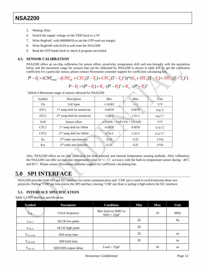
The figure below shows the definition of the SPI timing given in table 5.1
Figure 5.1 SPI timing diagram
The falling edge of CSB, in conjunction with the rising edge of SCLK, determines the start of framing. Once the beginning of the
frame has been determined, timing is straightforward. The first phase of the transfer is the instruction phase, which consists of 16 bits
followed by data that can be of variable lengths in multiples of 8 bits. If the device is configured with CSB tied low, framing begins
with the first rising edge of SCLK.
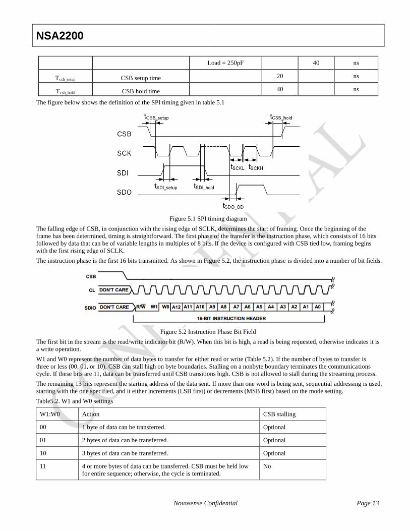
The instruction phase is the first 16 bits transmitted. As shown in Figure 5.2, the instruction phase is divided into a number of bit fields.
Figure 5.2 Instruction Phase Bit Field
The first bit in the stream is the read/write indicator bit (R/W). When this bit is high, a read is being requested, otherwise indicates it is
a write operation.
W1 and W0 represent the number of data bytes to transfer for either read or write (Table 5.2). If the number of bytes to transfer is
three or less (00, 01, or 10), CSB can stall high on byte boundaries. Stalling on a nonbyte boundary terminates the communications
cycle. If these bits are 11, data can be transferred until CSB transitions high. CSB is not allowed to stall during the streaming process.
The remaining 13 bits represent the starting address of the data sent. If more than one word is being sent, sequential addressing is used,
starting with the one specified, and it either increments (LSB first) or decrements (MSB first) based on the mode setting.
Table5.2. W1 and W0 settings
W1:W0 Action CSB stalling
00 1 byte of data can be transferred. Optional
01 2 bytes of data can be transferred. Optional
10 3 bytes of data can be transferred. Optional
11 4 or more bytes of data can be transferred. CSB must be held low
for entire sequence; otherwise, the cycle is terminated.
No
NSA2200
Novosense Confidential Page 14
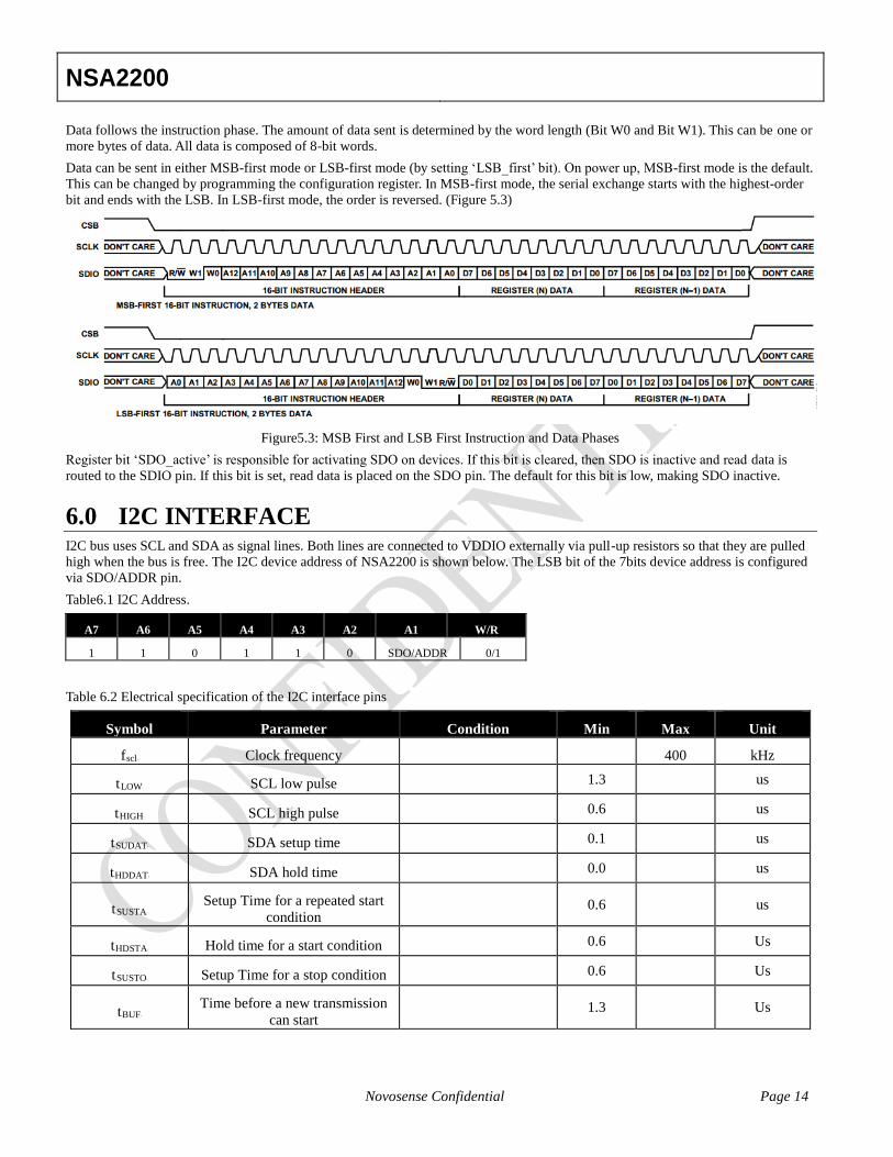
Data follows the instruction phase. The amount of data sent is determined by the word length (Bit W0 and Bit W1). This can be one or
more bytes of data. All data is composed of 8-bit words.
Data can be sent in either MSB-first mode or LSB-first mode (by setting ‘LSB_first’ bit). On power up, MSB-first mode is the default.
This can be changed by programming the configuration register. In MSB-first mode, the serial exchange starts with the highest-order
bit and ends with the LSB. In LSB-first mode, the order is reversed. (Figure 5.3)
Figure5.3: MSB First and LSB First Instruction and Data Phases
Register bit ‘SDO_active’ is responsible for activating SDO on devices. If this bit is cleared, then SDO is inactive and read data is
routed to the SDIO pin. If this bit is set, read data is placed on the SDO pin. The default for this bit is low, making SDO inactive.
6.0 I2C INTERFACE I2C bus uses SCL and SDA as signal lines. Both lines are connected to VDDIO externally via pull-up resistors so that they are pulled
high when the bus is free. The I2C device address of NSA2200 is shown below. The LSB bit of the 7bits device address is configured
via SDO/ADDR pin.
Table6.1 I2C Address.
A7 A6 A5 A4 A3 A2 A1 W/R
1 1 0 1 1 0 SDO/ADDR 0/1
Table 6.2 Electrical specification of the I2C interface pins
Symbol Parameter Condition Min Max Unit
fBsclB Clock frequency 400 kHz
tBLOWB SCL low pulse 1.3 us
tBHIGHB SCL high pulse 0.6 us
tBSUDATB SDA setup time 0.1 us
tBHDDATB SDA hold time 0.0 us
tBSUSTAB
Setup Time for a repeated start
condition 0.6 us
tBHDSTAB Hold time for a start condition 0.6 Us
tBSUSTOB Setup Time for a stop condition 0.6 Us
tBBUFB
Time before a new transmission
can start 1.3 Us
NSA2200
Novosense Confidential Page 15
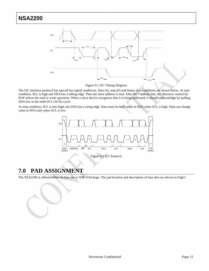
Figure 6.1 I2C Timing Diagram
The I2C interface protocol has special bus signal conditions. Start (S), stop (P) and binary data conditions are shown below. At start
condition, SCL is high and SDA has a falling edge. Then the slave address is sent. After the 7 address bits, the direction control bit
R/W selects the read or write operation. When a slave device recognizes that it is being addressed, it should acknowledge by pulling
SDA low in the ninth SCL (ACK) cycle.
At stop condition, SCL is also high, but SDA has a rising edge. Data must be held stable at SDA when SCL is high. Data can change
value at SDA only when SCL is low.
Figure 6.2 I2C Protocol
7.0 PAD ASSIGNMENT The NSA2200 is offered either via bare die or SOP-8 Package. The pad location and description of bare dies are shown in Fig8.1
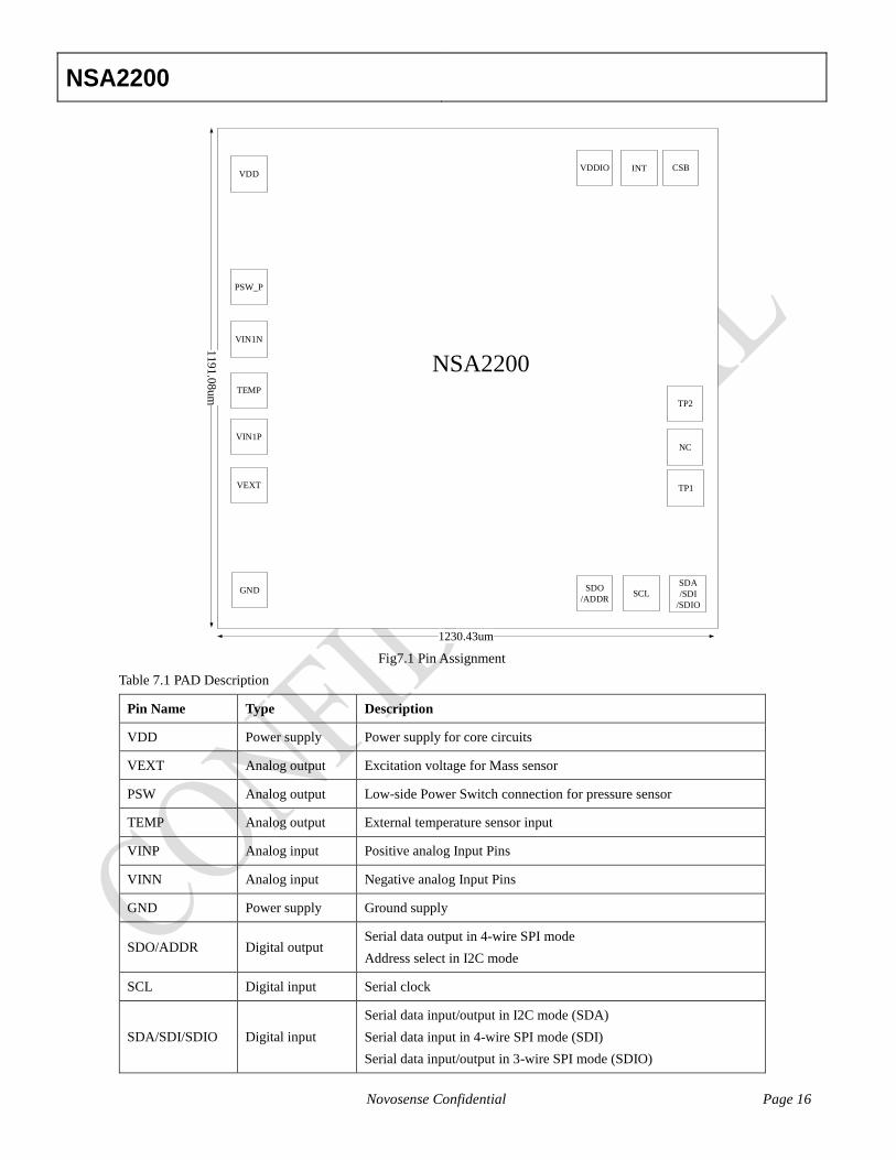
NSA2200
Novosense Confidential Page 16
PSW_P
NSA2200
VIN1N
TEMP
VIN1P
VEXT
VDD
GND SDO
/ADDRSCL
SDA
/SDI
/SDIO
VDDIO CSBINT
NC
TP2
11
91.0
8u
m
1230.43um
TP1
Fig7.1 Pin Assignment
Table 7.1 PAD Description
Pin Name Type Description
VDD Power supply Power supply for core circuits
VEXT Analog output Excitation voltage for Mass sensor
PSW Analog output Low-side Power Switch connection for pressure sensor
TEMP Analog output External temperature sensor input
VINP Analog input Positive analog Input Pins
VINN Analog input Negative analog Input Pins
GND Power supply Ground supply
SDO/ADDR Digital output Serial data output in 4-wire SPI mode
Address select in I2C mode
SCL Digital input Serial clock
SDA/SDI/SDIO Digital input
Serial data input/output in I2C mode (SDA)
Serial data input in 4-wire SPI mode (SDI)
Serial data input/output in 3-wire SPI mode (SDIO)

NSA2200
Novosense Confidential Page 17
INT Digital output Interrupt output (data ready)
CSB Digital input Chip select
VDDIO Power supply Power Supply for I/O Circuit
TP1 Analog output Test pad, internal use
TP2 Analog Output Test Pad, internal use
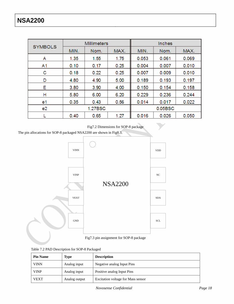
The NSA2200 is also offered via SOP-8 package, the dimensions are shown in fig8.2 Note that, only SPI serial interface can not be
used in the packaged version.
NSA2200
Novosense Confidential Page 18
Fig7.2 Dimensions for SOP-8 package
The pin allocations for SOP-8 packaged NSA2200 are shown in Fig8.3.
VINN
VINP
VEXT
GND
VDD
NC
SDA
SCL
NSA2200
Fig7.3 pin assignment for SOP-8 package
Table 7.2 PAD Description for SOP-8 Packaged
Pin Name Type Description
VINN Analog input Negative analog Input Pins
VINP Analog input Positive analog Input Pins
VEXT Analog output Excitation voltage for Mass sensor
NSA2200
Novosense Confidential Page 19
GND Analog input Ground supply
SCL Digital input Serial clock
SDA Digital input Serial data input/output in I2C mode (SDA)
NC NC NC
VDD Power supply Power supply for both core and IO circuits
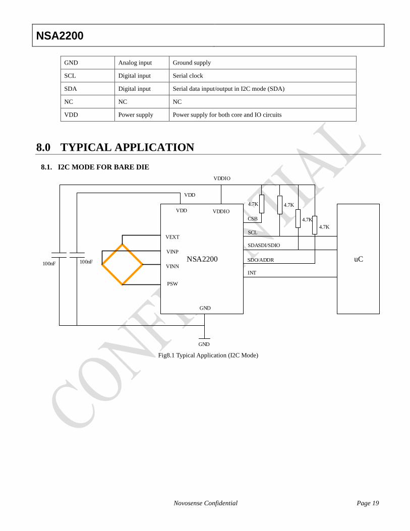
8.0 TYPICAL APPLICATION
8.1. I2C MODE FOR BARE DIE
NSA2200
VDD VDDIO
SCL
CSB
SDASDI/SDIO
SDO/ADDR
INT
GND
uC100nF100nF
4.7K
4.7K
4.7K
VEXT
VINP
VINN
PSW
GND
4.7K
VDD
VDDIO
Fig8.1 Typical Application (I2C Mode)
NSA2200
Novosense Confidential Page 20
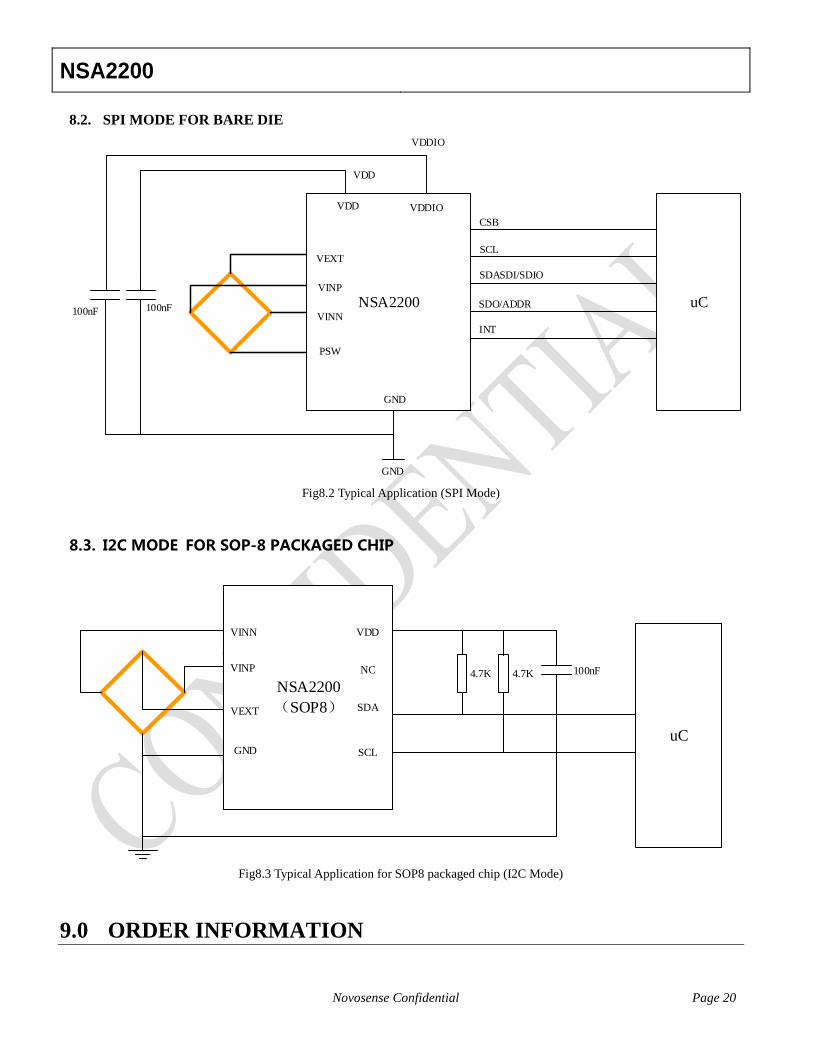
8.2. SPI MODE FOR BARE DIE
NSA2200
VDD VDDIO
SCL
CSB
SDASDI/SDIO
SDO/ADDR
INT
GND
uC100nF100nF
VEXT
VINP
VINN
PSW
GND
VDD
VDDIO
Fig8.2 Typical Application (SPI Mode)
8.3. I2C MODE FOR SOP-8 PACKAGED CHIP
NSA2200
(SOP8)
VDD
GND
uC
100nF4.7K 4.7K
VEXT
VINP
VINN
NC
SDA
SCL
Fig8.3 Typical Application for SOP8 packaged chip (I2C Mode)
9.0 ORDER INFORMATION
NSA2200
Novosense Confidential Page 21
Part NO Unit Description
NSA2200_B pcs Bare die
NSA2200_P pcs SOP-8 packaged
10.0 DOCUMENT HISTORY AND MODIFICATION
Revision Description Date
1.1 Translated from V1.6 2015-4-16