PXIe-5122 Specifications - National Instruments · 20 V — 6 mVrms (0.030% FS) Figure 3....
22
SPECIFICATIONS PXIe-5122 100 MHz, 100 MS/s, 14-Bit PXI Express Oscilloscope Contents Definitions................................................................................................................................. 2 Conditions................................................................................................................................. 2 Vertical...................................................................................................................................... 2 Analog Input..................................................................................................................... 2 Impedance and Coupling.................................................................................................. 3 Voltage Levels................................................................................................................... 3 Accuracy........................................................................................................................... 3 Bandwidth and Transient Response.................................................................................. 4 Spectral Characteristics..................................................................................................... 6 Horizontal................................................................................................................................10 Sample Clock.................................................................................................................. 10 Phase-Locked Loop (PLL) Reference Clock.................................................................. 11 CLK IN (Sample Clock and Reference Clock Input)..................................................... 12 CLK OUT (Sample Clock and Reference Clock Output)...............................................12 Trigger..................................................................................................................................... 13 Reference (Stop) Trigger................................................................................................. 13 External Trigger.............................................................................................................. 15 Programmable Function Interface (PFI 0 and PFI 1).............................................................. 15 Waveform................................................................................................................................ 16 Calibration............................................................................................................................... 17 External Calibration........................................................................................................ 17 Self-Calibration............................................................................................................... 17 Calibration Specifications............................................................................................... 17 Software.................................................................................................................................. 17 Driver Software............................................................................................................... 17 Application Software...................................................................................................... 17 Interactive Soft Front Panel and Configuration.............................................................. 17 TClk Specifications......................................................................................................... 18 Power...................................................................................................................................... 18 Dimensions and Weight.......................................................................................................... 19 Environment............................................................................................................................ 19 Operating Environment................................................................................................... 19 Storage Environment.......................................................................................................19
-
Upload
duongthien -
Category
Documents
-
view
224 -
download
0
Transcript of PXIe-5122 Specifications - National Instruments · 20 V — 6 mVrms (0.030% FS) Figure 3....
SPECIFICATIONS
PXIe-5122100 MHz, 100 MS/s, 14-Bit PXI Express Oscilloscope
ContentsDefinitions.................................................................................................................................2Conditions................................................................................................................................. 2Vertical...................................................................................................................................... 2
Analog Input..................................................................................................................... 2Impedance and Coupling.................................................................................................. 3Voltage Levels...................................................................................................................3Accuracy........................................................................................................................... 3Bandwidth and Transient Response.................................................................................. 4Spectral Characteristics.....................................................................................................6
Horizontal................................................................................................................................10Sample Clock.................................................................................................................. 10Phase-Locked Loop (PLL) Reference Clock.................................................................. 11CLK IN (Sample Clock and Reference Clock Input)..................................................... 12CLK OUT (Sample Clock and Reference Clock Output)...............................................12
Trigger.....................................................................................................................................13Reference (Stop) Trigger.................................................................................................13External Trigger.............................................................................................................. 15
Programmable Function Interface (PFI 0 and PFI 1)..............................................................15Waveform................................................................................................................................16Calibration...............................................................................................................................17
External Calibration........................................................................................................ 17Self-Calibration...............................................................................................................17Calibration Specifications............................................................................................... 17
Software.................................................................................................................................. 17Driver Software...............................................................................................................17Application Software...................................................................................................... 17Interactive Soft Front Panel and Configuration.............................................................. 17TClk Specifications.........................................................................................................18
Power...................................................................................................................................... 18Dimensions and Weight.......................................................................................................... 19Environment............................................................................................................................19
Operating Environment...................................................................................................19Storage Environment.......................................................................................................19
Shock and Vibration................................................................................................................20Compliance and Certifications................................................................................................20
Safety.............................................................................................................................. 20Electromagnetic Compatibility....................................................................................... 20CE Compliance .............................................................................................................. 21Online Product Certification........................................................................................... 21Environmental Management........................................................................................... 21
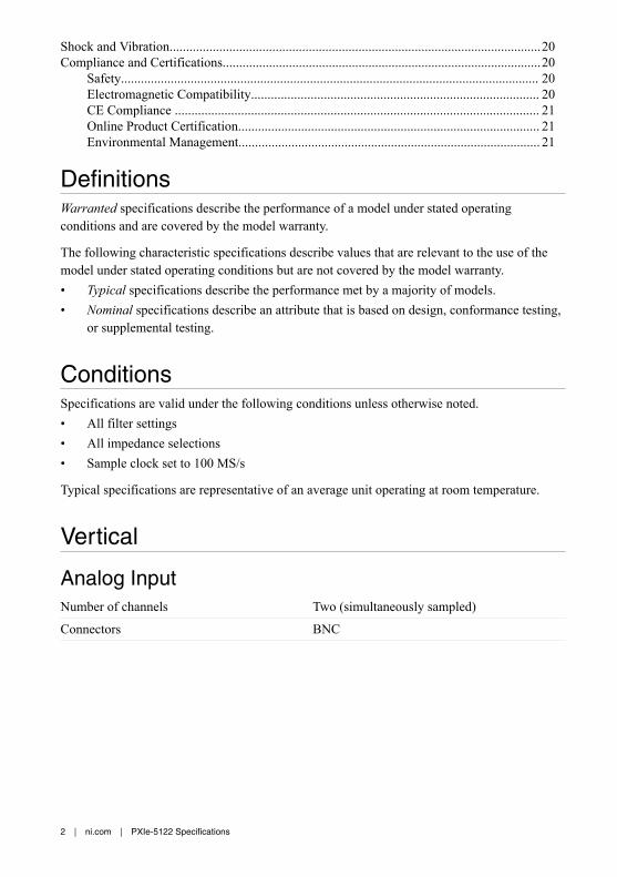
DefinitionsWarranted specifications describe the performance of a model under stated operatingconditions and are covered by the model warranty.
The following characteristic specifications describe values that are relevant to the use of themodel under stated operating conditions but are not covered by the model warranty.• Typical specifications describe the performance met by a majority of models.• Nominal specifications describe an attribute that is based on design, conformance testing,
or supplemental testing.
ConditionsSpecifications are valid under the following conditions unless otherwise noted.• All filter settings• All impedance selections• Sample clock set to 100 MS/s
Typical specifications are representative of an average unit operating at room temperature.
Vertical
Analog InputNumber of channels Two (simultaneously sampled)
Connectors BNC
2 | ni.com | PXIe-5122 Specifications
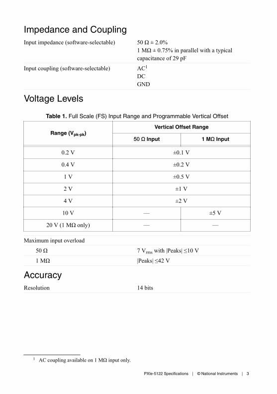
Impedance and CouplingInput impedance (software-selectable) 50 Ω ± 2.0%
1 MΩ ± 0.75% in parallel with a typicalcapacitance of 29 pF
Input coupling (software-selectable) AC1
DCGND
Voltage Levels
Table 1. Full Scale (FS) Input Range and Programmable Vertical Offset
Range (Vpk-pk)Vertical Offset Range
50 Ω Input 1 MΩ Input
0.2 V ±0.1 V
0.4 V ±0.2 V
1 V ±0.5 V
2 V ±1 V
4 V ±2 V
10 V — ±5 V
20 V (1 MΩ only) — —
Maximum input overload
50 Ω 7 Vrms with |Peaks| ≤10 V
1 MΩ |Peaks| ≤42 V
AccuracyResolution 14 bits
1 AC coupling available on 1 MΩ input only.
PXIe-5122 Specifications | © National Instruments | 3
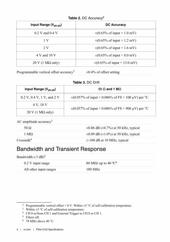
Table 2. DC Accuracy2
Input Range (Vpk-pk) DC Accuracy
0.2 V and 0.4 V ±(0.65% of input + 1.0 mV)
1 V ±(0.65% of input + 1.2 mV)
2 V ±(0.65% of input + 1.6 mV)
4 V and 10 V ±(0.65% of input + 8.0 mV)
20 V (1 MΩ only) ±(0.65% of input + 13.0 mV)
Programmable vertical offset accuracy3 ±0.4% of offset setting
Table 3. DC Drift
Input Range (Vpk-pk) 50 Ω and 1 MΩ
0.2 V, 0.4 V, 1 V, and 2 V ±(0.057% of input + 0.006% of FS + 100 μV) per °C
4 V, 10 V±(0.057% of input + 0.006% of FS + 900 µV) per °C
20 V (1 MΩ only)
AC amplitude accuracy3
50 Ω ±0.06 dB (±0.7%) at 50 kHz, typical
1 MΩ ±0.09 dB (±1.0%) at 50 kHz, typicalCrosstalk4 ≤-100 dB at 10 MHz, typical
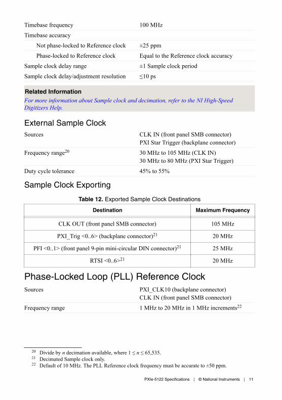
Bandwidth and Transient ResponseBandwidth (-3 dB)5
0.2 V input range 80 MHz up to 40 ºC6
All other input ranges 100 MHz
2 Programmable vertical offset = 0 V. Within ±5 °C of self-calibration temperature.3 Within ±5 °C of self-calibration temperature.4 CH 0 to/from CH 1 and External Trigger to CH 0 or CH 1.5 Filters off.6 78 MHz above 40 °C.
4 | ni.com | PXIe-5122 Specifications
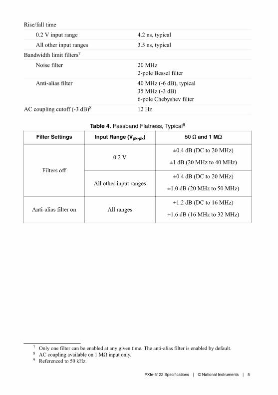
Rise/fall time
0.2 V input range 4.2 ns, typical
All other input ranges 3.5 ns, typicalBandwidth limit filters7
Noise filter 20 MHz2-pole Bessel filter
Anti-alias filter 40 MHz (-6 dB), typical35 MHz (-3 dB)6-pole Chebyshev filter
AC coupling cutoff (-3 dB)8 12 Hz
Table 4. Passband Flatness, Typical9
Filter Settings Input Range (Vpk-pk) 50 Ω and 1 MΩ
Filters off
0.2 V±0.4 dB (DC to 20 MHz)
±1 dB (20 MHz to 40 MHz)
All other input ranges±0.4 dB (DC to 20 MHz)
±1.0 dB (20 MHz to 50 MHz)
Anti-alias filter on All ranges±1.2 dB (DC to 16 MHz)
±1.6 dB (16 MHz to 32 MHz)
7 Only one filter can be enabled at any given time. The anti-alias filter is enabled by default.8 AC coupling available on 1 MΩ input only.9 Referenced to 50 kHz.
PXIe-5122 Specifications | © National Instruments | 5
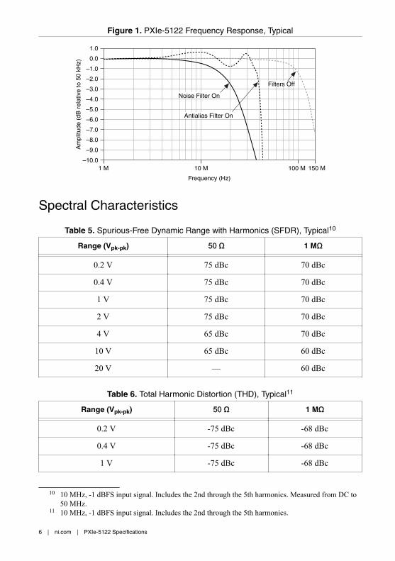
Figure 1. PXIe-5122 Frequency Response, Typical
Frequency (Hz)
150 M100 M10 M1 M–10.0
–9.0
–8.0
–7.0
–6.0
–5.0
–4.0
–3.0
–2.0
–1.0
0.0
1.0
Am
plitu
de (
dB r
elat
ive
to 5
0 kH
z)
Noise Filter On
Antialias Filter On
Filters Off
Spectral Characteristics
Table 5. Spurious-Free Dynamic Range with Harmonics (SFDR), Typical10
Range (Vpk-pk) 50 Ω 1 MΩ
0.2 V 75 dBc 70 dBc
0.4 V 75 dBc 70 dBc
1 V 75 dBc 70 dBc
2 V 75 dBc 70 dBc
4 V 65 dBc 70 dBc
10 V 65 dBc 60 dBc
20 V — 60 dBc
Table 6. Total Harmonic Distortion (THD), Typical11
Range (Vpk-pk) 50 Ω 1 MΩ
0.2 V -75 dBc -68 dBc
0.4 V -75 dBc -68 dBc
1 V -75 dBc -68 dBc
10 10 MHz, -1 dBFS input signal. Includes the 2nd through the 5th harmonics. Measured from DC to50 MHz.
11 10 MHz, -1 dBFS input signal. Includes the 2nd through the 5th harmonics.
6 | ni.com | PXIe-5122 Specifications
Table 6. Total Harmonic Distortion (THD), Typical11 (Continued)
Range (Vpk-pk) 50 Ω 1 MΩ
2 V -73 dBc -68 dBc
4 V -63 dBc -68 dBc
10 V -63 dBc -58 dBc
20 V — -58 dBc
Intermodulation distortion12 -75 dBc, typical
Table 7. Signal-to-Noise Ratio (SNR), Typical13
Range (Vpk-pk)50 Ω 1 MΩ
Filters Off Anti-alias Filter On Filters Off Anti-alias Filter On
0.2 V 60 dB 60 dB 56 dB 60 dB
0.4 V 62 dB 62 dB 61 dB 62 dB
1 V 62 dB 62 dB 62 dB 62 dB
2 V 62 dB 62 dB 62 dB 62 dB
4 V — — 61 dB 62 dB
Table 8. Signal to Noise and Distortion (SINAD), Typical14
Range (Vpk-pk)50 Ω 1 MΩ
Filters Off Anti-alias Filter On Filters Off Anti-alias Filter On
0.2 V 60 dB 60 dB 56 dB 59 dB
0.4 V 62 dB 62 dB 60 dB 61 dB
1 V 62 dB 62 dB 61 dB 61 dB
2 V 62 dB 62 dB 61 dB 61 dB
4 V — — 60 dB 61 dB
11 10 MHz, -1 dBFS input signal. Includes the 2nd through the 5th harmonics.12 0.2 V to 2.0 V input range. 50 Ω input impedance. Two tones at 10.2 MHz and 11.2 MHz. Each
tone is -7 dBFS.13 10 MHz, -1 dBFS input signal. Excludes harmonics. Measured from DC to 50 MHz.14 10 MHz, -1 dBFS input signal. Includes harmonics. Measured from DC to 50 MHz.
PXIe-5122 Specifications | © National Instruments | 7
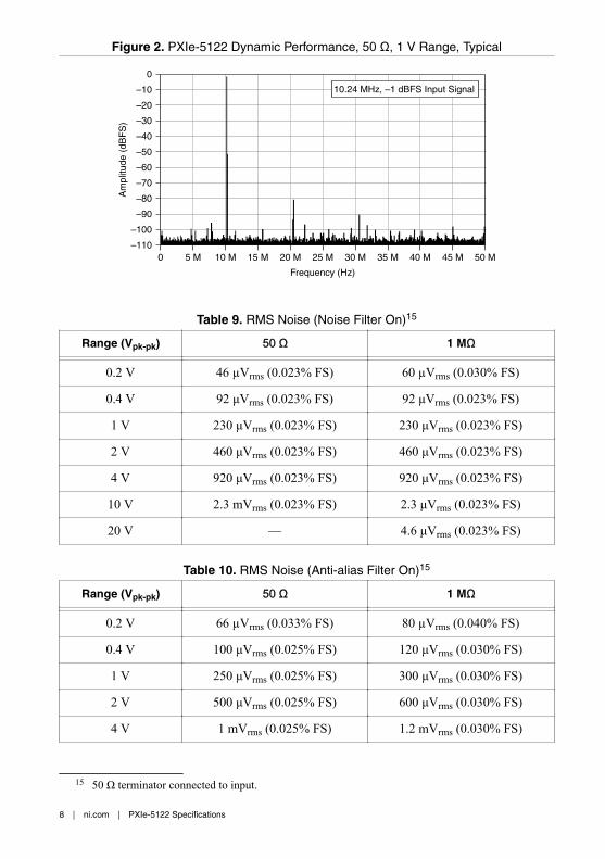
Figure 2. PXIe-5122 Dynamic Performance, 50 Ω, 1 V Range, Typical
–110
–100
–90
–80
–70
–60
–50
–40
–30
–20
–10
0
Am
plitu
de (
dBF
S)
Frequency (Hz)
50 M45 M40 M35 M30 M25 M20 M15 M10 M5 M0
10.24 MHz, –1 dBFS Input Signal
Table 9. RMS Noise (Noise Filter On)15
Range (Vpk-pk) 50 Ω 1 MΩ
0.2 V 46 µVrms (0.023% FS) 60 µVrms (0.030% FS)
0.4 V 92 μVrms (0.023% FS) 92 μVrms (0.023% FS)
1 V 230 μVrms (0.023% FS) 230 μVrms (0.023% FS)
2 V 460 μVrms (0.023% FS) 460 μVrms (0.023% FS)
4 V 920 μVrms (0.023% FS) 920 μVrms (0.023% FS)
10 V 2.3 mVrms (0.023% FS) 2.3 μVrms (0.023% FS)
20 V — 4.6 μVrms (0.023% FS)
Table 10. RMS Noise (Anti-alias Filter On)15
Range (Vpk-pk) 50 Ω 1 MΩ
0.2 V 66 µVrms (0.033% FS) 80 µVrms (0.040% FS)
0.4 V 100 μVrms (0.025% FS) 120 μVrms (0.030% FS)
1 V 250 μVrms (0.025% FS) 300 μVrms (0.030% FS)
2 V 500 μVrms (0.025% FS) 600 μVrms (0.030% FS)
4 V 1 mVrms (0.025% FS) 1.2 mVrms (0.030% FS)
15 50 Ω terminator connected to input.
8 | ni.com | PXIe-5122 Specifications
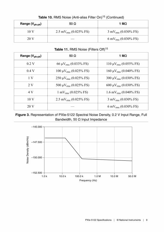
Table 10. RMS Noise (Anti-alias Filter On)15 (Continued)
Range (Vpk-pk) 50 Ω 1 MΩ
10 V 2.5 mVrms (0.025% FS) 3 mVrms (0.030% FS)
20 V — 6 mVrms (0.030% FS)
Table 11. RMS Noise (Filters Off)15
Range (Vpk-pk) 50 Ω 1 MΩ
0.2 V 66 µVrms (0.033% FS) 110 μVrms (0.055% FS)
0.4 V 100 μVrms (0.025% FS) 160 μVrms (0.040% FS)
1 V 250 μVrms (0.025% FS) 300 μVrms (0.030% FS)
2 V 500 μVrms (0.025% FS) 600 μVrms (0.030% FS)
4 V 1 mVrms (0.025% FS) 1.6 mVrms (0.040% FS)
10 V 2.5 mVrms (0.025% FS) 3 mVrms (0.030% FS)
20 V — 6 mVrms (0.030% FS)
Figure 3. Representation of PXIe-5122 Spectral Noise Density, 0.2 V Input Range, FullBandwidth, 50 Ω Input Impedance
–145.000
–147.500
–150.000
–152.5001.0 k 10.0 k 100.0 k 1.0 M 10.0 M 50.0 M
Frequency (Hz)
Noi
se D
ensi
ty (
dBm
/Hz)
PXIe-5122 Specifications | © National Instruments | 9
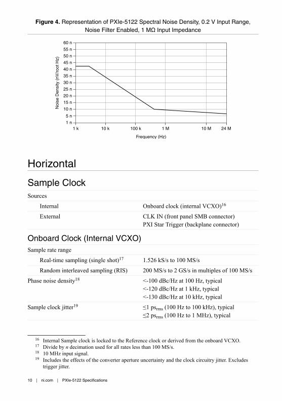
Figure 4. Representation of PXIe-5122 Spectral Noise Density, 0.2 V Input Range,Noise Filter Enabled, 1 MΩ Input Impedance
60 n
50 n
40 n
30 n
20 n
10 n
1 n1 k 10 k 100 k 1 M 10 M 24 M
Frequency (Hz)
Noi
se D
ensi
ty (
nV/r
oot H
z)
5 n
15 n
55 n
25 n
35 n
45 n
Horizontal
Sample ClockSources
Internal Onboard clock (internal VCXO)16
External CLK IN (front panel SMB connector)PXI Star Trigger (backplane connector)
Onboard Clock (Internal VCXO)Sample rate range
Real-time sampling (single shot)17 1.526 kS/s to 100 MS/s
Random interleaved sampling (RIS) 200 MS/s to 2 GS/s in multiples of 100 MS/s
Phase noise density18 <-100 dBc/Hz at 100 Hz, typical<-120 dBc/Hz at 1 kHz, typical<-130 dBc/Hz at 10 kHz, typical
Sample clock jitter19 ≤1 psrms (100 Hz to 100 kHz), typical≤2 psrms (100 Hz to 1 MHz), typical
16 Internal Sample clock is locked to the Reference clock or derived from the onboard VCXO.17 Divide by n decimation used for all rates less than 100 MS/s.18 10 MHz input signal.19 Includes the effects of the converter aperture uncertainty and the clock circuitry jitter. Excludes
trigger jitter.
10 | ni.com | PXIe-5122 Specifications
Timebase frequency 100 MHz
Timebase accuracy
Not phase-locked to Reference clock ±25 ppm
Phase-locked to Reference clock Equal to the Reference clock accuracy
Sample clock delay range ±1 Sample clock period
Sample clock delay/adjustment resolution ≤10 ps
Related InformationFor more information about Sample clock and decimation, refer to the NI High-SpeedDigitizers Help.
External Sample ClockSources CLK IN (front panel SMB connector)
PXI Star Trigger (backplane connector)
Frequency range20 30 MHz to 105 MHz (CLK IN)30 MHz to 80 MHz (PXI Star Trigger)
Duty cycle tolerance 45% to 55%
Sample Clock Exporting
Table 12. Exported Sample Clock Destinations
Destination Maximum Frequency
CLK OUT (front panel SMB connector) 105 MHz
PXI_Trig <0..6> (backplane connector)21 20 MHz
PFI <0..1> (front panel 9-pin mini-circular DIN connector)21 25 MHz
RTSI <0..6>21 20 MHz
Phase-Locked Loop (PLL) Reference ClockSources PXI_CLK10 (backplane connector)
CLK IN (front panel SMB connector)
Frequency range 1 MHz to 20 MHz in 1 MHz increments22
20 Divide by n decimation available, where 1 ≤ n ≤ 65,535.21 Decimated Sample clock only.22 Default of 10 MHz. The PLL Reference clock frequency must be accurate to ±50 ppm.
PXIe-5122 Specifications | © National Instruments | 11
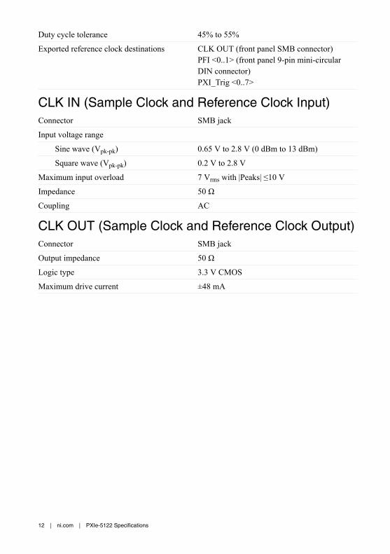
Duty cycle tolerance 45% to 55%
Exported reference clock destinations CLK OUT (front panel SMB connector)PFI <0..1> (front panel 9-pin mini-circularDIN connector)PXI_Trig <0..7>
CLK IN (Sample Clock and Reference Clock Input)Connector SMB jack
Input voltage range
Sine wave (Vpk-pk) 0.65 V to 2.8 V (0 dBm to 13 dBm)
Square wave (Vpk-pk) 0.2 V to 2.8 V
Maximum input overload 7 Vrms with |Peaks| ≤10 V
Impedance 50 Ω
Coupling AC
CLK OUT (Sample Clock and Reference Clock Output)Connector SMB jack
Output impedance 50 Ω
Logic type 3.3 V CMOS
Maximum drive current ±48 mA
12 | ni.com | PXIe-5122 Specifications
Trigger
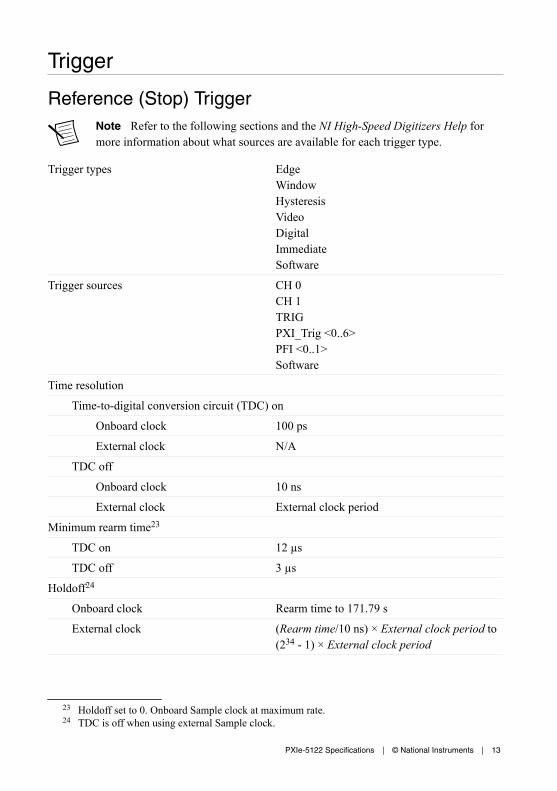
Reference (Stop) TriggerNote Refer to the following sections and the NI High-Speed Digitizers Help formore information about what sources are available for each trigger type.
Trigger types EdgeWindowHysteresisVideoDigitalImmediateSoftware
Trigger sources CH 0CH 1TRIGPXI_Trig <0..6>PFI <0..1>Software
Time resolution
Time-to-digital conversion circuit (TDC) on
Onboard clock 100 ps
External clock N/A
TDC off
Onboard clock 10 ns
External clock External clock period
Minimum rearm time23
TDC on 12 µs
TDC off 3 µs
Holdoff24
Onboard clock Rearm time to 171.79 s
External clock (Rearm time/10 ns) × External clock period to(234 - 1) × External clock period
23 Holdoff set to 0. Onboard Sample clock at maximum rate.24 TDC is off when using external Sample clock.
PXIe-5122 Specifications | © National Instruments | 13
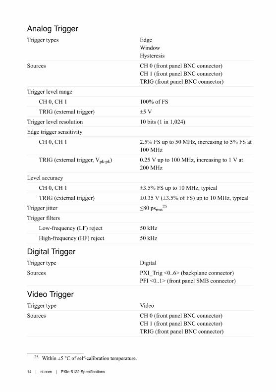
Analog TriggerTrigger types Edge
WindowHysteresis
Sources CH 0 (front panel BNC connector)CH 1 (front panel BNC connector)TRIG (front panel BNC connector)
Trigger level range
CH 0, CH 1 100% of FS
TRIG (external trigger) ±5 V
Trigger level resolution 10 bits (1 in 1,024)
Edge trigger sensitivity
CH 0, CH 1 2.5% FS up to 50 MHz, increasing to 5% FS at100 MHz
TRIG (external trigger, Vpk-pk) 0.25 V up to 100 MHz, increasing to 1 V at200 MHz
Level accuracy
CH 0, CH 1 ±3.5% FS up to 10 MHz, typical
TRIG (external trigger) ±0.35 V (±3.5% of FS) up to 10 MHz, typical
Trigger jitter ≤80 psrms25
Trigger filters
Low-frequency (LF) reject 50 kHz
High-frequency (HF) reject 50 kHz
Digital TriggerTrigger type Digital
Sources PXI_Trig <0..6> (backplane connector)PFI <0..1> (front panel SMB connector)
Video TriggerTrigger type Video
Sources CH 0 (front panel BNC connector)CH 1 (front panel BNC connector)TRIG (front panel BNC connector)
25 Within ±5 °C of self-calibration temperature.
14 | ni.com | PXIe-5122 Specifications
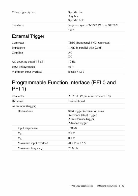
Video trigger types Specific lineAny lineSpecific field
Standards Negative sync of NTSC, PAL, or SECAMsignal
External TriggerConnector TRIG (front panel BNC connector)
Impedance 1 MΩ in parallel with 22 pF
Coupling ACDC
AC-coupling cutoff (-3 dB) 12 Hz
Input voltage range ±5 V
Maximum input overload |Peaks| ≤42 V
Programmable Function Interface (PFI 0 andPFI 1)Connector AUX I/O (9-pin mini-circular DIN)
Direction Bi-directional
As an input (trigger)
Destinations Start trigger (acquisition arm)Reference (stop) triggerArm reference triggerAdvance trigger
Input impedance 150 kΩ
VIH 2.0 V
VIL 0.8 V
Maximum input overload -0.5 V to 5.5 V
Maximum frequency 25 MHz
PXIe-5122 Specifications | © National Instruments | 15
As an output (event)
Sources Ready for StartStart trigger (acquisition arm)Ready for ReferenceReference (stop) triggerEnd of RecordReady for AdvanceAdvance triggerDone (end of acquisition)Probe Compensation26
Output impedance 50 Ω
Logic type 3.3 V CMOS
Maximum drive current ±12 mA
Maximum frequency 25 MHz
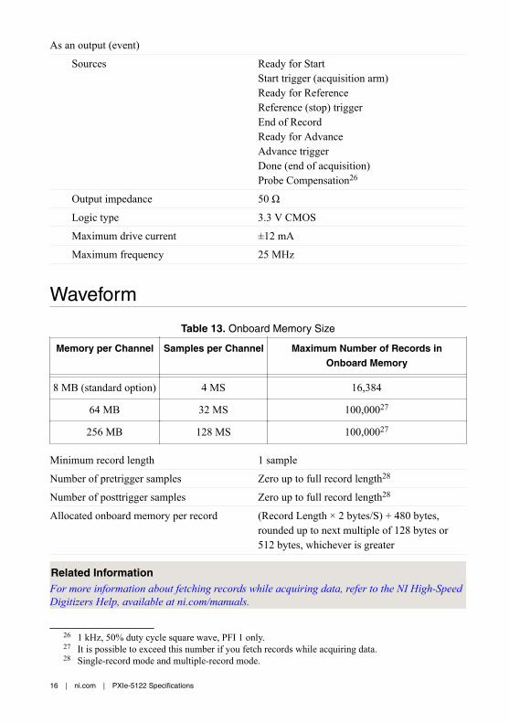
Waveform
Table 13. Onboard Memory Size
Memory per Channel Samples per Channel Maximum Number of Records inOnboard Memory
8 MB (standard option) 4 MS 16,384
64 MB 32 MS 100,00027
256 MB 128 MS 100,00027
Minimum record length 1 sample
Number of pretrigger samples Zero up to full record length28
Number of posttrigger samples Zero up to full record length28
Allocated onboard memory per record (Record Length × 2 bytes/S) + 480 bytes,rounded up to next multiple of 128 bytes or512 bytes, whichever is greater
Related InformationFor more information about fetching records while acquiring data, refer to the NI High-SpeedDigitizers Help, available at ni.com/manuals.
26 1 kHz, 50% duty cycle square wave, PFI 1 only.27 It is possible to exceed this number if you fetch records while acquiring data.28 Single-record mode and multiple-record mode.
16 | ni.com | PXIe-5122 Specifications
Calibration
External CalibrationExternal calibration calibrates the VCXO and the voltage reference. All calibration constantsare stored in nonvolatile memory.
Self-CalibrationSelf-calibration is done on software command. The calibration corrects for gain, offset,frequency response, triggering, and timing adjustment errors for all input ranges.
Calibration SpecificationsInterval for external calibration 2 years
Warm-up time 15 minutes
Software
Driver SoftwareDriver support for this device was first available in NI-SCOPE 3.3.1.
NI-SCOPE is an IVI-compliant driver that allows you to configure, control, and calibrate thePXIe-5122. NI-SCOPE provides application programming interfaces for many developmentenvironments.
Application SoftwareNI-SCOPE provides programming interfaces, documentation, and examples for the followingapplication development environments:• LabVIEW• LabWindows™/CVI™
• Measurement Studio• Microsoft Visual C/C++• .NET (C# and VB.NET)
Interactive Soft Front Panel and ConfigurationThe NI-SCOPE Soft Front Panel (SFP) allows interactive control of the PXIe-5122.
Interactive control of the PXIe-5122 was first available in NI-SCOPE SFP version 2.7. TheNI-SCOPE SFP is included on the NI-SCOPE media.
NI Measurement Automation Explorer (MAX) also provides interactive configuration and testtools for the PXIe-5122. MAX is included on the NI-SCOPE media.
PXIe-5122 Specifications | © National Instruments | 17
TClk SpecificationsYou can use the NI TClk synchronization method and the NI-TClk driver to align the Sampleclocks on any number of supported devices, in one or more chassis. For more informationabout TClk synchronization, refer to the NI-TClk Synchronization Help, which is locatedwithin the NI High-Speed Digitizers Help. For other configurations, including multichassissystems, contact NI Technical Support at ni.com/support.
Intermodule SMC Synchronization Using NI-TClk for IdenticalModulesSpecifications are valid under the following conditions:• PXI-5122 modules installed in one NI PXI-1042 chassis, or PXIe-5122 modules installed
in one PXI Express chassis.• All parameters set to identical values for each SMC-based module.• Sample clock set to 100 MS/s and all filters disabled.
Note Although you can use NI-TClk to synchronize non-identical modules, thesespecifications apply only to synchronizing identical modules.
Skew29 500 ps, typical
Average skew after manual adjustment30 <10 ps, typical
Sample clock delay/adjustment resolution ≤10 ps, typical
PowerCurrent draw
+3.3 VDC 1.6 A, typical1.6 A, maximum
+12 VDC 2.0 A, typical2.32 A, maximum
Total power 29.28 W, typical33.12 W, maximum
29 Caused by clock and analog path delay differences. No manual adjustment performed.30 For information about manual adjustment, refer to the Synchronization Repeatability Optimization
topic in the NI-TClk Synchronization Help available at ni.com/manuals. For additional help withthe adjustment process, contact NI Technical Support at ni.com/support.
18 | ni.com | PXIe-5122 Specifications
Dimensions and WeightDimensions 3U, one-slot, PXI Express module
21.3 cm × 2.0 cm × 13.0 cm(8.4 in × 0.8 in × 5.1 in)
Weight 453 g (16.0 oz)
EnvironmentMaximum altitude 2,000 m (800 mbar) (at 25 °C ambient
temperature)
Pollution Degree 2
Indoor use only.
Operating EnvironmentNote Refer to KnowledgeBase 4AEB2ML1 at ni.com for information aboutmaximizing PXI Express data transfer rates when operating at ambient temperaturesbelow 10 °C.
Ambient temperature range 0 °C to 55 °C (Tested in accordance withIEC 60068-2-1 and IEC 60068-2-2. MeetsMIL-PRF-28800F Class 3 low temperaturelimit and MIL-PRF-28800F Class 2 hightemperature limit.)
Relative humidity range 10% to 90%, noncondensing (Tested inaccordance with IEC 60068-2-56.)
Storage EnvironmentAmbient temperature range -40 °C to 71 °C (Tested in accordance
with IEC 60068-2-1 and IEC 60068-2-2. MeetsMIL-PRF-28800F Class 3 limits.)
Relative humidity range 5% to 95%, noncondensing (Tested inaccordance with IEC 60068-2-56.)
PXIe-5122 Specifications | © National Instruments | 19
Shock and VibrationOperating shock 30 g peak, half-sine, 11 ms pulse (Tested in
accordance with IEC 60068-2-27. MeetsMIL-PRF-28800F Class 2 limits.)
Storage shock 50 g peak, half-sine, 11 ms pulse (MeetsIEC 60068-2-27. Test profile developed inaccordance with MIL-PRF-28800F.)
Random vibration
Operating 5 Hz to 500 Hz, 0.3 grms (Tested in accordancewith IEC 60068-2-64.)
Nonoperating 5 Hz to 500 Hz, 2.4 grms (Tested in accordancewith IEC 60068-2-64. Test profile exceeds therequirements of MIL-PRF-28800F, Class 3.)
Compliance and Certifications
SafetyThis product is designed to meet the requirements of the following electrical equipment safetystandards for measurement, control, and laboratory use:• IEC 61010-1, EN 61010-1• UL 61010-1, CSA C22.2 No. 61010-1
Note For UL and other safety certifications, refer to the product label or the OnlineProduct Certification section.
Electromagnetic CompatibilityThis product meets the requirements of the following EMC standards for electrical equipmentfor measurement, control, and laboratory use:• EN 61326-1 (IEC 61326-1): Class A emissions; Basic immunity• EN 55011 (CISPR 11): Group 1, Class A emissions• EN 55022 (CISPR 22): Class A emissions• EN 55024 (CISPR 24): Immunity• AS/NZS CISPR 11: Group 1, Class A emissions• AS/NZS CISPR 22: Class A emissions
20 | ni.com | PXIe-5122 Specifications
• FCC 47 CFR Part 15B: Class A emissions• ICES-001: Class A emissions
Note In the United States (per FCC 47 CFR), Class A equipment is intended foruse in commercial, light-industrial, and heavy-industrial locations. In Europe,Canada, Australia, and New Zealand (per CISPR 11), Class A equipment is intendedfor use only in heavy-industrial locations.
Note Group 1 equipment (per CISPR 11) is any industrial, scientific, or medicalequipment that does not intentionally generate radio frequency energy for thetreatment of material or inspection/analysis purposes.
Note For EMC declarations, certifications, and additional information, refer to the Online Product Certification section.
CE Compliance This product meets the essential requirements of applicable European Directives, as follows:• 2014/35/EU; Low-Voltage Directive (safety)• 2014/30/EU; Electromagnetic Compatibility Directive (EMC)
Online Product CertificationRefer to the product Declaration of Conformity (DoC) for additional regulatory complianceinformation. To obtain product certifications and the DoC for this product, visit ni.com/certification, search by model number or product line, and click the appropriate link in theCertification column.
Environmental ManagementNI is committed to designing and manufacturing products in an environmentally responsiblemanner. NI recognizes that eliminating certain hazardous substances from our products isbeneficial to the environment and to NI customers.
For additional environmental information, refer to the Minimize Our Environmental Impactweb page at ni.com/environment. This page contains the environmental regulations anddirectives with which NI complies, as well as other environmental information not included inthis document.
Waste Electrical and Electronic Equipment (WEEE)EU Customers At the end of the product life cycle, all NI products must bedisposed of according to local laws and regulations. For more information abouthow to recycle NI products in your region, visit ni.com/environment/weee.
电子信息产品污染控制管理办法(中国 RoHS)中国客户 National Instruments 符合中国电子信息产品中限制使用某些有害物
质指令(RoHS)。关于 National Instruments 中国 RoHS 合规性信息,请登录
PXIe-5122 Specifications | © National Instruments | 21
ni.com/environment/rohs_china。(For information about China RoHScompliance, go to ni.com/environment/rohs_china.)
Information is subject to change without notice. Refer to the NI Trademarks and Logo Guidelines at ni.com/trademarks forinformation on NI trademarks. Other product and company names mentioned herein are trademarks or trade names of theirrespective companies. For patents covering NI products/technology, refer to the appropriate location: Help»Patents in yoursoftware, the patents.txt file on your media, or the National Instruments Patent Notice at ni.com/patents. You can findinformation about end-user license agreements (EULAs) and third-party legal notices in the readme file for your NI product. Referto the Export Compliance Information at ni.com/legal/export-compliance for the NI global trade compliance policy and howto obtain relevant HTS codes, ECCNs, and other import/export data. NI MAKES NO EXPRESS OR IMPLIED WARRANTIES ASTO THE ACCURACY OF THE INFORMATION CONTAINED HEREIN AND SHALL NOT BE LIABLE FOR ANY ERRORS. U.S.Government Customers: The data contained in this manual was developed at private expense and is subject to the applicablelimited rights and restricted data rights as set forth in FAR 52.227-14, DFAR 252.227-7014, and DFAR 252.227-7015.
© 2003—2017 National Instruments. All rights reserved.
376938C-01 December 12, 2017


![Ç o v^ ] } v · î ô &ODVV](https://static.fdocument.org/doc/165x107/621c22aaeca1c872404f6486/-o-v-v-ampodvv.jpg)


![CHARAKTERYSTYKI STAŁOPRĄDOWE … · dsp =β p V in −V DD −V tp] 2 [( ) 2 1 2 out dsn n in tn out V I =βV −V V ...](https://static.fdocument.org/doc/165x107/5b96032409d3f2d7438d1c5c/charakterystyki-stalopradowe-dsp-p-v-in-v-dd-v-tp-2-2-1-2.jpg)