P-N Junctions/Diodes - Department of Electrical and ...rlake/EE203/ee612_Taur2.pdf · (b) qψ bi...
42
P-N Junctions/Diodes p n V I V log I slope = 60 mV/decade V I
Transcript of P-N Junctions/Diodes - Department of Electrical and ...rlake/EE203/ee612_Taur2.pdf · (b) qψ bi...
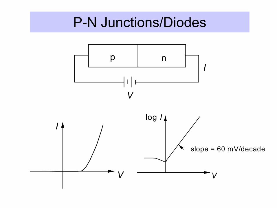
P-N Junctions/Diodes
p n
V
I
V
log I
slope = 60 mV/decade
V
I
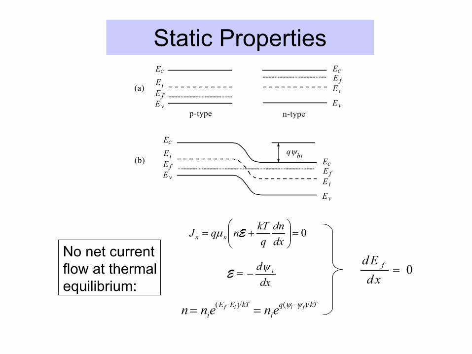
Static Properties
(b)qψbi
(a)
cE
Ev
EiE f
n-typep-type
cE
Ev
Ei
E f
cE
Ev
EiE f cE
Ev
Ei
E f
0=
+=
dxdn
qkTnqJ nn Eµ
dxd= iψ
−E
n n e n eiE E kT
iq kTf i i f= =− −( )/ ( )/ψ ψ
d Ed x
f = 0No net current flow at thermal equilibrium:
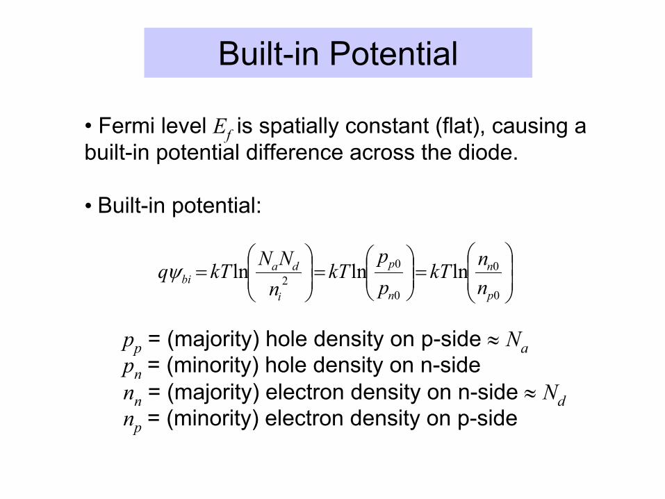
Built-in Potential
• Fermi level Ef is spatially constant (flat), causing a built-in potential difference across the diode.
• Built-in potential:
pp = (majority) hole density on p-side ≈ Napn = (minority) hole density on n-sidenn = (majority) electron density on n-side ≈ Ndnp = (minority) electron density on p-side
=
=
=
0
0
0
02 lnlnln
p
n
n
p
i
dabi n
nkTpp
kTnNNkTqψ
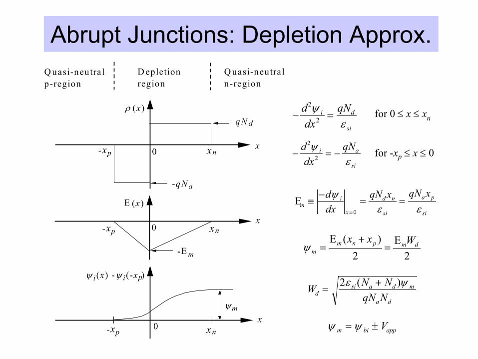
Abrupt Junctions: Depletion Approx.
0 xxn-xp
ρ (x)
x
E (x)
-E m
xψm
qN d
a-qN
Q uasi-neutralp-region
Q uasi-neutraln-region
D epletion region
-xp xn
xn-xp
0
0
pψ (x) -ψ (-x )i i
Emi
x
d n
si
a p
si
ddx
qN x qN x≡
−= =
=
ψε ε0
− =ddx
qNi d
si
2
2ψ
ε
− = −ddx
qNi a
si
2
2ψ
ε
for 0 ≤ x ≤ xn
for -xp ≤ x ≤ 0
W N NqN Nd
si a d m
a d
=+2ε ψ( )
ψ ψm bi appV= ±
2E
2)(E dmpnm
mWxx
=+
=ψ
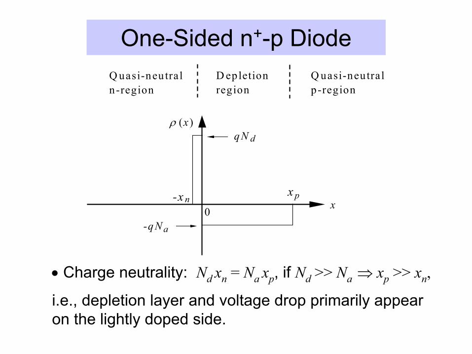
One-Sided n+-p Diode
0 x-x n
x p
ρ (x )qN d
a-qN
Q uasi-neu traln-region
Q uasi-neutralp-region
D epletion region
• Charge neutrality: Nd xn = Na xp, if Nd >> Na ⇒ xp >> xn,
i.e., depletion layer and voltage drop primarily appear on the lightly doped side.

One-Sided n+-p Diode• Built-in potential:
1E+14 1E+15 1E+16 1E+17 1E+180.70
0.75
0.80
0.85
0.90
0.95
1.00
1.05Bu
ilt-in
pot
entia
l (V
)
Doping concentration (cm−3)
+≈
i
agbi n
NkTE
q ln2
ψ
⇒ Built-in potential a weak function of doping conc.
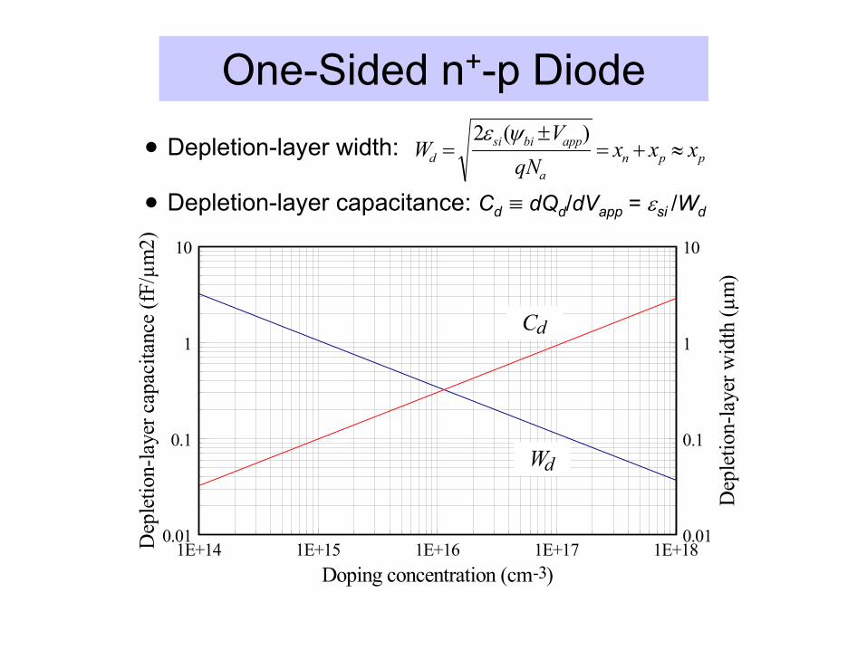
One-Sided n+-p Diode• Depletion-layer width:
• Depletion-layer capacitance: Cd ≡ dQd/dVapp = εsi /Wd
1E+14 1E+15 1E+16 1E+17 1E+180.01
0.1
1
10
0.01
0.1
1
10
Doping concentration (cm )
Dep
letio
n-la
yer c
apac
itanc
e (f
F/µm
2)
Dep
letio
n-la
yer w
idth
(µm
)
Cd
Wd
-3
ppna
appbisid xxx
qNV
W ≈+=±
=)(2 ψε
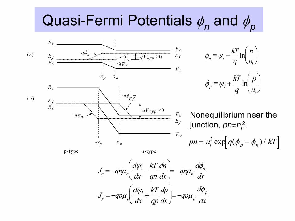
Quasi-Fermi Potentials φn and φp
cE
E v
E f(a) -qφn
-qφp
n-typep-type
qV <0app
(b)
-qφn
-qφp
cE
E v
E f qV >0app
cE
E v
E f
x n
x n
-xp
-xp
cE
E v
E f
[ ]pn n q kTi p n= −2 exp ( ) /φ φ
φ ψn ii
kTq
nn
≡ −
ln
φ ψp ii
kTq
pn
≡ +
ln
J qnddx
kTqn
dndx
qnddxn n
in
n= − −
= −µ
ψµ
φ
J qpddx
kTqp
dpdx
qpddxp p
ip
p= − +
= −µ
ψµ
φ
Nonequilibrium near the junction, pn≠ni
2.

Spatial Variations of φn and φp
cE
E v
E f(a) -qφn
-qφp
n-typep-type
qV <0app
(b)
-qφn
-qφp
cE
E v
E f qV >0app
cE
E v
E f
x n
x n
-xp
-xp
cE
E v
E f
Vapp = φp − φn at junction boundaries.
Inside the space-charge region: Jn is constant (neglect G-R currents)
⇒ [nnµndφn/dx]xn = [npµndφn/dx]−xp
⇒ [dφn/dx at xn] << [dφn/dx at −xp]
⇒φn ~ constant inside space-charge region
Practically all spatial variation in φn occurs in p-region,
Likewise, all spatial variation in φp occurs in n-region.

Spatial Variations of φn and φp
cE
E v
E f(a) -qφn
-qφp
n-typep-type
qV <0app
(b)
-qφn
-qφp
cE
E v
E f qV >0app
cE
E v
E f
x n
x n
-xp
-xp
cE
E v
E f
Vapp = φp − φn at junction boundaries.
pn = ni2exp[q(φp − φn)/kT]
Vapp > 0 for forward bias,Vapp < 0 for reverse bias.
(1) np(x = −xp) ≈ np0(x = −xp) exp(qVapp/kT ) (2) pn(x = xn) ≈ pn0(x = xn) exp(qVapp/kT )
(1) and (2) are the most important boundary conditions governing a p-n diode.
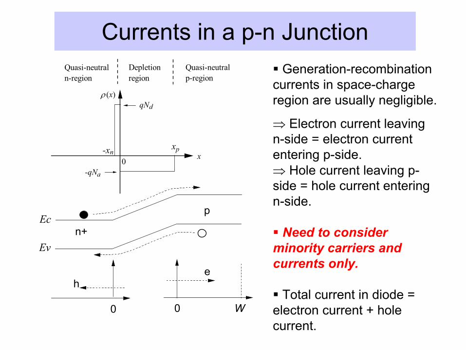
Currents in a p-n Junction
0 x-xn
xp
ρ (x)qN d
a-qN
Quasi-neutraln-region
Quasi-neutralp-region
Depletion region
Ec
Ev
0 W0
eh
n+
p
Generation-recombination currents in space-charge region are usually negligible.
⇒ Electron current leaving n-side = electron current entering p-side.⇒ Hole current leaving p-side = hole current entering n-side.
Need to consider minority carriers and currents only.
Total current in diode = electron current + hole current.

Excess Electrons in the p-Region
W/L = 0.2
0.5 1.0 2.0
exp(-x/L)
0 0.5 1 1.5 2 2.5 30
0.2
0.4
0.6
0.8
1
x/L
Nom
aliz
ed e
xces
s ele
ctro
n de
nsity
01=+−= nn
n GRxJ
qtn
∂∂
∂∂
dxdnkT
dxdn
qnkT
dxdqnJ nnn µψµ =
−−=
nnn
nnGRτ
0−=−
L DkT
qn n nn n≡ =τ
µ τd ndx
n nL
p p p
n
2
20
2 0−−
= , where is the
minority carrier diffusion length.
Boundary conditions:
at x=0, and
at x=W (ohmic contact).
( )n n qV kTp p app= 0 exp /
n np p= 0
[ ] [ ]n n n qV kTW x L
W Lp p p appn
n
− = −−
0 0 1exp( / )sinh ( ) /
sinh( / ).
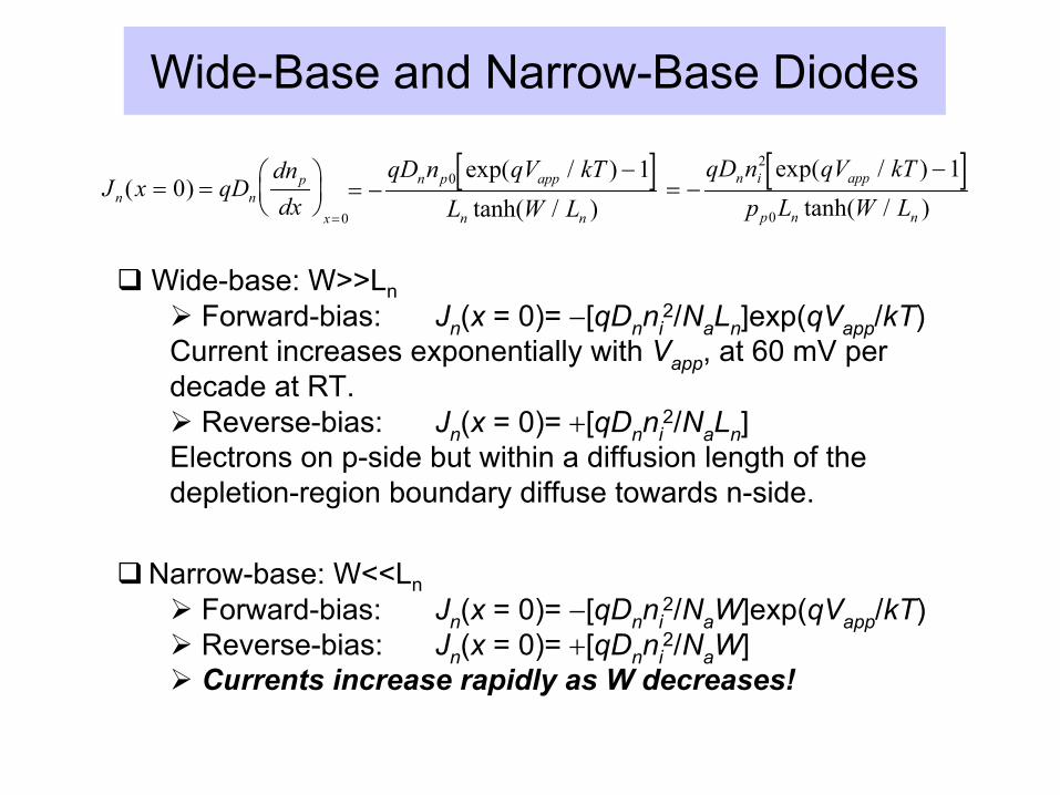
Wide-Base and Narrow-Base Diodes
J x qDdndxn n
p
x
( )= =
=
00
[ ]= −
−qD n qV kTL W L
n p app
n n
0 1exp( / )tanh( / )
[ ]= −
−qD n qV kTp L W L
n i app
p n n
2
0
1exp( / )tanh( / )
Wide-base: W>>LnForward-bias: Jn(x = 0)= −[qDnni
2/NaLn]exp(qVapp/kT)Current increases exponentially with Vapp, at 60 mV per decade at RT.
Reverse-bias: Jn(x = 0)= +[qDnni2/NaLn]
Electrons on p-side but within a diffusion length of the depletion-region boundary diffuse towards n-side.
Narrow-base: W<<LnForward-bias: Jn(x = 0)= −[qDnni
2/NaW]exp(qVapp/kT)Reverse-bias: Jn(x = 0)= +[qDnni
2/NaW]Currents increase rapidly as W decreases!
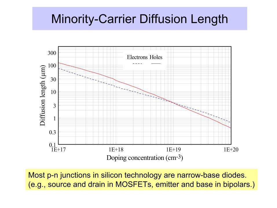
Minority-Carrier Diffusion Length
1E+17 1E+18 1E+19 1E+200.1
0.3
1
3
10
30
100
300
Doping concentration (cm )
Diff
usio
n le
ngth
(µm
)
Electrons Holes
-3
Most p-n junctions in silicon technology are narrow-base diodes.(e.g., source and drain in MOSFETs, emitter and base in bipolars.)

Turning Off a p-n Diode
Excess electrons in p-region
Effective turn off starts only after most excess minority carriers have recombined or have drained off.
t ts
i(t)IF
-IR
0
t = 0
t > 0
t = ts
x
(n - n )p0p
0
t < 0n+ p
VF R i(t)
VR
n+ p
R i(t)
t > 0
x0
Q q n n dxB
W
p p= − −∫ ( )0 0
1E+17 1E+18 1E+19 1E+201E-10
1E-9
1E-8
1E-7
1E-6
1E-5
1E-4
Doping concentration (cm )
Min
ority
-car
rier l
ifetim
e (s
) Electrons Holes
-3

Diffusion Capacitance
Diffusion capacitance CD is due to stored minority carriers responding to applied voltage.
CD due to electrons stored in p-type region:
CDn = dQB/dVapp ∝ exp(qVapp/kT)
For a diode or bipolar transistor to switch fast, it must have minimal diffusion capacitance.
To minimize diffusion capacitance: increase doping concentration and minimize charge-storage volume.
Modern high-speed bipolar transistors require very thin base.
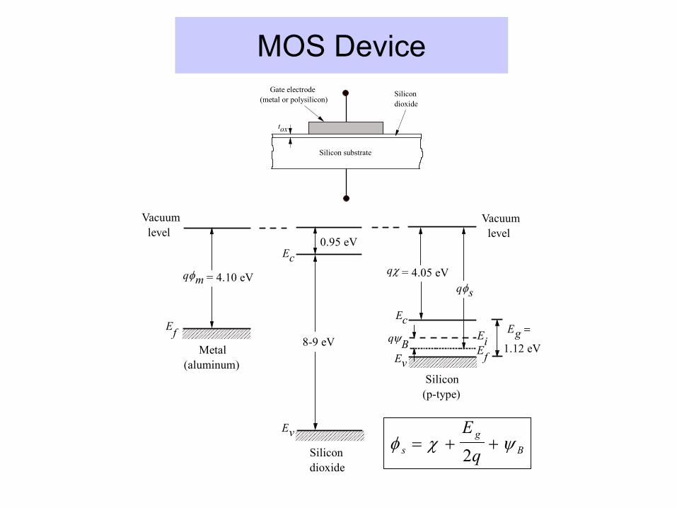
MOS Device
Vacuum level
Vacuum level
Ec
Ec
Ev
Ev
= 4.10 eV
0.95 eV
8-9 eV
= 4.05 eVqχq mφq sφ
Metal(aluminum)
Silicondioxide
Silicon(p-type)
1.12 eV
Eg =q Bψ Ei
Ef
Ef
Silicon dioxide
Gate electrode(metal or polysilicon)
Silicon substrate
tox
φ χ ψsg
B
Eq
= + +2
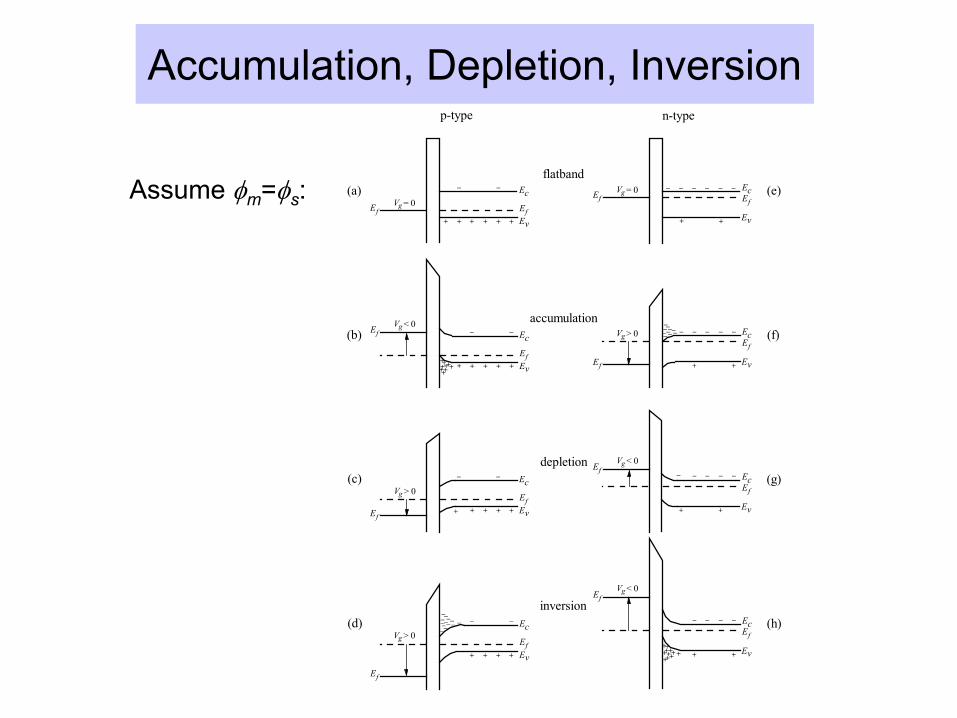
Accumulation, Depletion, Inversion
(a)
(b)
(c)
(d) (h)
(g)
(f)
(e)Ec
Ev
Ef
Ef
V = 0g
Ec
Ev
Ef
Ef
Ec
Ev
Ef
Ef
V = 0g
Ec
Ev
Ef Ef
p-type n-type
flatband
accumulation
depletion
inversion
V < 0g V > 0g
Ec
Ev
Ef Ef
V > 0g
Ec
Ev
Ef
Ef
V < 0g
Ec
Ev
Ef
Ef
V > 0g
Ec
Ev
Ef
Ef
V < 0g
+ + + + + +
+ + + + + +
+ +
_ _ _ __ __ _
_ __ __
+ +
_ _ __ ______ __
++++ ++ ++
+ + + + +
_ _ _ __ __
+ +
+ + + +
__ __
+ +
_ ____ __ ___ _____
++ +++++ +++
+
Assume φm=φs:
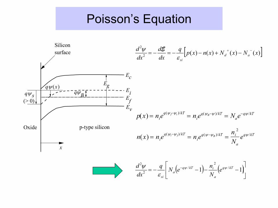
Poisson’s Equation
q sψ(> 0)
Ec
Ei
Ev
Egq Bψ
Oxide p-type silicon
x
Siliconsurface
q xψ ( )
Ef
[ ])()()()(2
2
xNxNxnxpqdxd
dxd
adsi
−+ −+−−=−=ε
ψ E
( ) ( )
−−−−= − 11 /
2/
2
2kTq
a
ikTqa
si
eNneNq
dxd ψψ
εψ
p x n e n e N eiq kT
iq kT
aq kTf i B( ) ( )/ ( )/ /= = =− − −ψ ψ ψ ψ ψ
n x n e n enN
eiq kT
iq kT i
a
q kTi f B( ) ( )/ ( )/ /= = =− −ψ ψ ψ ψ ψ2
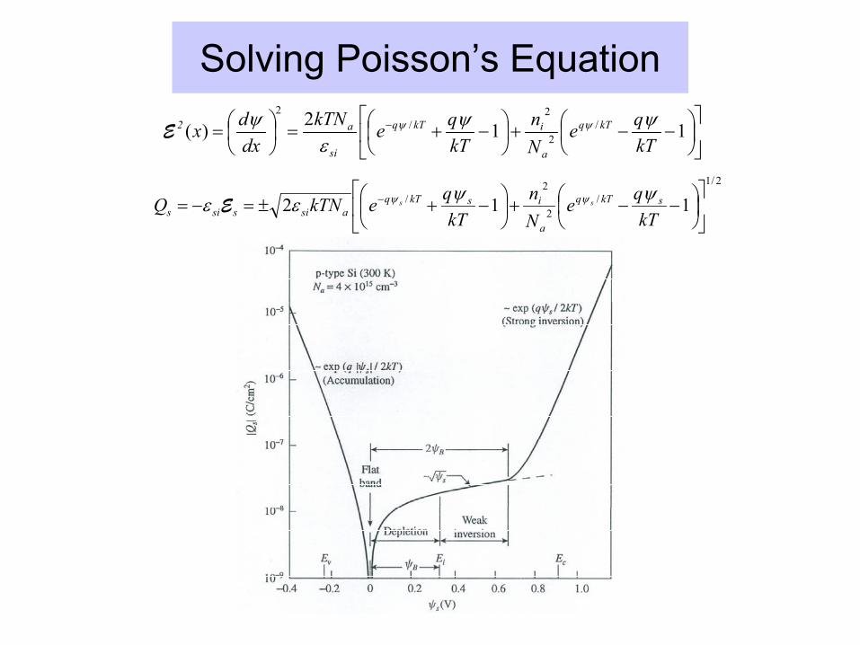
Solving Poisson’s Equation
−−+
−+=
= − 112)( /
2
2/
2
kTqe
Nn
kTqekTN
dxdx kTq
a
ikTq
si
a2 ψψε
ψ ψψE
2/1
/2
2/ 112
−−+
−+±=−= −
kTqe
Nn
kTqekTNQ skTq
a
iskTqasissis
ssψψεε ψψE
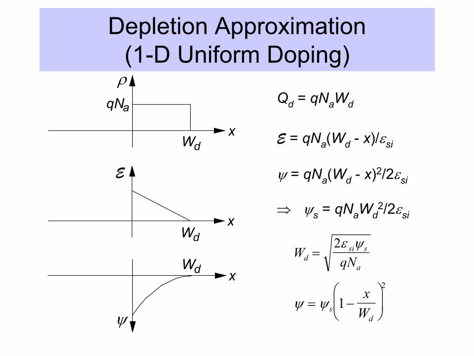
Depletion Approximation(1-D Uniform Doping)
Wdx
qNa
ρ
xWd
E
xWd
ψ
E
Qd = qNaWd
E = qNa(Wd - x)/εsi
ψ = qNa(Wd - x)2/2εsi
⇒ ψs = qNaWd2/2εsi
WqNd
si s
a=
2ε ψ
ψ ψ= −
s
d
xW
12

Condition for Strong Inversion
q sψ(> 0)
Ec
Ei
Ev
Egq Bψ
Oxide p-type silicon
x
Siliconsurface
q xψ ( )
Ef
ψ ψs Ba
iinv
kTq
Nn
( ) ln= =
2 2
i.e., (ni2/Na
2)exp(qψs/kT) = 1.
And the electron concentration at the surface equals the hole concentration in the bulkSi.
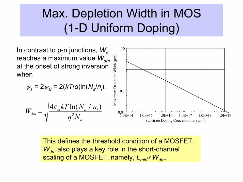
Max. Depletion Width in MOS(1-D Uniform Doping)
W kT N nq Ndm
si a i
a
=4
2ε ln( / )
In contrast to p-n junctions, Wdreaches a maximum value Wdmat the onset of strong inversion when
ψs = 2ψB = 2(kT/q)ln(Na/ni):
This defines the threshold condition of a MOSFET.Wdm also plays a key role in the short-channel scaling of a MOSFET, namely, Lmin∝Wdm.
1.0E+14 1.0E+15 1.0E+16 1.0E+17 1.0E+18 1.0E+190.01
0.1
1
10
Substrate Doping Concentration (cm )M
axim
um D
eple
tion
Wid
th (µ
m)
-3

Strong Inversion
ddx
kTN qkT
nN
ea
si
i
a
q kTψε
ψ ψ= − +
2 2
2/
0 50 100 150 2000
2E+18
4E+18
6E+18
8E+18
1E+19
1.2E+19
Na = −1016 3 cm
ψ s = 088. V
ψ s = 085. V
Distance from surface, x ( )Å
Elec
tron
conc
entra
tion,
n(x
) (c
m
)-3 Charge per area:
Electron conc. at surface:
Inversion layer thickness: Qi/qn(0) = 2εsikT/qQi
QkTnN
eisi i
a
q kTs= −2 2
2ε ψ /
nnN
ei
a
q kTs( ) /02
= ψ
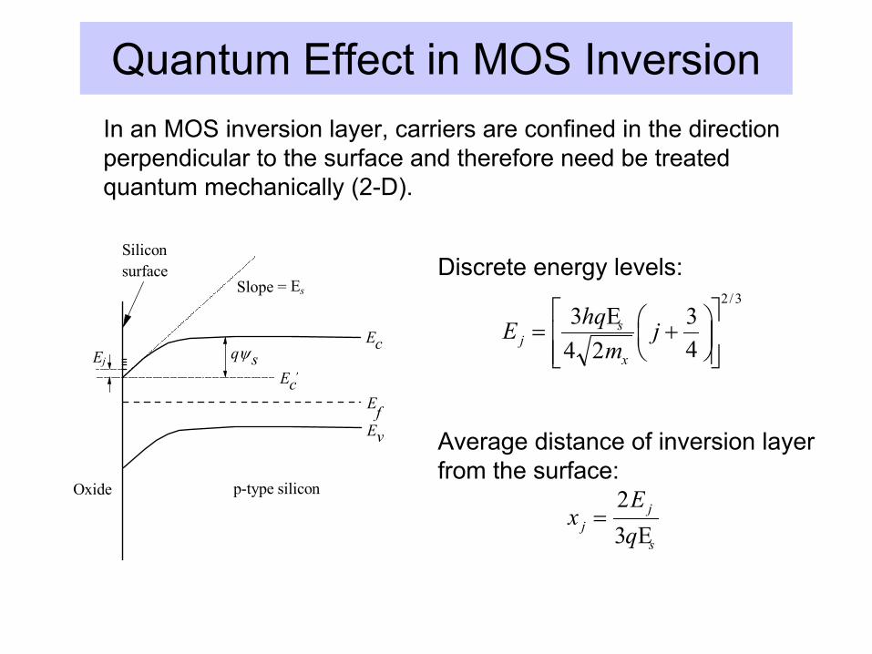
Quantum Effect in MOS Inversion
q sψEc
Ev
Oxide p-type silicon
Siliconsurface
Ej
Slope = Es
Ec′
Ef
In an MOS inversion layer, carriers are confined in the direction perpendicular to the surface and therefore need be treated quantum mechanically (2-D).
E hqm
jjs
x
= +
34 2
34
2 3E
/
xEqj
j
s
=23 E
Discrete energy levels:
Average distance of inversion layer from the surface:

Self-Consistent QM SolutionEl
ectro
n en
ergy
Conductionband edge
Bottom of the well
Lowest subband
Oxi
deEl
ectro
n de
nsity
Classical
Quantum
Depth
Electron ground state isat some finite energy above the bottom of theconduction band.
Band bending mustexceed 2ψB to invertsurface.
The centroid of inversionlayer is farther awayfrom the surface than inthe classical case.
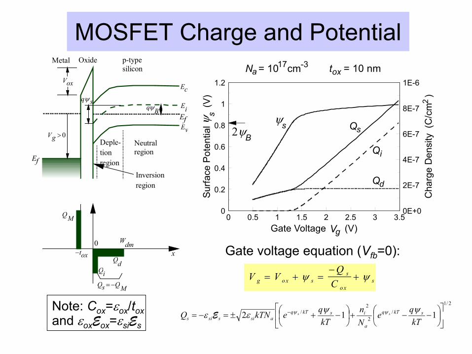
MOSFET Charge and Potential
0 0.5 1 1.5 2 2.5 3 3.50
0.2
0.4
0.6
0.8
1
1.2
0E+0
2E-7
4E-7
6E-7
8E-7
1E-6
Gate Voltage (V)
Surfa
ce P
oten
tial
(
V)
Cha
rge
Den
sity
(C
/cm
)
t = 10 nmoxN = 10 cma17 -3
Vg
ψsψ s
2
Qs
Qd
Qi
2ψB
Oxide p-type silicon
q sψ
Ec
Ei
Ev
q Bψ
Metal
Vg > 0
Vox
QM
QdQi
0
Qs QM= −
x
Deple-tionregion
Inversionregion
Neutral region
−tox
Wdm
Ef
Ef
Gate voltage equation (Vfb=0):
V VQ
Cg o x ss
o xs= + =
−+ψ ψ
Note: Cox=εox/toxand εoxEox=εsiEs
2/1
/2
2/ 112
−−+
−+±=−= −
kTqe
Nn
kTqekTNQ skTq
a
iskTqasissis
ssψψεε ψψE
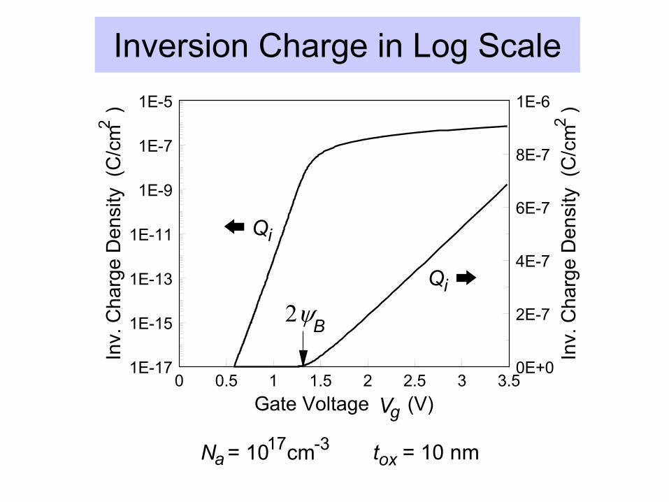
Inversion Charge in Log Scale
0 0.5 1 1.5 2 2.5 3 3.51E-17
1E-15
1E-13
1E-11
1E-9
1E-7
1E-5
0E+0
2E-7
4E-7
6E-7
8E-7
1E-6
Gate Voltage (V)
Inv.
Cha
rge
Den
sity
(C
/cm
)
Inv.
Cha
rge
Den
sity
(C
/cm
)
t = 10 nmoxN = 10 cma17 -3
Vg
2
Qi
2ψB
2
Qi
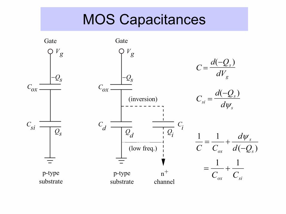
MOS Capacitances
Csi Ci
Cox
Gate
p-typesubstrate
(low freq.)
(inversion)
n+channel
Cd
Cox
Gate
p-typesubstrate
Vg Vg
−Qs −Qs
Qs Qd Qi
Cd Q
dVs
g=
−( )
Cd Q
dsis
s=
−( )ψ
)(11
s
s
ox Qdd
CC −+=
ψ
siox CC11
+=

Capacitance-Voltage Characteristics
In accumulation, Qs∝exp(-qψs/2kT), so Csi=-dQs/dψs=(q/2kT)Qs=(q/2kT)Cox|Vg-ψs|.
1 1
12
C CkT q
Vox g s
= +−
/ψ
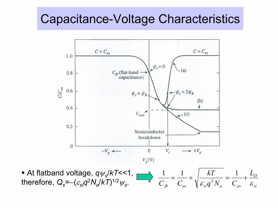
Capacitance-Voltage Characteristics
At flatband voltage, qψs/kT<<1, therefore, Qs=−(εsiq2Na/kT)1/2ψs. si
D
oxasioxfb
LCNq
kTCC εε
+=+=111 2
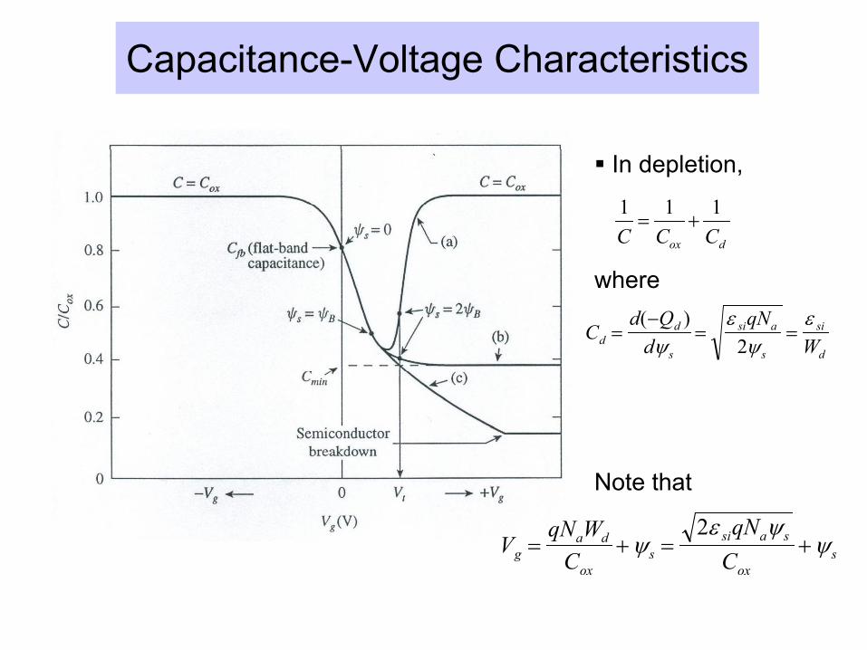
Capacitance-Voltage Characteristics
In depletion,
where
Note that
Cd Q
dqN
Wdd
s
si a
s
si
d=
−= =
( )ψ
εψ
ε2
VqN W
CqN
Cga d
oxs
si a s
oxs= + = +ψ
ε ψψ
2
dox CCC111 +=
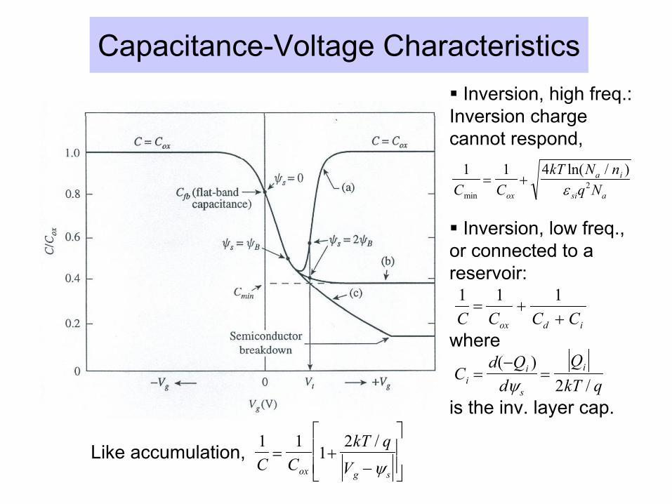
Capacitance-Voltage CharacteristicsInversion, high freq.:
Inversion charge cannot respond,
Inversion, low freq., or connected to a reservoir:
where
is the inv. layer cap.
1 1 4
2C CkT N n
q Nox
a i
si amin
ln( / )= +
ε
1 1 1C C C Cox d i
= ++
Cd Q
dQ
kT qii
s
i=−
=( )
/ψ 2
1 1
12
C CkT q
Vox g s
= +−
/ψ
Like accumulation,

Split C-V Measurement
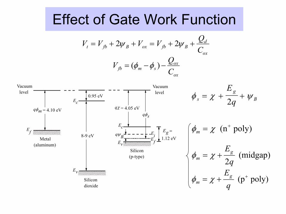
Effect of Gate Work Function V V V V Q
Ct fb B ox fb Bd
ox
= + + = + +2 2ψ ψ
Vacuum level
Vacuum level
Ec
Ec
Ev
Ev
= 4.10 eV
0.95 eV
8-9 eV
= 4.05 eVqχq mφq sφ
Metal(aluminum)
Silicondioxide
Silicon(p-type)
1.12 eV
Eg =q Bψ Ei
Ef
Ef
ox
oxsmfb C
QV −−= )( φφ
φ χ ψsg
B
Eq
= + +2
poly) (n += χφm
poly) (p ++=q
Egm χφ
(midgap) 2qEg
m += χφ
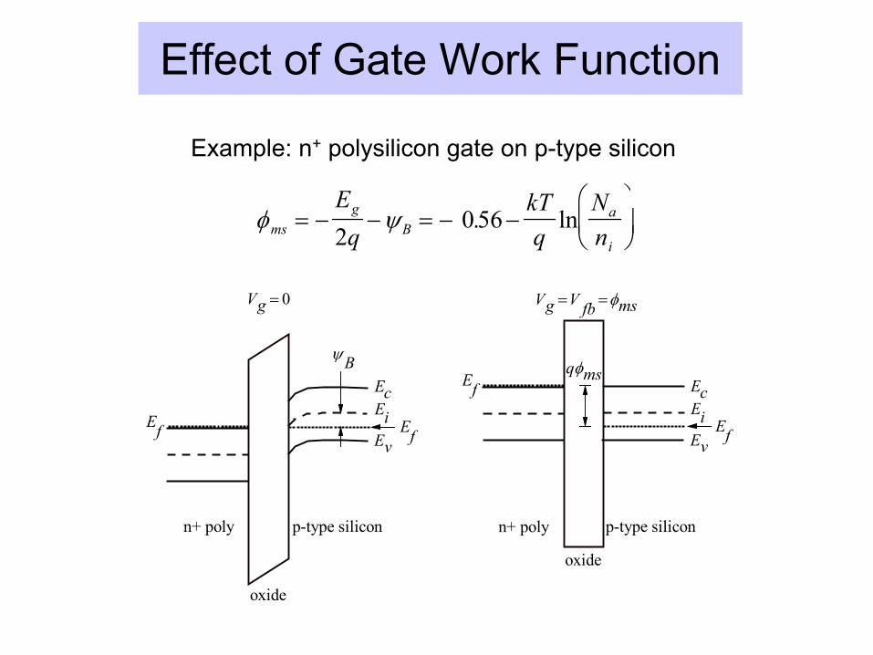
Effect of Gate Work Function
oxide
p-type siliconn+ poly
q msφ
Vg V fb ms= =φ
n+ poly
oxide
p-type silicon
Vg = 0
Ec
Ev
Ei
Ec
Ev
Ei
ψB
Ef
Ef
Ef Ef
Example: n+ polysilicon gate on p-type silicon
φ ψmsg
Ba
i
Eq
kTq
Nn
= − − = − −
2
0 56. ln

Poly-Si Gate Depletion Effect
Ec
Ei
Ev
Vox
Ec
Ei
Ev
Vg
p-type siliconOxiden+ poly
ψp
ψs
Ef
Ef
V VQCg fb s p
s
ox= + + −ψ ψ
1 1 1 1C C C Cox si p
= + +
Gate eq. becomes:
and,
-2 -1 0 1 20
0.2
0.4
0.6
0.8
1
Cinv
Typically, tinv is 0.8-1.0 nm thicker than tox.

Gated-Diode: MOS + p-n JunctionZero-bias on the p-n junction (equilibrium):
The electron quasi-Fermi level in the MOS is the same as the Fermi level of the p-type Si.⇒ Inversion occurs when ψs = 2ψB.

Gated-Diode: Reverse Biased (Nonequilibrium)
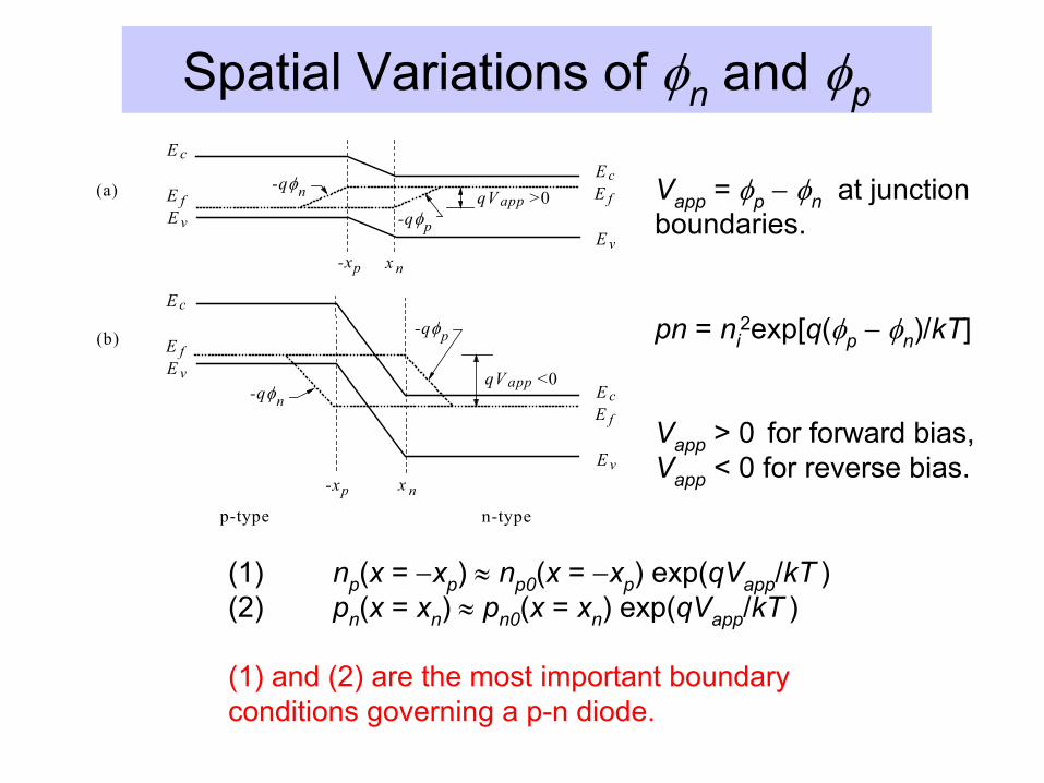
Spatial Variations of φn and φp
cE
E v
E f(a) -qφn
-qφp
n-typep-type
qV <0app
(b)
-qφn
-qφp
cE
E v
E f qV >0app
cE
E v
E f
x n
x n
-xp
-xp
cE
E v
E f
Vapp = φp − φn at junction boundaries.
pn = ni2exp[q(φp − φn)/kT]
Vapp > 0 for forward bias,Vapp < 0 for reverse bias.
(1) np(x = −xp) ≈ np0(x = −xp) exp(qVapp/kT ) (2) pn(x = xn) ≈ pn0(x = xn) exp(qVapp/kT )
(1) and (2) are the most important boundary conditions governing a p-n diode.

MOS under Nonequilibrium
For a p-n junction reverse-biased at a voltage VR, the electron concentration on the p-side of the junction is
If a gate voltage is applied to bend the p-type bands by ψs, the electron concentration at the surface is
For surface inversion to occur, i.e., n = Na,Need
nnN
ei
a
qV kTR= −2
/
n nN
e ei
a
q kT qV kTs R= −2
ψ / /
ψ ψs R Binv V( ) = + 2
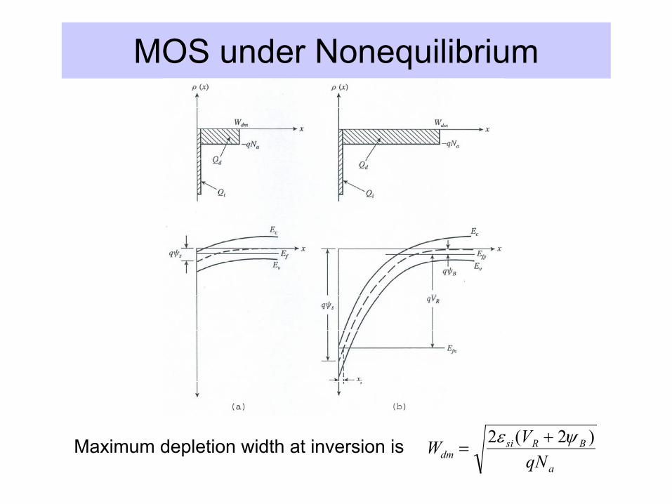
MOS under Nonequilibrium
W VqNdm
si R B
a
=+2 2ε ψ( )Maximum depletion width at inversion is