Monolithic Bi-Directional Switches X -Technology of 3 ΦAC ...
29
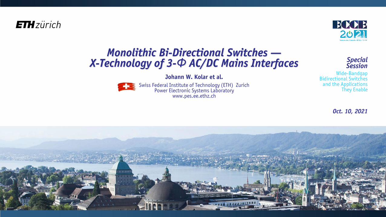
Oct. 10, 2021 Special Session Wide-Bandgap Bidirectional Switches and the Applications They Enable Monolithic Bi - Directional Switches — X - Technology of 3 - Φ AC/DC Mains Interfaces Johann W. Kolar et al. Swiss Federal Institute of Technology (ETH) Zurich Power Electronic Systems Laboratory www.pes.ee.ethz.ch
Transcript of Monolithic Bi-Directional Switches X -Technology of 3 ΦAC ...
/16
Oct. 10, 2021
SpecialSession
Wide-Bandgap Bidirectional Switches
and the Applications They Enable
Monolithic Bi-Directional Switches —X-Technology of 3-Φ AC/DC Mains Interfaces
Johann W. Kolar et al.Swiss Federal Institute of Technology (ETH) Zurich
Power Electronic Systems Laboratorywww.pes.ee.ethz.ch
/16
Oct. 10, 2021
Johann W. Kolar | Jonas E. Huber | F. Vollmaier | Daifei Zhang | Neha NainSwiss Federal Institute of Technology (ETH) Zurich
Power Electronic Systems Laboratorywww.pes.ee.ethz.ch
SpecialSession
Wide-Bandgap Bidirectional Switches
and the Applications They Enable
M-BDS — X-Technology of 3-Φ AC/DC Mains Interfaces
/16
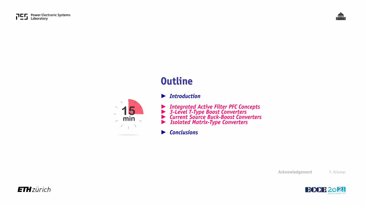
Outline► Introduction
► Integrated Active Filter PFC Concepts ► 3-Level T-Type Boost Converters► Current Source Buck-Boost Converters► IIsolated Matrix-Type Converters
► Conclusions
Acknowledgement F. Krismer
/16
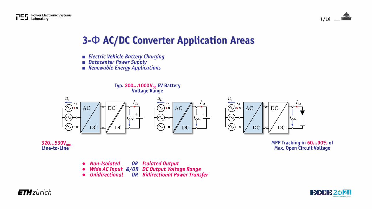
3-Φ AC/DC Converter Application Areas ■ Electric Vehicle Battery Charging■ Datacenter Power Supply ■ Renewable Energy Applications
● Non-Isolated OR Isolated Output● Wide AC Input &/OR DC Output Voltage Range● Unidirectional OR Bidirectional Power Transfer
320…530VrmsLine-to-Line
Typ. 200…1000VDC EV Battery Voltage Range
MPP Tracking in 60…90% of Max. Open Circuit Voltage
1
/16
SiC/GaN Semiconductors Multi-Cell/Level ConceptsFunctional IntegrationSynergetic Association3D-Packaging/IntegrationMLCC & HF Mag. MaterialsDigitalization / IIoT
■ Power Electronics 1.0 Power Electronics 4.0■ Driven by Key Technologies / “X-Concepts”
S-Curve of Power Electronics
Power MOSFETs & IGBTsCircuit Topologies
MicroelectronicsModulation Concepts
Control Concepts
Super-Junct. Techn. / WBGDigital Power
Modeling & Simulation
20252015
►
►►
SCRs / Diodes Solid-State Devices
■
►
►
1958
4.0
3.0
2.0
1.0
2
►
►
►
►
/16
3rd Harmonic Injection PFC Rectifier
/16
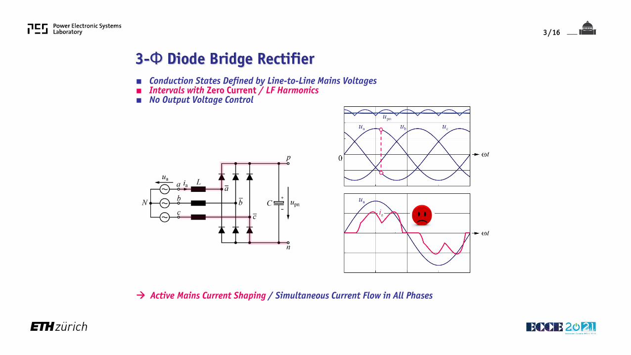
3-Φ Diode Bridge Rectifier■ Conduction States Defined by Line-to-Line Mains Voltages ■ Intervals with Zero Current / LF Harmonics■ No Output Voltage Control
Active Mains Current Shaping / Simultaneous Current Flow in All Phases
3
/16
● Non-Sinusoidal Mains Current
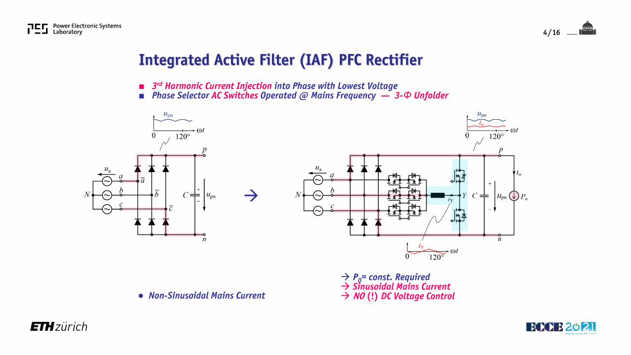
PO= const. Required Sinusoidal Mains Current NO (!) DC Voltage Control
■ 3rd Harmonic Current Injection into Phase with Lowest Voltage ■ Phase Selector AC Switches Operated @ Mains Frequency — 3-Φ Unfolder
Integrated Active Filter (IAF) PFC Rectifier
4
/16
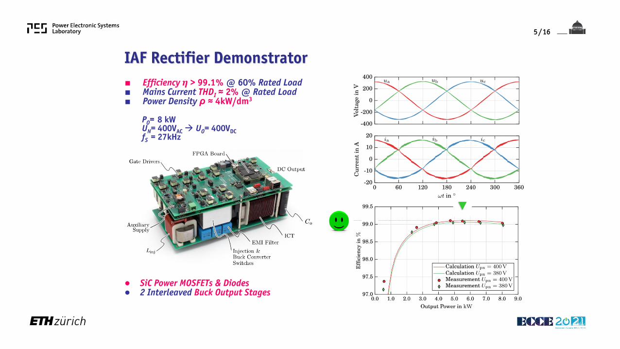
IAF Rectifier Demonstrator■ Efficiency η > 99.1% @ 60% Rated Load■ Mains Current THDI ≈ 2% @ Rated Load■ Power Density ρ ≈ 4kW/dm3
● SiC Power MOSFETs & Diodes● 2 Interleaved Buck Output Stages
PO= 8 kWUN= 400VAC UO= 400VDCfS = 27kHz
►
5
/16
Source:
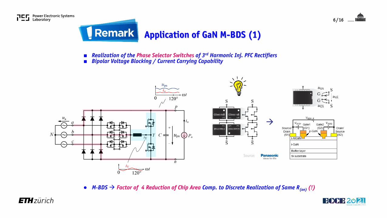
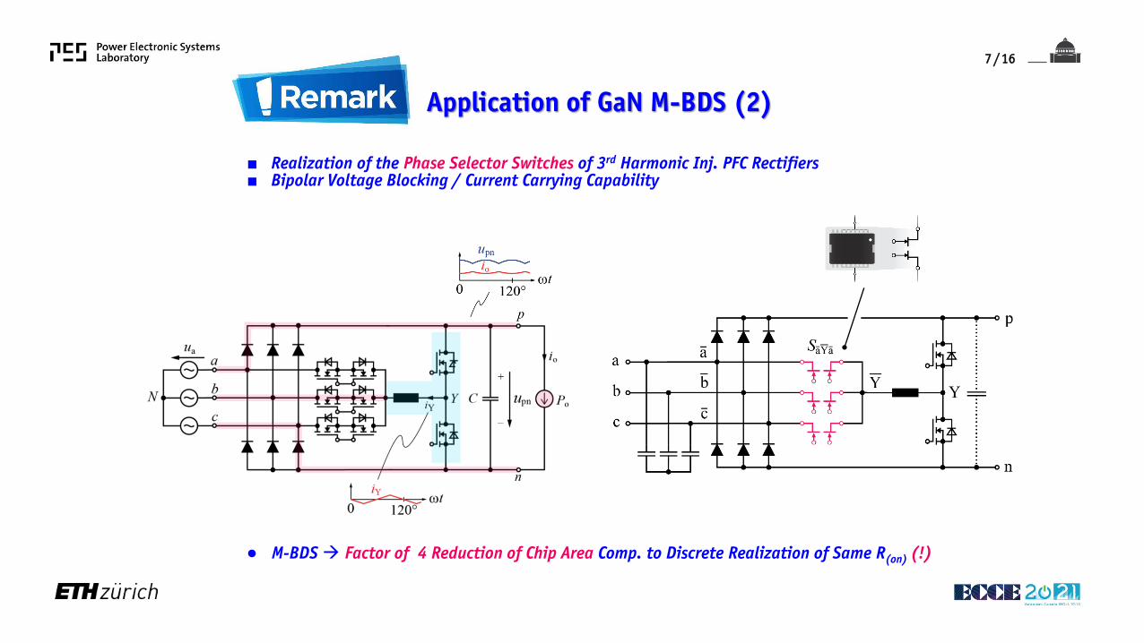
■ Realization of the Phase Selector Switches of 3rd Harmonic Inj. PFC Rectifiers■ Bipolar Voltage Blocking / Current Carrying Capability
6
Application of GaN M-BDS (1)
● M-BDS Factor of 4 Reduction of Chip Area Comp. to Discrete Realization of Same R(on) (!)
/167
Application of GaN M-BDS (2)
■ Realization of the Phase Selector Switches of 3rd Harmonic Inj. PFC Rectifiers■ Bipolar Voltage Blocking / Current Carrying Capability
● M-BDS Factor of 4 Reduction of Chip Area Comp. to Discrete Realization of Same R(on) (!)
/16
3-Level T-Type PFC Rectifier
/16
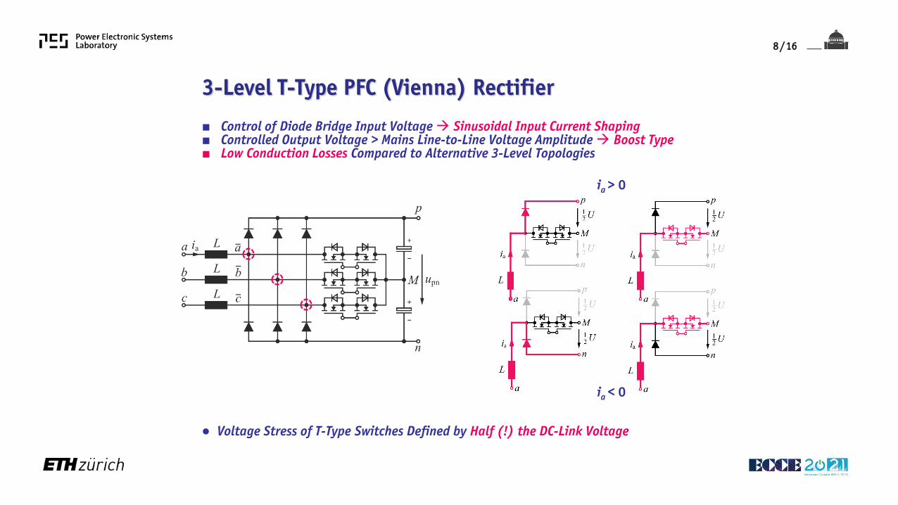
■ Control of Diode Bridge Input Voltage Sinusoidal Input Current Shaping■ Controlled Output Voltage > Mains Line-to-Line Voltage Amplitude Boost Type■ Low Conduction Losses Compared to Alternative 3-Level Topologies
● Voltage Stress of T-Type Switches Defined by Half (!) the DC-Link Voltage
8
3-Level T-Type PFC (Vienna) Rectifier
ia > 0
ia < 0
/16
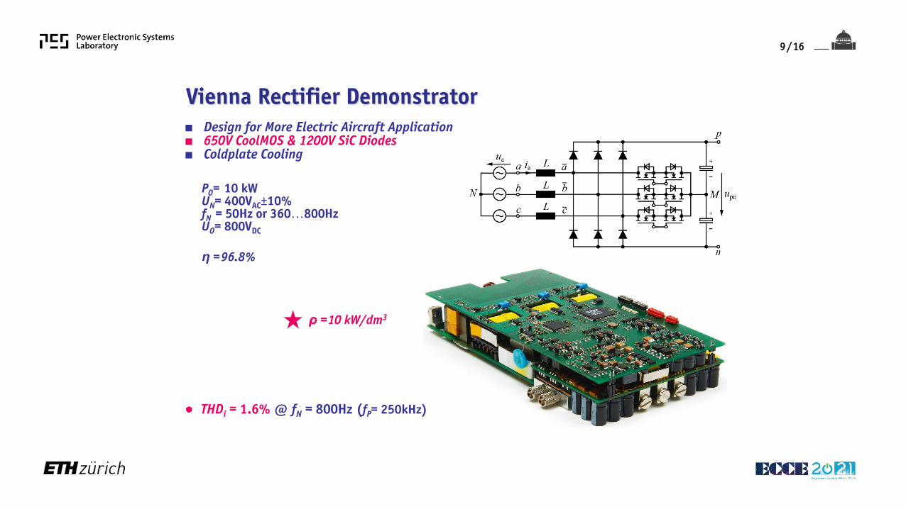
PO= 10 kWUN= 400VAC±10%fN = 50Hz or 360…800HzUO= 800VDC
ρ =10 kW/dm3
■ Design for More Electric Aircraft Application■ 650V CoolMOS & 1200V SiC Diodes■ Coldplate Cooling
● THDi = 1.6% @ fN = 800Hz (fP= 250kHz)
η =96.8%
Vienna Rectifier Demonstrator
9
/16
Application of GaN M-BDS
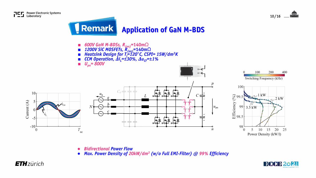
■ 600V GaN M-BDSs, R(on)=140mΩ■ 1200V SiC MOSFETs, R(on)=140mΩ■ Heatsink Design for Tj=120°C, CSPI= 15W/dm3K■ CCM Operation, ΔiL=±30%, ΔuCF=±1%■ Upn= 800V
● Bidirectional Power Flow● Max. Power Density of 20kW/dm3 (w/o Full EMI-Filter) @ 99% Efficiency
10
/16
Buck-Boost Current DC-Link
PFC Rectifier
/16
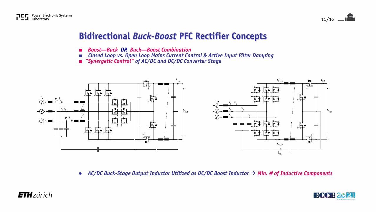
● AC/DC Buck-Stage Output Inductor Utilized as DC/DC Boost Inductor Min. # of Inductive Components
■ Boost—Buck OR Buck—Boost Combination■ Closed Loop vs. Open Loop Mains Current Control & Active Input Filter Damping ■ “Synergetic Control” of AC/DC and DC/DC Converter Stage
Bidirectional Buck-Boost PFC Rectifier Concepts
11
/16
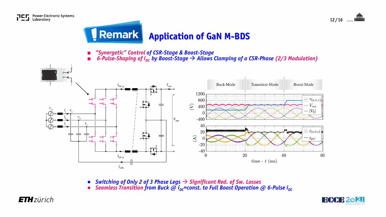
● Switching of Only 2 of 3 Phase Legs Significant Red. of Sw. Losses ● Seamless Transition from Buck @ iDC=const. to Full Boost Operation @ 6-Pulse iDC
12
Application of GaN M-BDS
■ “Synergetic” Control of CSR-Stage & Boost-Stage ■ 6-Pulse-Shaping of iDC by Boost-Stage Allows Clamping of a CSR-Phase (2/3 Modulation)
/16
3-Φ Isolated Matrix-Type PFC
Rectifier
/16
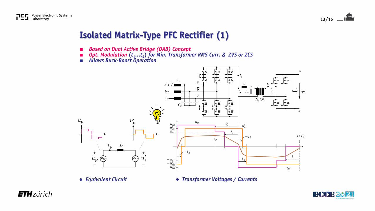
■ Based on Dual Active Bridge (DAB) Concept■ Opt. Modulation (t1…t4) for Min. Transformer RMS Curr. & ZVS or ZCS■ Allows Buck-Boost Operation
● Equivalent Circuit ● Transformer Voltages / Currents
Isolated Matrix-Type PFC Rectifier (1)
13
/16
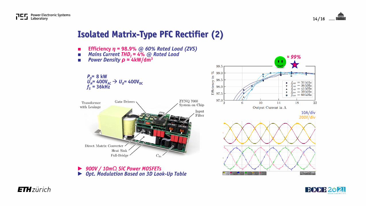
► 900V / 10mΩ SiC Power MOSFETs ► Opt. Modulation Based on 3D Look-Up Table
PO= 8 kWUN= 400VAC UO= 400VDCfS = 36kHz
■ Efficiency η = 98.9% @ 60% Rated Load (ZVS)■ Mains Current THDI ≈ 4% @ Rated Load ■ Power Density ρ ≈ 4kW/dm3
10A/div200V/div
≈ 99%
Isolated Matrix-Type PFC Rectifier (2)
14
/16
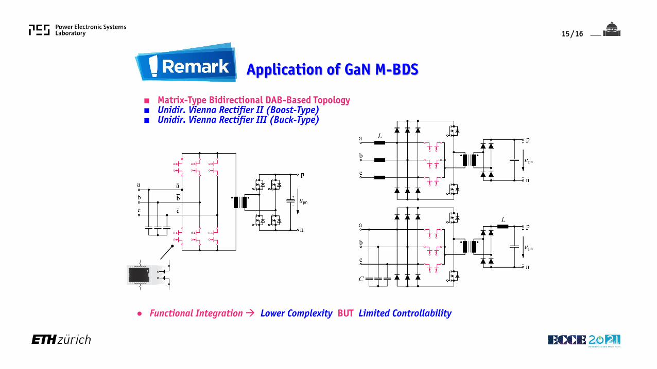
● Functional Integration Lower Complexity BUT Limited Controllability
■ Matrix-Type Bidirectional DAB-Based Topology ■ Unidir. Vienna Rectifier II (Boost-Type)■ Unidir. Vienna Rectifier III (Buck-Type)
15
Application of GaN M-BDS
/16
Outlook
/16
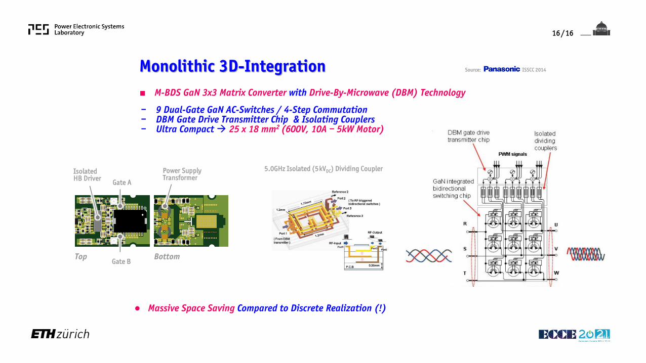
Monolithic 3D-Integration ■ M-BDS GaN 3x3 Matrix Converter with Drive-By-Microwave (DBM) Technology
– 9 Dual-Gate GaN AC-Switches / 4-Step Commutation– DBM Gate Drive Transmitter Chip & Isolating Couplers– Ultra Compact 25 x 18 mm2 (600V, 10A – 5kW Motor)
Source: ISSCC 2014
5.0GHz Isolated (5kVDC) Dividing Coupler
16
● Massive Space Saving Compared to Discrete Realization (!)
Top Bottom
Isolated HB Driver Gate A
Gate B
Power Supply Transformer
/16
Thank you!
/16
/16B-1
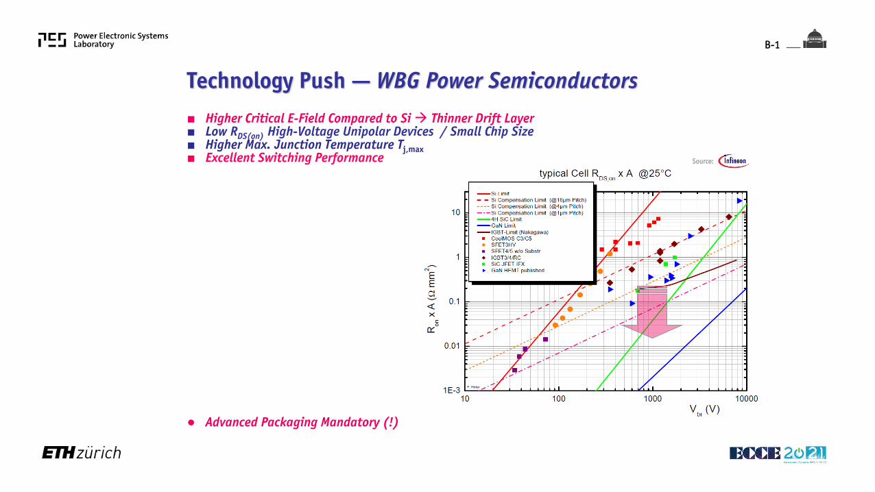
Source:
● Advanced Packaging Mandatory (!)
Technology Push — WBG Power Semiconductors■ Higher Critical E-Field Compared to Si Thinner Drift Layer■ Low RDS(on) High-Voltage Unipolar Devices / Small Chip Size■ Higher Max. Junction Temperature Tj,max■ Excellent Switching Performance
/16
Technology Push — Digitalization
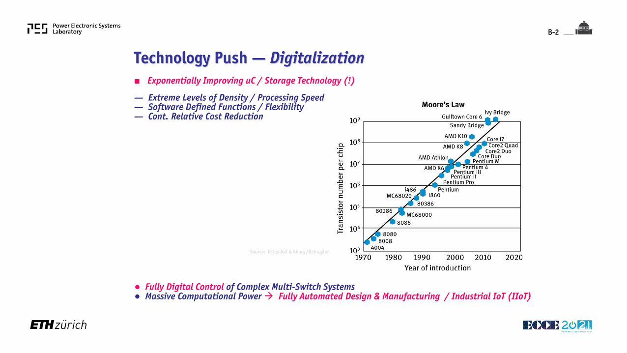
● Fully Digital Control of Complex Multi-Switch Systems● Massive Computational Power Fully Automated Design & Manufacturing / Industrial IoT (IIoT)
Source: Ostendorf & König /DeGruyter
■ Exponentially Improving uC / Storage Technology (!)
— Extreme Levels of Density / Processing Speed— Software Defined Functions / Flexibility — Cont. Relative Cost Reduction
B-2
/16
End