Allosteric signaling Biochemistry Direct negative feedback Indirect feedback Cyclic processes.
Data Sheet
Co
mlin
ear CLC1606 1.3GH
z Current Feedback Am
plifier Rev 1D
Comlinear® CLC1606
1.3GHz Current Feedback Amplifier
Exar Corporation www.exar.com48720 Kato Road, Fremont CA 94538, USA Tel. +1 510 668-7000 - Fax. +1 510 668-7001
F E A T U R E Sn 1.2GHz -3dB bandwidth at G=2 n 3,300V/μs slew raten 0.01%/0.01˚ differential gain/ phase errorn 7.5mA supply currentn 875MHz large signal bandwidthn 120mA output current (easily drives three video loads)n Fully specified at 5V and ±5V suppliesn CLC1606: Pb-free SOT23-5n CLC1606: Pb-free SOIC-8
A P P L I C A T I O N Sn RGB video line driversn High definition video drivern Video switchers and routersn ADC buffern Active filtersn High-speed instrumentationn Wide dynamic range IF amp
General Description
The COMLINEAR CLC1606 is a high-performance, current feedback amplifier with superior bandwith and video specifications. The CLC1606 provides 1.3GHz unity gain bandwidth, ±0.1dB gain flatness to 150MHz, and provides 3,300V/μs slew rate exceeding the requirements of high-definition television (HDTV) and other multimedia applications. The COMLINEAR CLC1606 high-performance amplifier also provide ample output current to drive multiple video loads.
The COMLINEAR CLC1606 is designed to operate from ±5V or +5V supplies. It consumes only 7.5mA of supply current. The combination of high-speed and excellent video performance make the CLC1606 well suited for use in many general purpose, high-speed applications including standard definition and high definition video. Data communications applications benefit from the CLC1606’s total harmonic distortion of -68dBc at 10MHz and fast settling time to 0.1%.
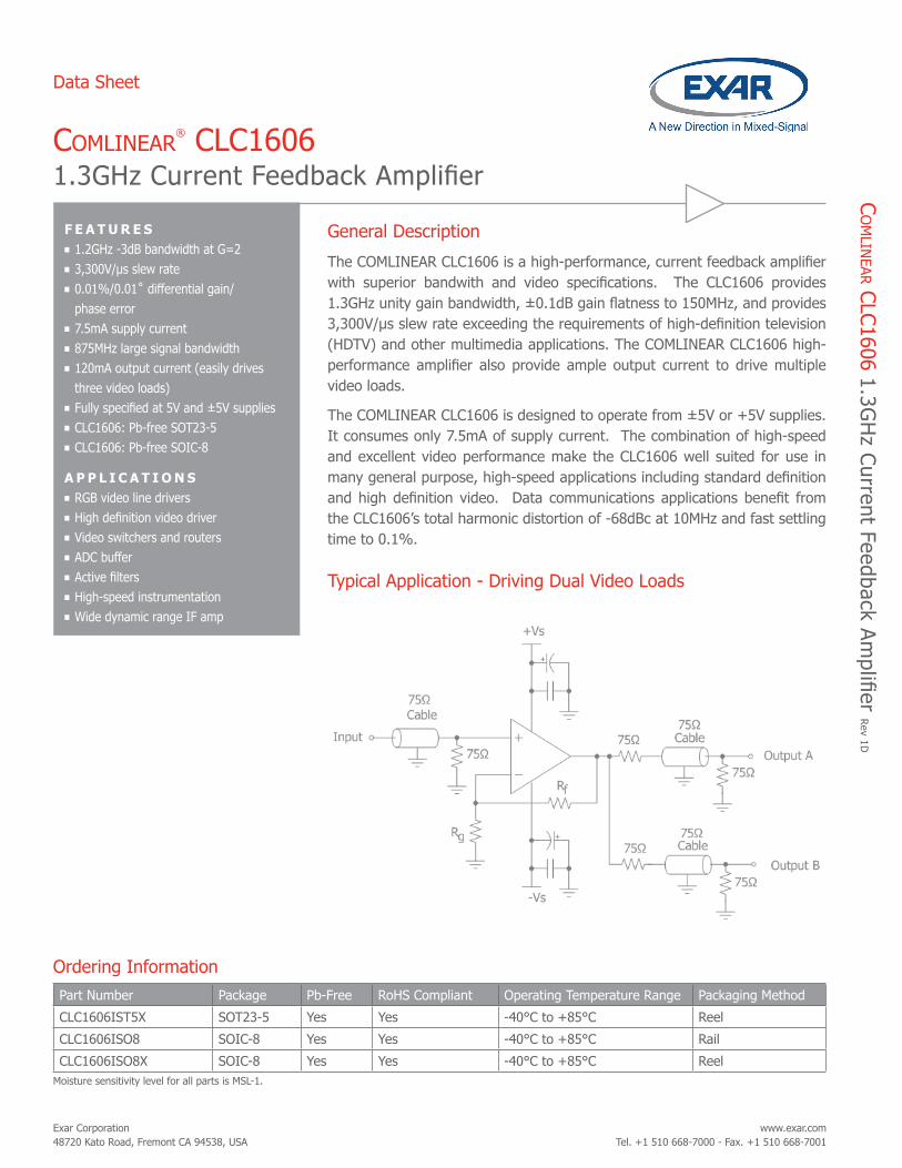
Typical Application - Driving Dual Video Loads
Ordering InformationPart Number Package Pb-Free RoHS Compliant Operating Temperature Range Packaging Method
CLC1606IST5X SOT23-5 Yes Yes -40°C to +85°C Reel
CLC1606ISO8 SOIC-8 Yes Yes -40°C to +85°C Rail
CLC1606ISO8X SOIC-8 Yes Yes -40°C to +85°C ReelMoisture sensitivity level for all parts is MSL-1.
Data SheetC
om
linear CLC1606 1.3G
Hz C
urrent Feedback Amplifier R
ev 1D
©2007-2013 Exar Corporation 2/18 Rev 1D
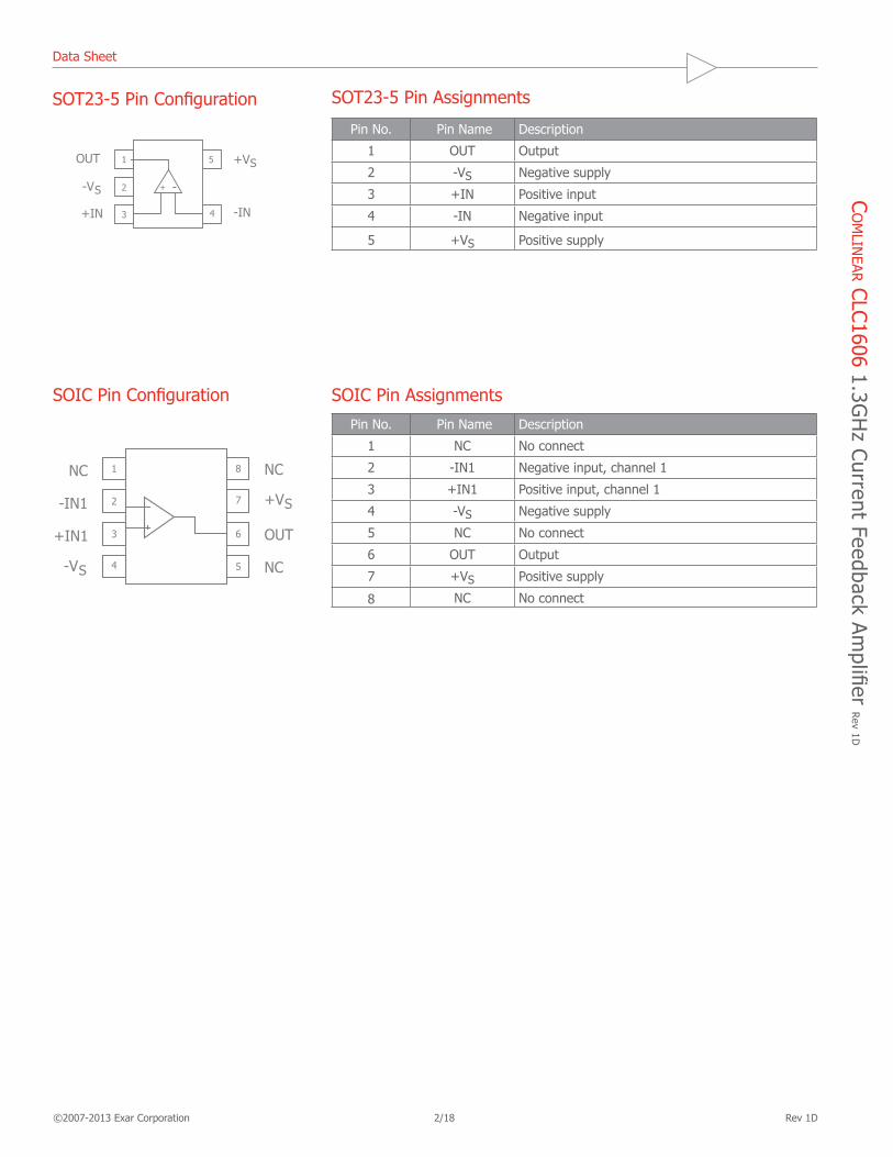
SOT23-5 Pin Assignments
Pin No. Pin Name Description
1 OUT Output
2 -VS Negative supply
3 +IN Positive input
4 -IN Negative input
5 +VS Positive supply
SOT23-5 Pin Configuration
2
3
5
4+IN
+VS
-IN
1
-VS
OUT
-+
SOIC Pin Assignments
Pin No. Pin Name Description
1 NC No connect
2 -IN1 Negative input, channel 1
3 +IN1 Positive input, channel 1
4 -VS Negative supply
5 NC No connect
6 OUT Output
7 +VS Positive supply
8 NC No connect
SOIC Pin Configuration
2
3
4 5
6
7
8
+IN1
NC
OUT
NC
1
-IN1
NC
-VS
+VS

Data SheetC
om
linear CLC1606 1.3G
Hz C
urrent Feedback Amplifier R
ev 1D
©2007-2013 Exar Corporation 3/18 Rev 1D
Absolute Maximum Ratings
The safety of the device is not guaranteed when it is operated above the “Absolute Maximum Ratings”. The device should not be operated at these “absolute” limits. Adhere to the “Recommended Operating Conditions” for proper de-vice function. The information contained in the Electrical Characteristics tables and Typical Performance plots reflect the operating conditions noted on the tables and plots.
Parameter Min Max Unit
Supply Voltage 0 14 VInput Voltage Range -Vs -0.5V +Vs +0.5V VContinuous Output Current 120 mA
Reliability InformationParameter Min Typ Max Unit
Junction Temperature 150 °CStorage Temperature Range -65 150 °CLead Temperature (Soldering, 10s) 260 °CPackage Thermal Resistance5-Lead SOT23 221 °C/W8-Lead SOIC 100 °C/W
Notes: Package thermal resistance (qJA), JDEC standard, multi-layer test boards, still air.
ESD ProtectionProduct SOT23-5
Human Body Model (HBM) (1) 2kVCharged Device Model (CDM) 1kV
Notes: 1. 0.8kV between the input pairs +IN and -IN pins only. All other pins are 2kV.
Recommended Operating ConditionsParameter Min Typ Max Unit
Operating Temperature Range -40 +85 °CSupply Voltage Range 4.5 12 V
Data SheetC
om
linear CLC1606 1.3G
Hz C
urrent Feedback Amplifier R
ev 1D
©2007-2013 Exar Corporation 4/18 Rev 1D
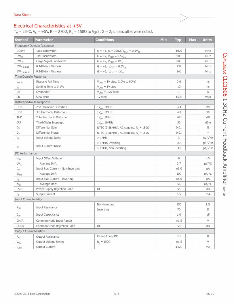
Electrical Characteristics at +5VTA = 25°C, Vs = +5V, Rf = 270Ω, RL = 150Ω to VS/2, G = 2; unless otherwise noted.
Symbol Parameter Conditions Min Typ Max Units
Frequency Domain Response
UGBW -3dB Bandwidth G = +1, Rf = 390Ω, VOUT = 0.5Vpp 1000 MHz
BWSS -3dB Bandwidth G = +2, VOUT = 0.5Vpp 900 MHz
BWLS Large Signal Bandwidth G = +2, VOUT = 1Vpp 800 MHz
BW0.1dBSS 0.1dB Gain Flatness G = +2, VOUT = 0.5Vpp 132 MHz
BW0.1dBLS 0.1dB Gain Flatness G = +2, VOUT = 1Vpp 140 MHz
Time Domain Response
tR, tF Rise and Fall Time VOUT = 1V step; (10% to 90%) 0.6 ns
tS Settling Time to 0.1% VOUT = 1V step 10 ns
OS Overshoot VOUT = 0.2V step 1 %
SR Slew Rate 1V step 1500 V/µs
Distortion/Noise Response
HD2 2nd Harmonic Distortion 1Vpp, 5MHz -74 dBc
HD3 3rd Harmonic Distortion 1Vpp, 5MHz -70 dBc
THD Total Harmonic Distortion 1Vpp, 5MHz 68 dB
IP3 Third-Order Intercept 1Vpp, 10MHz 36 dBm
DG Differential Gain NTSC (3.58MHz), AC-coupled, RL = 150Ω 0.01 %
DP Differential Phase NTSC (3.58MHz), AC-coupled, RL = 150Ω 0.01 °
en Input Voltage Noise > 1MHz 3 nV/√Hz
ini Input Current Noise> 1MHz, Inverting 20 pA/√Hz
> 1MHz, Non-inverting 30 pA/√Hz
DC Performance
VIO Input Offset Voltage 0 mV
dVIO Average Drift 3.7 µV/°C
Ibn Input Bias Current - Non-Inverting ±3.0 µA
dIbn Average Drift 100 nA/°C
Ibi Input Bias Current - Inverting ±6.0 µA
dIbi Average Drift 56 nA/°C
PSRR Power Supply Rejection Ratio DC 55 dB
IS Supply Current 6.5 mA
Input Characteristics
RIN Input ResistanceNon-inverting 150 kΩ
Inverting 70 Ω
CIN Input Capacitance 1.0 pF
CMIR Common Mode Input Range ±1.5 V
CMRR Common Mode Rejection Ratio DC 50 dB
Output Characteristics
RO Output Resistance Closed Loop, DC 0.1 Ω
VOUT Output Voltage Swing RL = 150Ω ±1.5 V
IOUT Output Current ±120 mA

Data SheetC
om
linear CLC1606 1.3G
Hz C
urrent Feedback Amplifier R
ev 1D
©2007-2013 Exar Corporation 5/18 Rev 1D
Electrical Characteristics at ±5VTA = 25°C, Vs = ±5V, Rf = 270Ω, RL = 150Ω, G = 2; unless otherwise noted.
Symbol Parameter Conditions Min Typ Max Units
Frequency Domain Response
UGBW -3dB Bandwidth G = +1, Rf = 390Ω, VOUT = 0.5Vpp 1300 MHz
BWSS -3dB Bandwidth G = +2, VOUT = 0.5Vpp 1200 MHz
BWLS Large Signal Bandwidth G = +2, VOUT = 2Vpp 875 MHz
BW0.1dBSS 0.1dB Gain Flatness G = +2, VOUT = 0.5Vpp 150 MHz
BW0.1dBLS 0.1dB Gain Flatness G = +2, VOUT = 2Vpp 150 MHz
Time Domain Response
tR, tF Rise and Fall Time VOUT = 2V step; (10% to 90%) 0.5 ns
tS Settling Time to 0.1% VOUT = 2V step 13 ns
OS Overshoot VOUT = 0.2V step 1 %
SR Slew Rate 2V step 3300 V/µs
Distortion/Noise Response
HD2 2nd Harmonic Distortion 2Vpp, 5MHz -71 dBc
HD3 3rd Harmonic Distortion 2Vpp, 5MHz -71 dBc
THD Total Harmonic Distortion 2Vpp, 5MHz -68 dB
IP3 Third-Order Intercept 2Vpp, 10MHz 39 dBm
DG Differential Gain NTSC (3.58MHz), AC-coupled, RL = 150Ω 0.01 %
DP Differential Phase NTSC (3.58MHz), AC-coupled, RL = 150Ω 0.01 °
en Input Voltage Noise > 1MHz 3 nV/√Hz
ini Input Current Noise - Inverting> 1MHz, Inverting 20 pA/√Hz
> 1MHz, Non-inverting 30 pA/√Hz
DC Performance
VIO Input Offset Voltage(1) -10 0.5 10 mV
dVIO Average Drift 3.7 µV/°C
Ibn Input Bias Current - Non-Inverting (1) -45 ±3.0 45 µA
dIbn Average Drift 100 nA/°C
Ibi Input Bias Current - Inverting (1) -50 ±7.0 50 µA
dIbi Average Drift 56 nA/°C
PSRR Power Supply Rejection Ratio (1) DC 40 50 dB
IS Supply Current (1) 7.5 9.5 mA
Input Characteristics
RIN Input ResistanceNon-inverting 150 kΩ
Inverting 170 k
CIN Input Capacitance 1.0 pF
CMIR Common Mode Input Range ±4.0 V
CMRR Common Mode Rejection Ratio (1) DC 40 50 dB
Output Characteristics
RO Output Resistance Closed Loop, DC 0.1 Ω
VOUT Output Voltage Swing RL = 150Ω (1) ±3.0 ±3.7 V
IOUT Output Current ±280 mA
Notes:
1. 100% tested at 25°C
Data SheetC
om
linear CLC1606 1.3G
Hz C
urrent Feedback Amplifier R
ev 1D
©2007-2013 Exar Corporation 6/18 Rev 1D
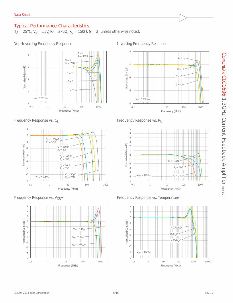
Typical Performance CharacteristicsTA = 25°C, Vs = ±5V, Rf = 270Ω, RL = 150Ω, G = 2; unless otherwise noted.
Frequency Response vs. VOUT Frequency Response vs. Temperature
Frequency Response vs. CL Frequency Response vs. RL
Non-Inverting Frequency Response Inverting Frequency Response
-9
-6
-3
0
3
0.1 1 10 100 1000
Nor
mal
ized
Gai
n (d
B)
Frequency (MHz)
G = 1Rf = 390Ω
G = 2
G = 5
G = 10
VOUT = 0.5Vpp
G = 1Rf = 499Ω
-9
-6
-3
0
3
0.1 1 10 100 1000
Nor
mal
ized
Gai
n (d
B)
Frequency (MHz)
G = -1
G = -2
G = -5
G = -10
VOUT = 0.5Vpp
-7
-6
-5
-4
-3
-2
-1
0
1
0.1 1 10 100 1000
Nor
mal
ized
Gai
n (d
B)
Frequency (MHz)
CL = 1000pFRs = 3.3Ω
CL = 500pFRs = 5Ω
CL = 100pFRs = 10Ω
CL = 50pFRs = 15Ω
CL = 20pFRs = 20ΩVOUT = 0.5Vpp
-6
-5
-4
-3
-2
-1
0
1
2
3
4
5
6
0.1 1 10 100 1000
Nor
mal
ized
Gai
n (d
B)
Frequency (MHz)
VOUT = 0.5Vpp
RL = 100Ω
RL = 50Ω
RL = 25Ω
-7
-6
-5
-4
-3
-2
-1
0
1
2
3
0.1 1 10 100 1000
Nor
mal
ized
Gai
n (d
B)
Frequency (MHz)
VOUT = 1Vpp
VOUT = 2Vpp
VOUT = 4Vpp
-7
-6
-5
-4
-3
-2
-1
0
1
2
0.1 1 10 100 1000 10000
Nor
mal
ized
Gai
n (d
B)
Frequency (MHz)
+ 85degC
- 40degC
+ 25degC
VOUT = 0.2Vpp
Data SheetC
om
linear CLC1606 1.3G
Hz C
urrent Feedback Amplifier R
ev 1D
©2007-2013 Exar Corporation 7/18 Rev 1D
Typical Performance CharacteristicsTA = 25°C, Vs = ±5V, Rf = 270Ω, RL = 150Ω, G = 2; unless otherwise noted.
Frequency Response vs. VOUT at VS = 5V Frequency Response vs. Temperature at VS = 5V
Frequency Response vs. CL at VS = 5V Frequency Response vs. RL at VS = 5V
Non-Inverting Frequency Response at VS = 5V Inverting Frequency Response at VS = 5V
-9
-8
-7
-6
-5
-4
-3
-2
-1
0
1
2
0.1 1 10 100 1000
Nor
mal
ized
Gai
n (d
B)
Frequency (MHz)
G = 1Rf = 390Ω
G = 2
G = 5
G = 10
VOUT = 0.5Vpp
-9
-6
-3
0
3
0.1 1 10 100 1000
Nor
mal
ized
Gai
n (d
B)
Frequency (MHz)
G = -1
G = -2
G = -5
G = -10
VOUT = 0.5Vpp
-7
-6
-5
-4
-3
-2
-1
0
1
0.1 1 10 100 1000
Nor
mal
ized
Gai
n (d
B)
Frequency (MHz)
CL = 1000pFRs = 3.3Ω
CL = 500pFRs = 5Ω
CL = 100pFRs = 10Ω
CL = 50pFRs = 15Ω
CL = 20pFRs = 20ΩVOUT = 0.5Vpp
-6
-5
-4
-3
-2
-1
0
1
2
3
4
0.1 1 10 100 1000
Nor
mal
ized
Gai
n (d
B)
Frequency (MHz)
VOUT = 0.5Vpp
RL = 100Ω
RL = 50Ω
RL = 25Ω
-7
-6
-5
-4
-3
-2
-1
0
1
2
0.1 1 10 100 1000
Nor
mal
ized
Gai
n (d
B)
Frequency (MHz)
VOUT = 1Vpp
VOUT = 2Vpp
VOUT = 3Vpp
-7
-6
-5
-4
-3
-2
-1
0
1
2
0.1 1 10 100 1000 10000
Nor
mal
ized
Gai
n (d
B)
Frequency (MHz)
+ 85degC
- 40degC
+ 25degC
VOUT = 0.2Vpp
Data SheetC
om
linear CLC1606 1.3G
Hz C
urrent Feedback Amplifier R
ev 1D
©2007-2013 Exar Corporation 8/18 Rev 1D
Typical Performance Characteristics - ContinuedTA = 25°C, Vs = ±5V, Rf = 270Ω, RL = 150Ω, G = 2; unless otherwise noted.
Closed Loop Output Impedance vs. Frequency Input Voltage Noise
-3dB Bandwidth vs. VOUT at G=10 -3dB Bandwidth vs. VOUT at G=10, VS = 5V
Gain Flatness Gain Flatness at VS = 5V
-0.5
-0.3
-0.1
0.1
0.3
0.5
0.7
0.9
1.1
1.3
1.5
1.7
0.1 1 10 100 1000
Nor
mal
ized
Gai
n (d
B)
Frequency (MHz)
VOUT = 2VppRL = 150ΩRf = 270Ω
-0.5
-0.4
-0.3
-0.2
-0.1
0
0.1
0.2
0.3
0.4
0.5
0.6
0.7
0.8
0.1 1 10 100 1000
Nor
mal
ized
Gai
n (d
B)
Frequency (MHz)
VOUT = 2VppRL = 150ΩRf = 270Ω
300
350
400
450
500
550
600
0.0 0.5 1.0 1.5 2.0 2.5 3.0 3.5 4.0
-3dB
Ban
dwid
th (
MH
z)
VOUT (VPP)
G = 10
250
300
350
400
450
0.0 0.5 1.0 1.5 2.0 2.5 3.0
-3dB
Ban
dwid
th (
MH
z)
VOUT (VPP)
Out
put
Resi
stan
ce (
Ω)
Frequency (Hz)10K 100K 1M 10M 100M
0
0.2
0.4
0.6
0.8
1.0
1.2
1.4
1.6
1.8
2.0VS = ±5.0V
Inpu
t Vo
ltage
Noi
se (
nV/√
Hz)
Frequency (MHz)0.0001 0.001 0.01 0.1 1 100
5
10
15
20
Data SheetC
om
linear CLC1606 1.3G
Hz C
urrent Feedback Amplifier R
ev 1D
©2007-2013 Exar Corporation 9/18 Rev 1D
Typical Performance Characteristics - ContinuedTA = 25°C, Vs = ±5V, Rf = 270Ω, RL = 150Ω, G = 2; unless otherwise noted.
CMRR vs. Frequency PSRR vs. Frequency
2nd Harmonic Distortion vs. VOUT 3rd Harmonic Distortion vs. VOUT
2nd Harmonic Distortion vs. RL 3rd Harmonic Distortion vs. RL
-100
-95
-90
-85
-80
-75
-70
-65
-60
-55
0 5 10 15 20
Dis
tort
ion
(dBc
)
Frequency (MHz)
RL = 150Ω
VOUT = 2Vpp
RL = 499Ω
-100
-95
-90
-85
-80
-75
-70
-65
-60
-55
0 5 10 15 20
Dis
tort
ion
(dBc
)
Frequency (MHz)
RL = 150Ω
VOUT = 2Vpp
RL = 499Ω
-90
-85
-80
-75
-70
-65
-60
0.5 0.75 1 1.25 1.5 1.75 2 2.25 2.5
Dis
tort
ion
(dBc
)
Output Amplitude (Vpp)
10MHz
5MHz
1MHz
RL = 150Ω-95
-90
-85
-80
-75
-70
-65
-60
0.5 0.75 1 1.25 1.5 1.75 2 2.25 2.5
Dis
tort
ion
(dBc
)
Output Amplitude (Vpp)
10MHz
5MHz
1MHz
RL = 150Ω
CMRR (
dB)
Frequency (Hz)10k 100k 1M 10M 100M
-60
-50
-40
-30
-20
-10
0VS = ±5.0V
PSRR (
dB)
Frequency (Hz)10K 100K 1M 10M 100M
-60
-50
-40
-30
-20
-10
0
Data SheetC
om
linear CLC1606 1.3G
Hz C
urrent Feedback Amplifier R
ev 1D
©2007-2013 Exar Corporation 10/18 Rev 1D
Typical Performance Characteristics - ContinuedTA = 25°C, Vs = ±5V, Rf = 270Ω, RL = 150Ω, G = 2; unless otherwise noted.
Differential Gain & Phase AC Coupled Output Differential Gain & Phase DC Coupled Output
Large Signal Pulse Response Large Signal Pulse Response at VS = 5V
Small Signal Pulse Response Small Signal Pulse Response at VS = 5V
-0.125
-0.1
-0.075
-0.05
-0.025
0
0.025
0.05
0.075
0.1
0.125
0 20 40 60 80 100 120 140 160 180 200
Volta
ge (V
)
Time (ns)
2.375
2.4
2.425
2.45
2.475
2.5
2.525
2.55
2.575
2.6
2.625
0 20 40 60 80 100 120 140 160 180 200
Volta
ge (V
)
Time (ns)
-3
-2
-1
0
1
2
3
0 20 40 60 80 100 120 140 160 180 200
Volta
ge (V
)
Time (ns)
1
1.5
2
2.5
3
3.5
4
0 20 40 60 80 100 120 140 160 180 200
Volta
ge (V
)
Time (ns)
-0.015
-0.01
-0.005
0
0.005
0.01
0.015
0.02
-0.7 -0.5 -0.3 -0.1 0.1 0.3 0.5 0.7
Diff
Gai
n (%
) /
Diff
Pha
se (
°)
Input Voltage (V)
DG
RL = 150ΩAC coupled
DP
-0.02
-0.01
0
0.01
0.02
0.03
0.04
0.05
0.06
-0.7 -0.5 -0.3 -0.1 0.1 0.3 0.5 0.7
Diff
Gai
n (%
) /
Diff
Pha
se (
°)
Input Voltage (V)
DG
RL = 150ΩDC coupled
DP

Data SheetC
om
linear CLC1606 1.3G
Hz C
urrent Feedback Amplifier R
ev 1D
©2007-2013 Exar Corporation 11/18 Rev 1D
Typical Performance Characteristics - ContinuedTA = 25°C, Vs = ±5V, Rf = 270Ω, RL = 150Ω, G = 2; unless otherwise noted.
Differential Gain & Phase AC Coupled Output at VS = ±2.5V Differential Gain & Phase DC Coupled at VS = ±2.5V
-0.03
-0.025
-0.02
-0.015
-0.01
-0.005
0
0.005
0.01
-0.35 -0.25 -0.15 -0.05 0.05 0.15 0.25 0.35
Diff
Gai
n (%
) /
Diff
Pha
se (
° )
Input Voltage (V)
RL = 150ΩDC coupled
DP
DG
RL = 150ΩAC coupled
-0.04
-0.03
-0.02
-0.01
0
0.01
0.02
0.03
0.04
0.05
-0.35 -0.25 -0.15 -0.05 0.05 0.15 0.25 0.35
Diff
Gai
n (%
) /
Diff
Pha
se (
°)
Input Voltage (V)
RL = 150ΩDC coupled
DP
DG
RL = 150ΩDC coupled
Data SheetC
om
linear CLC1606 1.3G
Hz C
urrent Feedback Amplifier R
ev 1D
©2007-2013 Exar Corporation 12/18 Rev 1D
General Information - Current Feedback Technology
Advantages of CFB Technology
The CLC1606 Family of amplifiers utilize current feedback (CFB) technology to achieve superior performance. The primary advantage of CFB technology is higher slew rate performance when compared to voltage feedback (VFB) architecture. High slew rate contributes directly to better large signal pulse response, full power bandwidth, and distortion.
CFB also alleviates the traditional trade-off between closed loop gain and usable bandwidth that is seen with a VFB amplifier. With CFB, the bandwidth is primarily determined by the value of the feedback resistor, Rf. By using optimum feedback resistor values, the bandwidth of a CFB amplifier remains nearly constant with different gain configurations.
When designing with CFB amplifiers always abide by these basic rules:
• Use the recommended feedback resistor value
• Do not use reactive (capacitors, diodes, inductors, etc.) elements in the direct feedback path
• Avoid stray or parasitic capacitance across feedback resistors
• Follow general high-speed amplifier layout guidelines
• Ensure proper precautions have been made for driving capacitive loads
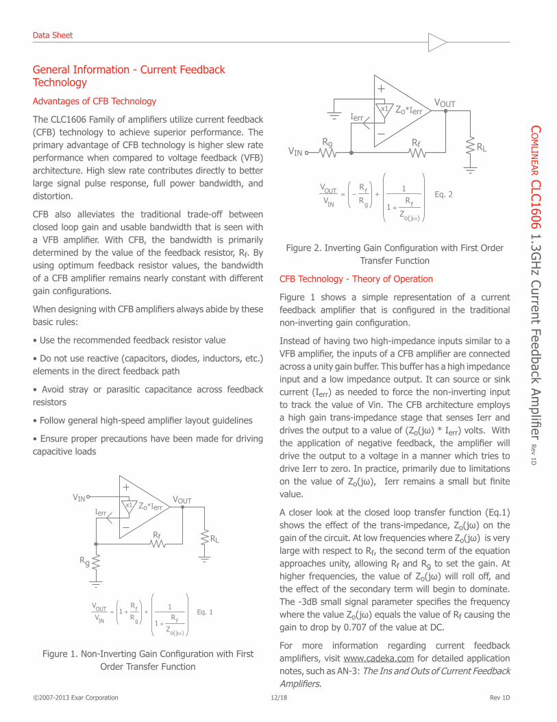
Figure 1. Non-Inverting Gain Configuration with First Order Transfer Function
VOUT
VIN
= −RfRg
+1
Eq. 2
1 +Rf
Zo(jω)
VIN
VOUTZo*IerrIerr
RLRf
x1
Rg
Figure 2. Inverting Gain Configuration with First Order Transfer Function
CFB Technology - Theory of Operation
Figure 1 shows a simple representation of a current feedback amplifier that is configured in the traditional non-inverting gain configuration.
Instead of having two high-impedance inputs similar to a VFB amplifier, the inputs of a CFB amplifier are connected across a unity gain buffer. This buffer has a high impedance input and a low impedance output. It can source or sink current (Ierr) as needed to force the non-inverting input to track the value of Vin. The CFB architecture employs a high gain trans-impedance stage that senses Ierr and drives the output to a value of (Zo(jω) * Ierr) volts. With the application of negative feedback, the amplifier will drive the output to a voltage in a manner which tries to drive Ierr to zero. In practice, primarily due to limitations on the value of Zo(jω), Ierr remains a small but finite value.
A closer look at the closed loop transfer function (Eq.1) shows the effect of the trans-impedance, Zo(jω) on the gain of the circuit. At low frequencies where Zo(jω) is very large with respect to Rf, the second term of the equation approaches unity, allowing Rf and Rg to set the gain. At higher frequencies, the value of Zo(jω) will roll off, and the effect of the secondary term will begin to dominate. The -3dB small signal parameter specifies the frequency where the value Zo(jω) equals the value of Rf causing the gain to drop by 0.707 of the value at DC.
For more information regarding current feedback amplifiers, visit www.cadeka.com for detailed application notes, such as AN-3: The Ins and Outs of Current Feedback Amplifiers.
VOUT
VIN
= 1 +RfRg
+1
Eq. 1
1 +Rf
Zo(jω)
VIN VOUTZo*IerrIerr
Rg
RLRf
x1

Data SheetC
om
linear CLC1606 1.3G
Hz C
urrent Feedback Amplifier R
ev 1D
©2007-2013 Exar Corporation 13/18 Rev 1D
Application Information
Basic Operation
Figures 3, 4, and 5 illustrate typical circuit configurations for non-inverting, inverting, and unity gain topologies for dual supply applications. They show the recommended bypass capacitor values and overall closed loop gain equations.
Figure 3. Typical Non-Inverting Gain Circuit
Figure 4. Typical Inverting Gain Circuit
Figure 5. Typical Unity Gain (G=1) Circuit
CFB amplifiers can be used in unity gain configurations. Do not use the traditional voltage follower circuit, where the output is tied directly to the inverting input. With a CFB amplifier, a feedback resistor of appropriate value must be used to prevent unstable behavior. Refer to figure 5 and Table 1. Although this seems cumbersome, it does allow a degree of freedom to adjust the passband characteristics.
Feedback Resistor Selection
One of the key design considerations when using a CFB amplifier is the selection of the feedback resistor, Rf. Rf is used in conjunction with Rg to set the gain in the traditional non-inverting and inverting circuit configurations. Refer to figures 3 and 4. As discussed in the Current Feedback Technology section, the value of the feedback resistor has a pronounced effect on the frequency response of the circuit.
Table 1, provides recommended Rf and associated Rg values for various gain settings. These values produce the optimum frequency response, maximum bandwidth with minimum peaking. Adjust these values to optimize performance for a specific application. The typical performance characteristics section includes plots that illustrate how the bandwidth is directly affected by the value of Rf at various gain settings.
Gain (V/V
Rf (Ω) Rg (Ω) ±0.1dB BW
(MHz)-3dB BW (MHz)
1 390 - 136 1300
2 270 270 150 1200
5 270 67.5 115 750
Table 1: Recommended Rf vs. Gain
In general, lowering the value of Rf from the recommended value will extend the bandwidth at the expense of additional high frequency gain peaking. This will cause increased overshoot and ringing in the pulse response characteristics. Reducing Rf too much will eventually cause oscillatory behavior.
Increasing the value of Rf will lower the bandwidth. Lowering the bandwidth creates a flatter frequency response and improves 0.1dB bandwidth performance. This is important in applications such as video. Further increase in Rf will cause premature gain rolloff and adversely affect gain flatness.
+
-
Rf
0.1μF
6.8μF
Output
G = - (Rf/Rg)
For optimum input offsetvoltage set R1 = Rf || Rg
Input
+Vs
-Vs
0.1μF
6.8μF
RL
Rg
R1
+
-
Rf
0.1μF
6.8μF
Output
G = 1
Rf is required for CFB amplifiers
Input
+Vs
-Vs
0.1μF
6.8μF
RL
+
-
Rf
0.1μF
6.8μF
Output
G = 1 + (Rf/Rg)
Input
+Vs
-Vs
Rg
0.1μF
6.8μF
RL
Data SheetC
om
linear CLC1606 1.3G
Hz C
urrent Feedback Amplifier R
ev 1D
©2007-2013 Exar Corporation 14/18 Rev 1D
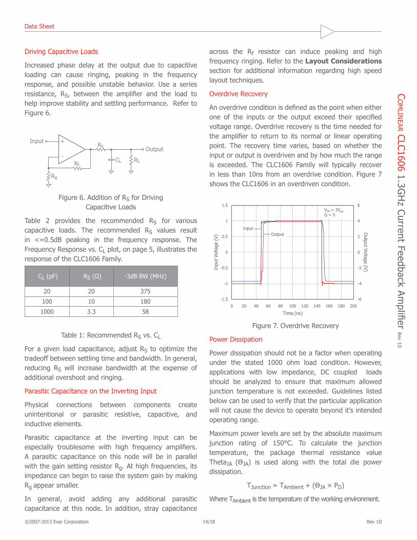
Driving Capacitive Loads
Increased phase delay at the output due to capacitive loading can cause ringing, peaking in the frequency response, and possible unstable behavior. Use a series resistance, RS, between the amplifier and the load to help improve stability and settling performance. Refer to Figure 6.
Figure 6. Addition of RS for Driving Capacitive Loads
Table 2 provides the recommended RS for various capacitive loads. The recommended RS values result in <=0.5dB peaking in the frequency response. The Frequency Response vs. CL plot, on page 5, illustrates the response of the CLC1606 Family.
CL (pF) RS (Ω) -3dB BW (MHz)
20 20 375
100 10 180
1000 3.3 58
Table 1: Recommended RS vs. CL
For a given load capacitance, adjust RS to optimize the tradeoff between settling time and bandwidth. In general, reducing RS will increase bandwidth at the expense of additional overshoot and ringing.
Parasitic Capacitance on the Inverting Input
Physical connections between components create unintentional or parasitic resistive, capacitive, and inductive elements.
Parasitic capacitance at the inverting input can be especially troublesome with high frequency amplifiers. A parasitic capacitance on this node will be in parallel with the gain setting resistor Rg. At high frequencies, its impedance can begin to raise the system gain by making Rg appear smaller.
In general, avoid adding any additional parasitic capacitance at this node. In addition, stray capacitance
across the Rf resistor can induce peaking and high frequency ringing. Refer to the Layout Considerations section for additional information regarding high speed layout techniques.
Overdrive Recovery
An overdrive condition is defined as the point when either one of the inputs or the output exceed their specified voltage range. Overdrive recovery is the time needed for the amplifier to return to its normal or linear operating point. The recovery time varies, based on whether the input or output is overdriven and by how much the range is exceeded. The CLC1606 Family will typically recover in less than 10ns from an overdrive condition. Figure 7 shows the CLC1606 in an overdriven condition.
Figure 7. Overdrive Recovery
Power Dissipation
Power dissipation should not be a factor when operating under the stated 1000 ohm load condition. However, applications with low impedance, DC coupled loads should be analyzed to ensure that maximum allowed junction temperature is not exceeded. Guidelines listed below can be used to verify that the particular application will not cause the device to operate beyond it’s intended operating range.
Maximum power levels are set by the absolute maximum junction rating of 150°C. To calculate the junction temperature, the package thermal resistance value ThetaJA (ӨJA) is used along with the total die power dissipation.
TJunction = TAmbient + (ӨJA × PD)
Where TAmbient is the temperature of the working environment.
+
-Rf
InputOutput
Rg
Rs
CL RL
-6
-4
-2
0
2
4
6
-1.5
-1
-0.5
0
0.5
1
1.5
0 20 40 60 80 100 120 140 160 180 200
Output Voltage (V)In
put V
olta
ge (
V)
Time (ns)
OutputInput
VIN = 2VppG = 5
Data SheetC
om
linear CLC1606 1.3G
Hz C
urrent Feedback Amplifier R
ev 1D
©2007-2013 Exar Corporation 15/18 Rev 1D
In order to determine PD, the power dissipated in the load needs to be subtracted from the total power delivered by the supplies.
PD = Psupply - Pload
Supply power is calculated by the standard power equation.
Psupply = Vsupply × IRMS supply
Vsupply = VS+ - VS-
Power delivered to a purely resistive load is:
Pload = ((VLOAD)RMS2)/Rloadeff
The effective load resistor (Rloadeff) will need to include the effect of the feedback network. For instance,
Rloadeff in figure 3 would be calculated as:
RL || (Rf + Rg)
These measurements are basic and are relatively easy to perform with standard lab equipment. For design purposes however, prior knowledge of actual signal levels and load impedance is needed to determine the dissipated power. Here, PD can be found from
PD = PQuiescent + PDynamic - PLoad
Quiescent power can be derived from the specified IS values along with known supply voltage, VSupply. Load power can be calculated as above with the desired signal amplitudes using:
(VLOAD)RMS = VPEAK / √2
( ILOAD)RMS = ( VLOAD)RMS / Rloadeff
The dynamic power is focused primarily within the output stage driving the load. This value can be calculated as:
PDYNAMIC = (VS+ - VLOAD)RMS × ( ILOAD)RMS
Assuming the load is referenced in the middle of the power rails or Vsupply/2.
Figure 8 shows the maximum safe power dissipation in the package vs. the ambient temperature for the 8 and 14 lead SOIC packages.
0
0.5
1
1.5
2
-40 -20 0 20 40 60 80
Max
imum
Pow
er D
issi
patio
n (W
)
Ambient Temperature (°C)
SOT23-5
SOIC-8
Figure 8. Maximum Power Derating
Better thermal ratings can be achieved by maximizing PC board metallization at the package pins. However, be careful of stray capacitance on the input pins.
In addition, increased airflow across the package can also help to reduce the effective ӨJA of the package.
In the event the outputs are momentarily shorted to a low impedance path, internal circuitry and output metallization are set to limit and handle up to 65mA of output current. However, extended duration under these conditions may not guarantee that the maximum junction temperature (+150°C) is not exceeded.
Layout Considerations
General layout and supply bypassing play major roles in high frequency performance. Exar has evaluation boards to use as a guide for high frequency layout and as aid in device testing and characterization. Follow the steps below as a basis for high frequency layout:
Include 6.8µF and 0.1µF ceramic capacitors for power supply decoupling
Place the 6.8µF capacitor within 0.75 inches of the power pin
Place the 0.1µF capacitor within 0.1 inches of the power pin
Remove the ground plane under and around the part, especially near the input and output pins to reduce parasitic capacitance
Minimize all trace lengths to reduce series inductances
Refer to the evaluation board layouts below for more information.
Data SheetC
om
linear CLC1606 1.3G
Hz C
urrent Feedback Amplifier R
ev 1D
©2007-2013 Exar Corporation 16/18 Rev 1D
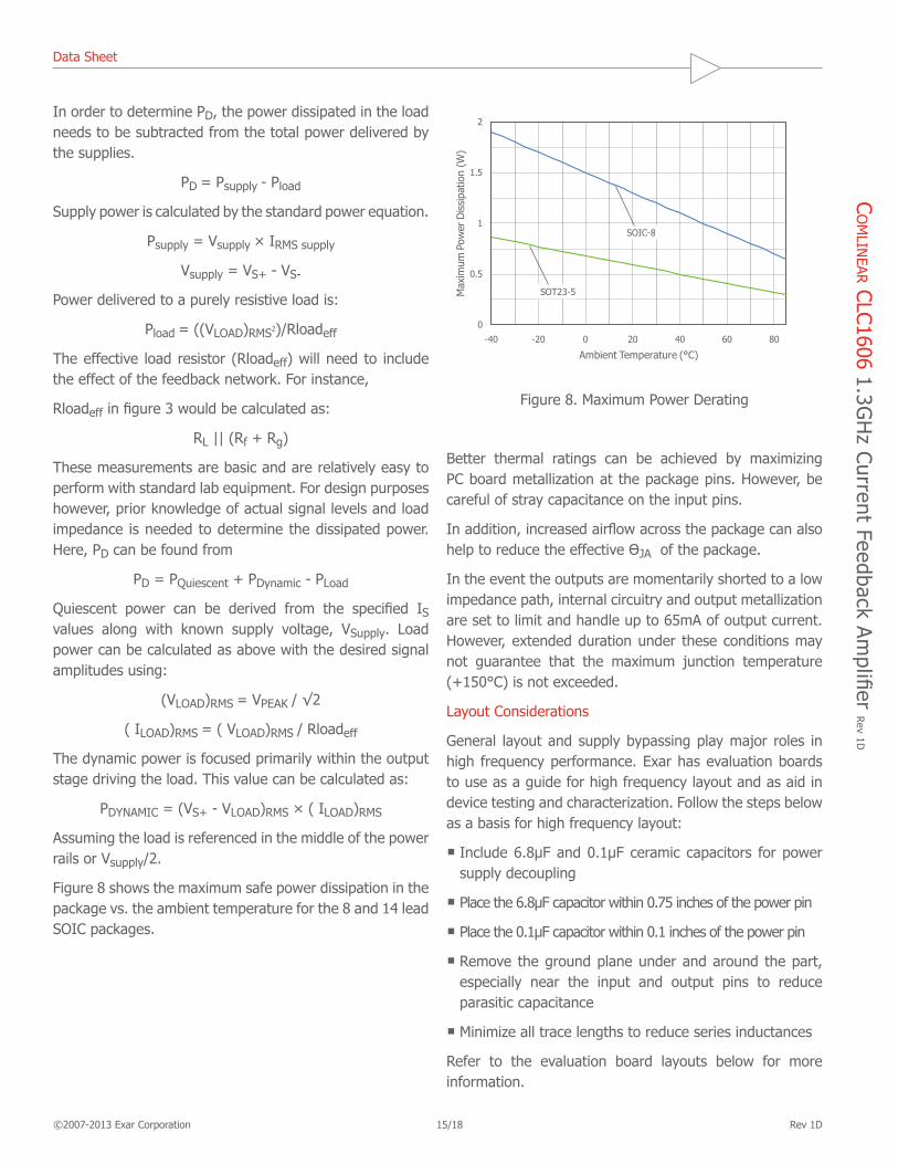
Evaluation Board Information
The following evaluation boards are available to aid in the testing and layout of these devices:
Evaluation Board # ProductsCEB002 CLC1606IST5XCEB003 CLC1606ISO8X
Evaluation Board Schematics
Evaluation board schematics and layouts are shown in Figures 9-14. These evaluation boards are built for dual- supply operation. Follow these steps to use the board in a single-supply application:
1. Short -Vs to ground.
2. Use C3 and C4, if the -VS pin of the amplifier is not directly connected to the ground plane.
Figure 9. CEB002 Schematic
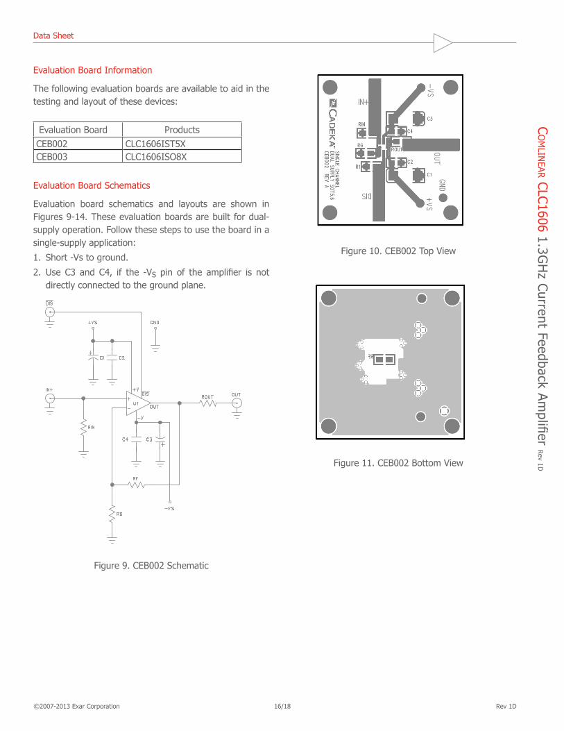
Figure 10. CEB002 Top View
Figure 11. CEB002 Bottom View
Data SheetC
om
linear CLC1606 1.3G
Hz C
urrent Feedback Amplifier R
ev 1D
©2007-2013 Exar Corporation 17/18 Rev 1D
Figure 12. CEB003 Schematic
Figure 13. CEB003 Top View
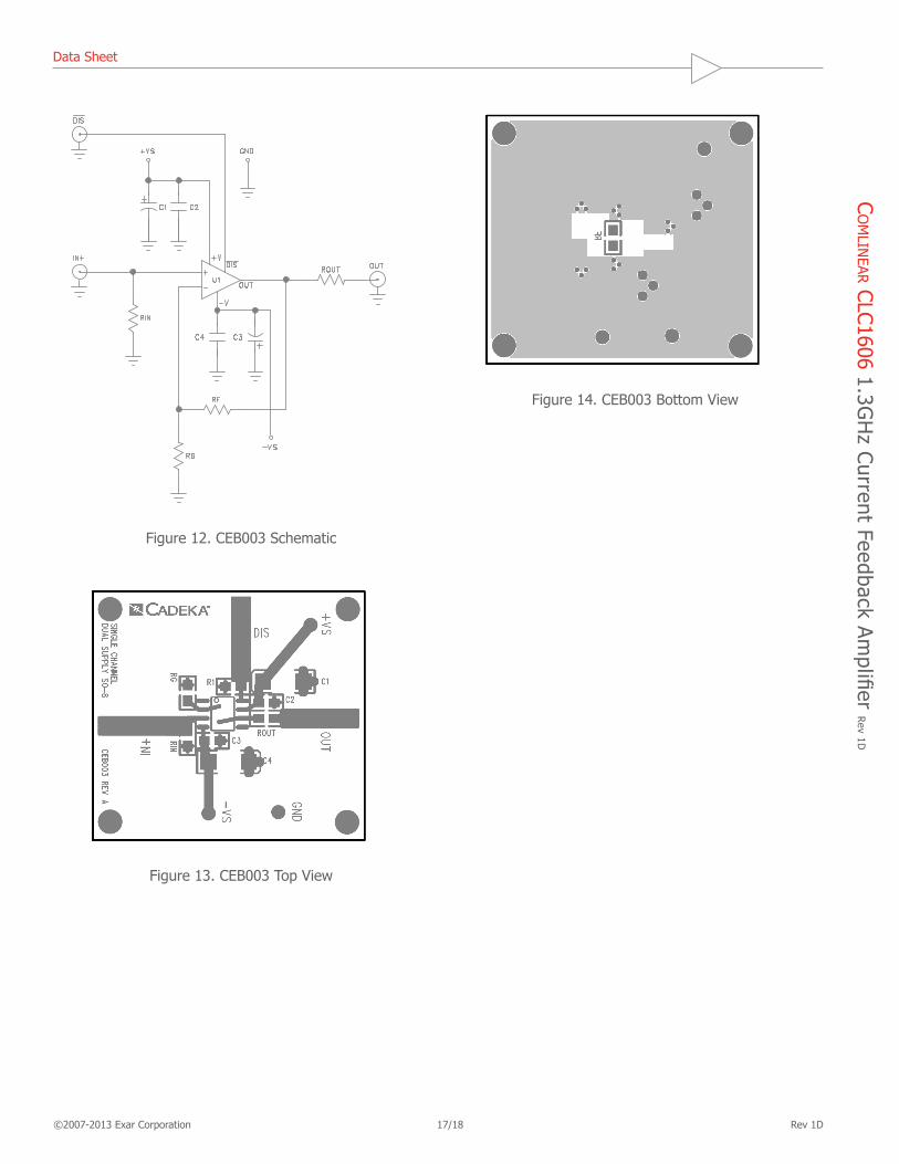
Figure 14. CEB003 Bottom View

Data SheetC
om
linear CLC1606 1.3G
Hz C
urrent Feedback Amplifier R
ev 1D
For Further Assistance:Exar Corporation Headquarters and Sales Offices 48720 Kato Road Tel.: +1 (510) 668-7000Fremont, CA 94538 - USA Fax: +1 (510) 668-7001 www.exar.com
NOTICE
EXAR Corporation reserves the right to make changes to the products contained in this publication in order to improve design, performance or reliability. EXAR Corporation assumes no responsibility for the use of any circuits described herein, conveys no license under any patent or other right, and makes no representation that the circuits are free of patent infringement. Charts and schedules contained here in are only for illustration purposes and may vary depending upon a user’s specific application. While the information in this publication has been carefully checked; no responsibility, however, is assumed for inaccuracies.
EXAR Corporation does not recommend the use of any of its products in life support applications where the failure or malfunction of the product can reasonably be expected to cause failure of the life support system or to significantly affect its safety or effectiveness. Products are not authorized for use in such applications unless EXAR Corporation receives, in writing, assurances to its satisfaction that: (a) the risk of injury or damage has been minimized; (b) the user assumes all such risks; (c) potential liability of EXAR Corporation is adequately protected under the circumstances.
Reproduction, in part or whole, without the prior written consent of EXAR Corporation is prohibited.
©2007-2013 Exar Corporation 18/18 Rev 1D
Mechanical Dimensions
SOT23-5 Package
SOIC-8 Package