N-channel 400 V, 2.7 typ., 2 A SuperMESH3 Zener-protected ...
16
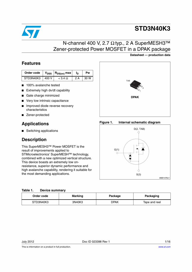
This is information on a product in full production. July 2012 Doc ID 023398 Rev 1 1/16 16 STD3N40K3 N-channel 400 V, 2.7 Ω typ., 2 A SuperMESH3™ Zener-protected Power MOSFET in a DPAK package Datasheet — production data Features ■ 100% avalanche tested ■ Extremely high dv/dt capability ■ Gate charge minimized ■ Very low intrinsic capacitance ■ Improved diode reverse recovery characteristics ■ Zener-protected Applications ■ Switching applications Description This SuperMESH3™ Power MOSFET is the result of improvements applied to STMicroelectronics’ SuperMESH™ technology, combined with a new optimized vertical structure. This device boasts an extremely low on- resistance, superior dynamic performance and high avalanche capability, rendering it suitable for the most demanding applications. Figure 1. Internal schematic diagram Order code V DSS R DS(on) max I D Pw STD3N40K3 400 V < 3.4 Ω 2 A 30 W DPAK 1 3 TAB AM01476v1 Table 1. Device summary Order code Marking Package Packaging STD3N40K3 3N40K3 DPAK Tape and reel www.st.com
Transcript of N-channel 400 V, 2.7 typ., 2 A SuperMESH3 Zener-protected ...
This is information on a product in full production.
July 2012 Doc ID 023398 Rev 1 1/16
16
STD3N40K3
N-channel 400 V, 2.7 Ω typ., 2 A SuperMESH3™ Zener-protected Power MOSFET in a DPAK package
Datasheet — production data
Features
■ 100% avalanche tested
■ Extremely high dv/dt capability
■ Gate charge minimized
■ Very low intrinsic capacitance
■ Improved diode reverse recovery characteristics
■ Zener-protected
Applications■ Switching applications
DescriptionThis SuperMESH3™ Power MOSFET is the result of improvements applied to STMicroelectronics’ SuperMESH™ technology, combined with a new optimized vertical structure. This device boasts an extremely low on- resistance, superior dynamic performance and high avalanche capability, rendering it suitable for the most demanding applications.
Figure 1. Internal schematic diagram
Order code VDSS RDS(on) max ID Pw
STD3N40K3 400 V < 3.4 Ω 2 A 30 W
DPAK
1
3
TAB
AM01476v1
Table 1. Device summary
Order code Marking Package Packaging
STD3N40K3 3N40K3 DPAK Tape and reel
www.st.com
Contents STD3N40K3
2/16 Doc ID 023398 Rev 1
Contents
1 Electrical ratings . . . . . . . . . . . . . . . . . . . . . . . . . . . . . . . . . . . . . . . . . . . . 3
2 Electrical characteristics . . . . . . . . . . . . . . . . . . . . . . . . . . . . . . . . . . . . . 4
2.1 Electrical characteristics (curves) . . . . . . . . . . . . . . . . . . . . . . . . . . . . . 6
3 Test circuits . . . . . . . . . . . . . . . . . . . . . . . . . . . . . . . . . . . . . . . . . . . . . . 9
4 Package mechanical data . . . . . . . . . . . . . . . . . . . . . . . . . . . . . . . . . . . . 10
5 Packaging mechanical data . . . . . . . . . . . . . . . . . . . . . . . . . . . . . . . . . . 13
6 Revision history . . . . . . . . . . . . . . . . . . . . . . . . . . . . . . . . . . . . . . . . . . . 15
STD3N40K3 Electrical ratings
Doc ID 023398 Rev 1 3/16
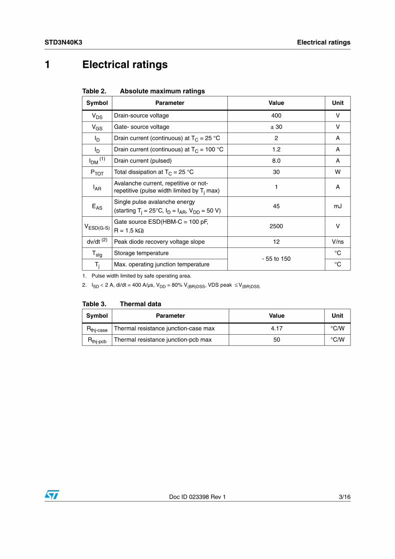
1 Electrical ratings
Table 2. Absolute maximum ratings
Symbol Parameter Value Unit
VDS Drain-source voltage 400 V
VGS Gate- source voltage ± 30 V
ID Drain current (continuous) at TC = 25 °C 2 A
ID Drain current (continuous) at TC = 100 °C 1.2 A
IDM (1)
1. Pulse width limited by safe operating area.
Drain current (pulsed) 8.0 A
PTOT Total dissipation at TC = 25 °C 30 W
IARAvalanche current, repetitive or not-repetitive (pulse width limited by Tj max)
1 A
EASSingle pulse avalanche energy
(starting Tj = 25°C, ID = IAR, VDD = 50 V)45 mJ
VESD(G-S)Gate source ESD(HBM-C = 100 pF,
R = 1.5 kΩ)2500 V
dv/dt (2)
2. ISD < 2 A, di/dt = 400 A/µs, VDD = 80% V(BR)DSS, VDS peak ≤ V(BR)DSS.
Peak diode recovery voltage slope 12 V/ns
Tstg Storage temperature- 55 to 150
°C
Tj Max. operating junction temperature °C
Table 3. Thermal data
Symbol Parameter Value Unit
Rthj-case Thermal resistance junction-case max 4.17 °C/W
Rthj-pcb Thermal resistance junction-pcb max 50 °C/W
Electrical characteristics STD3N40K3
4/16 Doc ID 023398 Rev 1
2 Electrical characteristics
(TC = 25 °C unless otherwise specified)
Table 4. On /off states
Symbol Parameter Test conditions Min. Typ. Max. Unit
V(BR)DSSDrain-source breakdown voltage
ID = 1 mA, VGS = 0 400 V
IDSSZero gate voltage drain current (VGS = 0)
VDS = 400 VVDS = 400 V, TC=125 °C
150
µAµA
IGSSGate-body leakagecurrent (VDS = 0)
VGS = ± 20 V, VDS=0 ±10 µA
VGS(th) Gate threshold voltage VGS = VDS, ID = 50 µA 3 3.75 4.5 V
RDS(on)Static drain-source on- resistance
VGS = 10 V, ID = 0.9 A 2.7 3.4 Ω
Table 5. Dynamic
Symbol Parameter Test conditions Min. Typ. Max. Unit
Ciss
Coss
Crss
Input capacitanceOutput capacitanceReverse transfer capacitance
VDS = 50 V, f = 1 MHz, VGS = 0
-
165173
-pFpFpF
Coss(er)(1)
1. Is defined as a constant equivalent capacitance giving the same charging time as Coss when VDS increases from 0 to 80% VDSS
Equivalent output capacitance energy related
VDS=0 to 320 V, VGS=0
- 9 - pF
Coss(tr)(2)
2. Is defined as a constant equivalent capacitance giving the same storage energy as Coss when VDS increases from 0 to 80% VDSS
Equivalent output capacitance time related
- 14 - pF
RgInstrinsic gate resistance
f=1 MHz open drain - 10 - Ω
Qg
Qgs
Qgd
Total gate chargeGate-source charge
Gate-drain charge
VDD = 320 V, ID = 1.8 A,VGS = 10 V
(see Figure 16)
-112
7
-nCnC
nC
STD3N40K3 Electrical characteristics
Doc ID 023398 Rev 1 5/16
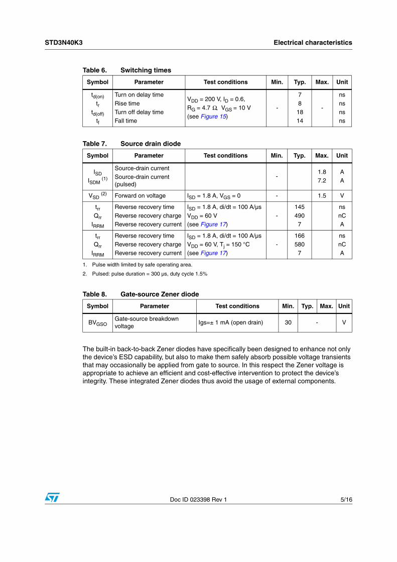
The built-in back-to-back Zener diodes have specifically been designed to enhance not only the device’s ESD capability, but also to make them safely absorb possible voltage transients that may occasionally be applied from gate to source. In this respect the Zener voltage is appropriate to achieve an efficient and cost-effective intervention to protect the device’s integrity. These integrated Zener diodes thus avoid the usage of external components.
Table 6. Switching times
Symbol Parameter Test conditions Min. Typ. Max. Unit
td(on)
trtd(off)
tf
Turn on delay time
Rise timeTurn off delay timeFall time
VDD = 200 V, ID = 0.6,
RG = 4.7 Ω, VGS = 10 V(see Figure 15)
-
7
81814
-
ns
nsnsns
Table 7. Source drain diode
Symbol Parameter Test conditions Min. Typ. Max. Unit
ISD
ISDM (1)
1. Pulse width limited by safe operating area.
Source-drain currentSource-drain current (pulsed)
-1.87.2
AA
VSD (2)
2. Pulsed: pulse duration = 300 µs, duty cycle 1.5%
Forward on voltage ISD = 1.8 A, VGS = 0 - 1.5 V
trrQrr
IRRM
Reverse recovery time
Reverse recovery chargeReverse recovery current
ISD = 1.8 A, di/dt = 100 A/µs
VDD = 60 V(see Figure 17)
-
145
4907
ns
nCA
trrQrr
IRRM
Reverse recovery timeReverse recovery chargeReverse recovery current
ISD = 1.8 A, di/dt = 100 A/µsVDD = 60 V, Tj = 150 °C(see Figure 17)
-166580
7
nsnCA
Table 8. Gate-source Zener diode
Symbol Parameter Test conditions Min. Typ. Max. Unit
BVGSOGate-source breakdown voltage
Igs=± 1 mA (open drain) 30 - V
Electrical characteristics STD3N40K3
6/16 Doc ID 023398 Rev 1
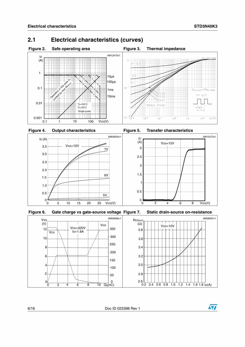
2.1 Electrical characteristics (curves) Figure 2. Safe operating area Figure 3. Thermal impedance
Figure 4. Output characteristics Figure 5. Transfer characteristics
Figure 6. Gate charge vs gate-source voltage Figure 7. Static drain-source on-resistance
ID
1
0.1
0.01
0.0010.1 1 100 VDS(V)10
(A)
Opera
tion
in th
is ar
ea is
Limite
d by
max
RDS(o
n)
10µs
100µs
1ms
10ms
Tj=150°CTc=25°C
Single pulse
AM12470v1
ID
1.5
1.0
0.5
00 10 VDS(V)20
(A)
5 15 25
2.0
2.5
5V
6V
7VVGS=10V
3.0
3.5
AM09050v1ID
1.5
1
0.5
00 4 VGS(V)8
(A)
2 6
2
2.5
3
VDS=15V
AM12473v1
VGS
6
4
2
00 2 Qg(nC)
(V)
8
8
4 6
10
VDD=320VID=1.8A
10
12
300
200
100
0
350VDS
VGS
150
250
50
AM08996v1RDS(on)
3.2
3.0
2.8
2.60.2 0.6 ID(A)
(Ω)
0.4 0.8
3.4
3.6
3.8VGS=10V
1.0 1.2 1.4 1.6 1.8
AM08997v1
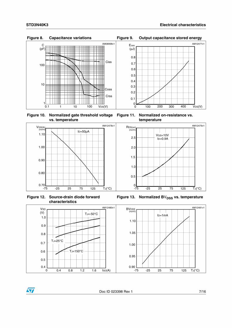
STD3N40K3 Electrical characteristics
Doc ID 023398 Rev 1 7/16
Figure 8. Capacitance variations Figure 9. Output capacitance stored energy
Figure 10. Normalized gate threshold voltage vs. temperature
Figure 11. Normalized on-resistance vs. temperature
Figure 12. Source-drain diode forward characteristics
Figure 13. Normalized BVDSS vs. temperature
C
100
10
10.1 10 VDS(V)
(pF)
1 100
Ciss
Coss
Crss
AM08998v1 Eoss
0.3
0.2
0.1
00 100 VDS(V)
(µJ)
400
0.4
200 300
0.5
0.6
0.7
0.8
AM12477v1
VGS(th)
1.00
0.90
0.80
0.70-75 TJ(°C)
(norm)
-25
1.10
7525 125
ID=50µA
AM12478v1 RDS(on)
2.0
1.5
1.0
0.5
-75 TJ(°C)
(norm)
-25 7525 125
2.5
0
VGS=10VID=0.9A
AM12479v1
VSD
0 0.8 ISD(A)
(V)
0.4 1.2 1.60.4
0.5
0.6
0.7
0.8
0.9
1.0TJ=-50°C
TJ=150°C
TJ=25°C
AM12480v1 BVDSS
-75 TJ(°C)
(norm)
-25 7525 1250.90
0.95
1.00
1.05
1.10
ID=1mA
AM12481v1
Electrical characteristics STD3N40K3
8/16 Doc ID 023398 Rev 1
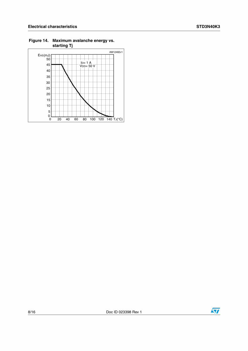
Figure 14. Maximum avalanche energy vs. starting Tj
EAS
0 40 TJ(°C)
(mJ)
20 10060 8005
10
15
20
120 140
25
30
35
40
45
50ID= 1 A
VDD= 50 V
AM12482v1
STD3N40K3 Test circuits
Doc ID 023398 Rev 1 9/16
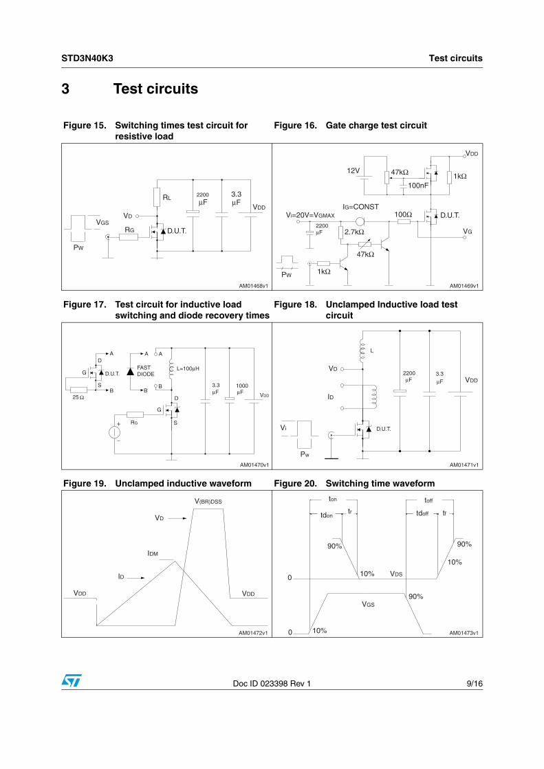
3 Test circuits
Figure 15. Switching times test circuit for resistive load
Figure 16. Gate charge test circuit
Figure 17. Test circuit for inductive load switching and diode recovery times
Figure 18. Unclamped Inductive load test circuit
Figure 19. Unclamped inductive waveform Figure 20. Switching time waveform
AM01468v1
VGS
PW
VD
RG
RL
D.U.T.
2200
μF3.3μF
VDD
AM01469v1
VDD
47kΩ 1kΩ
47kΩ
2.7kΩ
1kΩ
12V
Vi=20V=VGMAX
2200μF
PW
IG=CONST100Ω
100nF
D.U.T.
VG
AM01470v1
AD
D.U.T.
SB
G
25 Ω
A A
BB
RG
G
FASTDIODE
D
S
L=100μH
μF3.3 1000
μF VDD
AM01471v1
Vi
Pw
VD
ID
D.U.T.
L
2200μF
3.3μF VDD
AM01472v1
V(BR)DSS
VDDVDD
VD
IDM
ID
AM01473v1
VDS
ton
tdon tdoff
toff
tftr
90%
10%
10%
0
0
90%
90%
10%
VGS
Package mechanical data STD3N40K3
10/16 Doc ID 023398 Rev 1
4 Package mechanical data
In order to meet environmental requirements, ST offers these devices in different grades of ECOPACK® packages, depending on their level of environmental compliance. ECOPACK® specifications, grade definitions and product status are available at: www.st.com. ECOPACK® is an ST trademark.
STD3N40K3 Package mechanical data
Doc ID 023398 Rev 1 11/16
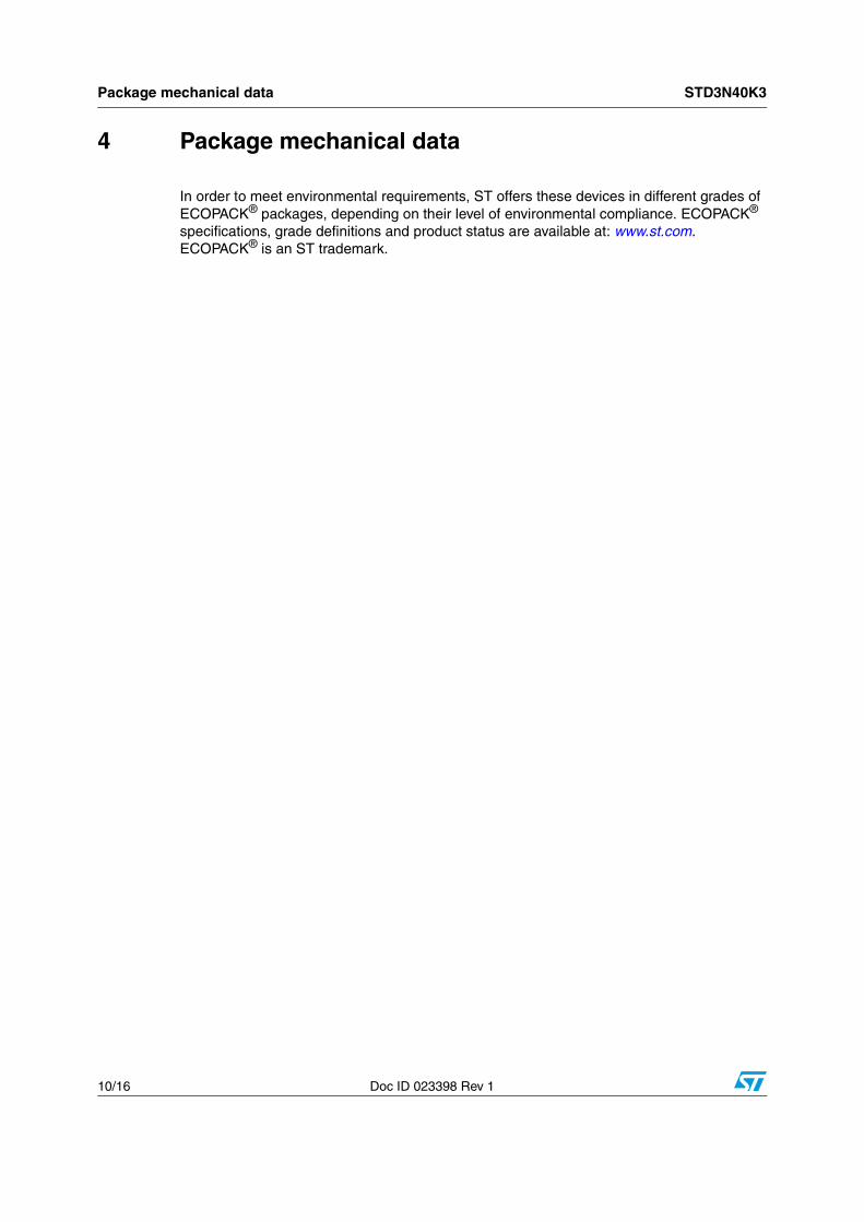
Table 9. DPAK (TO-252) mechanical data
Dim.mm
Min. Typ. Max.
A 2.20 2.40
A1 0.90 1.10
A2 0.03 0.23
b 0.64 0.90
b4 5.20 5.40
c 0.45 0.60
c2 0.48 0.60
D 6.00 6.20
D1 5.10
E 6.40 6.60
E1 4.70
e 2.28
e1 4.40 4.60
H 9.35 10.10
L 1 1.50
L1 2.80
L2 0.80
L4 0.60 1
R 0.20
V2 0° 8°
Package mechanical data STD3N40K3
12/16 Doc ID 023398 Rev 1
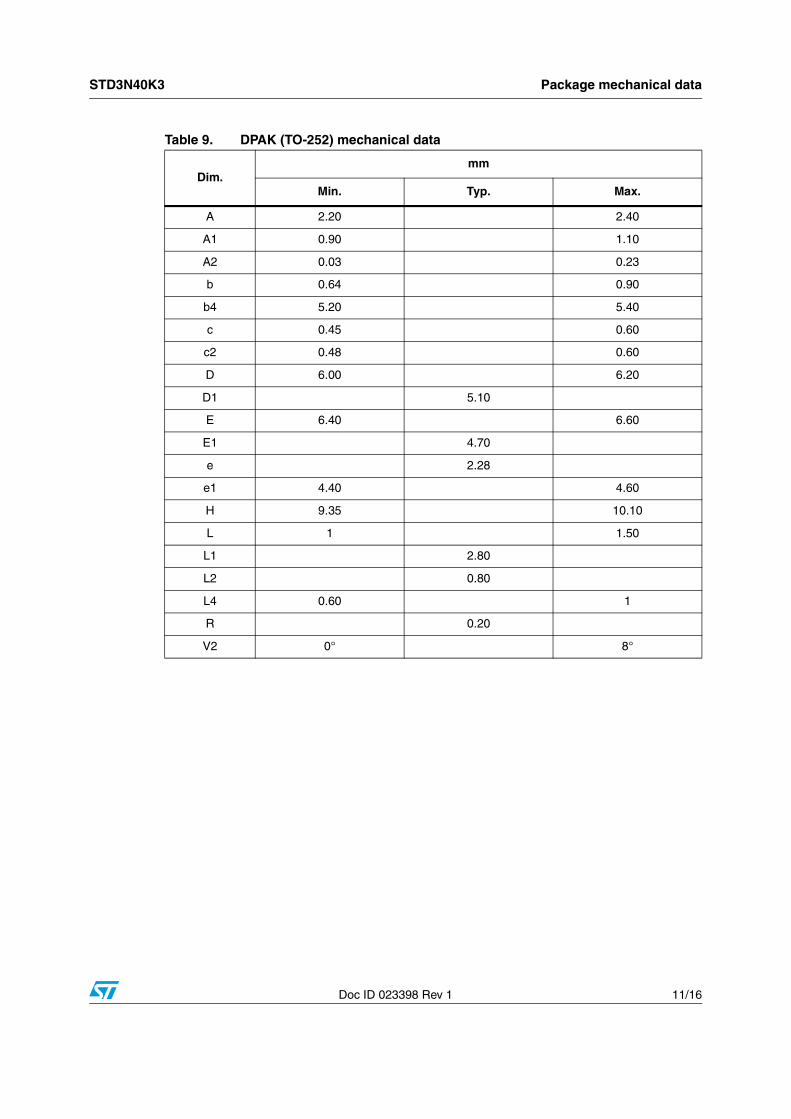
Figure 21. DPAK (TO-252) drawing
Figure 22. DPAK footprint(a)
a. All dimension are in millimeters
0068772_I
6.7
1.6
1.6
2.3
2.3
6.7 1.8 3
AM08850v1
STD3N40K3 Packaging mechanical data
Doc ID 023398 Rev 1 13/16
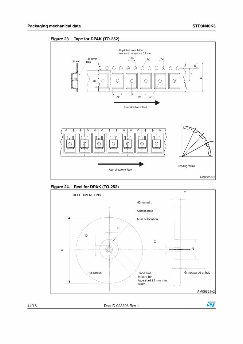
5 Packaging mechanical data
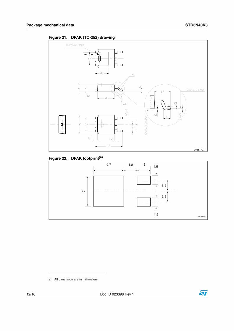
Table 10. DPAK (TO-252) tape and reel mechanical data
Tape Reel
Dim.mm
Dim.mm
Min. Max. Min. Max.
A0 6.8 7 A 330
B0 10.4 10.6 B 1.5
B1 12.1 C 12.8 13.2
D 1.5 1.6 D 20.2
D1 1.5 G 16.4 18.4
E 1.65 1.85 N 50
F 7.4 7.6 T 22.4
K0 2.55 2.75
P0 3.9 4.1 Base qty. 2500
P1 7.9 8.1 Bulk qty. 2500
P2 1.9 2.1
R 40
T 0.25 0.35
W 15.7 16.3
Packaging mechanical data STD3N40K3
14/16 Doc ID 023398 Rev 1
Figure 23. Tape for DPAK (TO-252)
Figure 24. Reel for DPAK (TO-252)
P1A0 D1
P0
F
W
E
D
B0K0
T
User direction of feed
P2
10 pitches cumulativetolerance on tape +/- 0.2 mm
User direction of feed
R
Bending radius
Top covertape
AM08852v2
A
D
B
Full radius G measured at hub
C
N
REEL DIMENSIONS
40mm min.
Access hole
At sl ot location
T
Tape slot in core fortape start 25 mm min.width
AM08851v2
STD3N40K3 Revision history
Doc ID 023398 Rev 1 15/16
6 Revision history
Table 11. Document revision history
Date Revision Changes
24-Jul-2012 1 First release.
STD3N40K3
16/16 Doc ID 023398 Rev 1
Please Read Carefully:
Information in this document is provided solely in connection with ST products. STMicroelectronics NV and its subsidiaries (“ST”) reserve theright to make changes, corrections, modifications or improvements, to this document, and the products and services described herein at anytime, without notice.
All ST products are sold pursuant to ST’s terms and conditions of sale.
Purchasers are solely responsible for the choice, selection and use of the ST products and services described herein, and ST assumes noliability whatsoever relating to the choice, selection or use of the ST products and services described herein.
No license, express or implied, by estoppel or otherwise, to any intellectual property rights is granted under this document. If any part of thisdocument refers to any third party products or services it shall not be deemed a license grant by ST for the use of such third party productsor services, or any intellectual property contained therein or considered as a warranty covering the use in any manner whatsoever of suchthird party products or services or any intellectual property contained therein.
UNLESS OTHERWISE SET FORTH IN ST’S TERMS AND CONDITIONS OF SALE ST DISCLAIMS ANY EXPRESS OR IMPLIEDWARRANTY WITH RESPECT TO THE USE AND/OR SALE OF ST PRODUCTS INCLUDING WITHOUT LIMITATION IMPLIEDWARRANTIES OF MERCHANTABILITY, FITNESS FOR A PARTICULAR PURPOSE (AND THEIR EQUIVALENTS UNDER THE LAWSOF ANY JURISDICTION), OR INFRINGEMENT OF ANY PATENT, COPYRIGHT OR OTHER INTELLECTUAL PROPERTY RIGHT.
UNLESS EXPRESSLY APPROVED IN WRITING BY TWO AUTHORIZED ST REPRESENTATIVES, ST PRODUCTS ARE NOTRECOMMENDED, AUTHORIZED OR WARRANTED FOR USE IN MILITARY, AIR CRAFT, SPACE, LIFE SAVING, OR LIFE SUSTAININGAPPLICATIONS, NOR IN PRODUCTS OR SYSTEMS WHERE FAILURE OR MALFUNCTION MAY RESULT IN PERSONAL INJURY,DEATH, OR SEVERE PROPERTY OR ENVIRONMENTAL DAMAGE. ST PRODUCTS WHICH ARE NOT SPECIFIED AS "AUTOMOTIVEGRADE" MAY ONLY BE USED IN AUTOMOTIVE APPLICATIONS AT USER’S OWN RISK.
Resale of ST products with provisions different from the statements and/or technical features set forth in this document shall immediately voidany warranty granted by ST for the ST product or service described herein and shall not create or extend in any manner whatsoever, anyliability of ST.
ST and the ST logo are trademarks or registered trademarks of ST in various countries.
Information in this document supersedes and replaces all information previously supplied.
The ST logo is a registered trademark of STMicroelectronics. All other names are the property of their respective owners.
© 2012 STMicroelectronics - All rights reserved
STMicroelectronics group of companies
Australia - Belgium - Brazil - Canada - China - Czech Republic - Finland - France - Germany - Hong Kong - India - Israel - Italy - Japan - Malaysia - Malta - Morocco - Philippines - Singapore - Spain - Sweden - Switzerland - United Kingdom - United States of America
www.st.com