N-channel 600 V, 13 typ., 0.3 A Zener-protected … · IAR Avalanche current, repetitive or not...
18
This is information on a product in full production. July 2014 DocID9509 Rev 14 1/18 STN1NK60Z, STQ1NK60ZR N-channel 600 V, 13 Ω typ., 0.3 A Zener-protected SuperMESH™ Power MOSFETs in SOT-223 and TO-92 packages Datasheet - production data Figure 1. Internal schematic diagram Features • 100% avalanche tested • Extremely high dv/dt capability • Gate charge minimized • ESD improved capability • Zener-protected Applications • Switching applications Description These devices are N-channel Zener-protected Power MOSFETs developed using STMicroelectronics' SuperMESH™ technology, achieved through optimization of ST's well established strip-based PowerMESH™ layout. In addition to a significant reduction in on- resistance, this device is designed to ensure a high level of dv/dt capability for the most demanding applications. 1 2 4 3 TO-92 (Ammopak) SOT-223 D(2,4) G(1) S(3) AM01476v1 Order codes V DS R DS(on)max I D P TOT STN1NK60Z 600 V 15 Ω 0.3 A 3.3 W STQ1NK60ZR-AP 3 W Table 1. Device summary Order codes Marking Package Packaging STN1NK60Z 1NK60Z SOT-223 Tape and reel STQ1NK60ZR-AP 1NK60ZR TO-92 Ammopak www.st.com
Transcript of N-channel 600 V, 13 typ., 0.3 A Zener-protected … · IAR Avalanche current, repetitive or not...
This is information on a product in full production.
July 2014 DocID9509 Rev 14 1/18
STN1NK60Z, STQ1NK60ZR
N-channel 600 V, 13 Ω typ., 0.3 A Zener-protected SuperMESH™ Power MOSFETs in SOT-223 and TO-92 packages
Datasheet - production data
Figure 1. Internal schematic diagram
Features
• 100% avalanche tested
• Extremely high dv/dt capability
• Gate charge minimized
• ESD improved capability
• Zener-protected
Applications• Switching applications
DescriptionThese devices are N-channel Zener-protected Power MOSFETs developed using STMicroelectronics' SuperMESH™ technology, achieved through optimization of ST's well established strip-based PowerMESH™ layout. In addition to a significant reduction in on-resistance, this device is designed to ensure a high level of dv/dt capability for the most demanding applications.
12
4
3
TO-92 (Ammopak)SOT-223
D(2,4)
G(1)
S(3)AM01476v1
Order codes VDS RDS(on)max ID PTOT
STN1NK60Z600 V 15 Ω 0.3 A
3.3 W
STQ1NK60ZR-AP 3 W
Table 1. Device summary
Order codes Marking Package Packaging
STN1NK60Z 1NK60Z SOT-223 Tape and reel
STQ1NK60ZR-AP 1NK60ZR TO-92 Ammopak
www.st.com

Contents STN1NK60Z, STQ1NK60ZR
2/18 DocID9509 Rev 14
Contents
1 Electrical ratings . . . . . . . . . . . . . . . . . . . . . . . . . . . . . . . . . . . . . . . . . . . . 3
2 Electrical characteristics . . . . . . . . . . . . . . . . . . . . . . . . . . . . . . . . . . . . . 4
2.1 Electrical characteristics (curves) . . . . . . . . . . . . . . . . . . . . . . . . . . . . . . . . 6
3 Test circuits . . . . . . . . . . . . . . . . . . . . . . . . . . . . . . . . . . . . . . . . . . . . . . 9
4 Package mechanical data . . . . . . . . . . . . . . . . . . . . . . . . . . . . . . . . . . . . 10
4.1 SOT-223, STN1NK60Z . . . . . . . . . . . . . . . . . . . . . . . . . . . . . . . . . . . . . . . .11
4.2 TO-92 ammopack, STQ1NK60ZR-AP . . . . . . . . . . . . . . . . . . . . . . . . . . . 13
5 Packaging mechanical data . . . . . . . . . . . . . . . . . . . . . . . . . . . . . . . . . . 15
6 Revision history . . . . . . . . . . . . . . . . . . . . . . . . . . . . . . . . . . . . . . . . . . . 17
DocID9509 Rev 14 3/18
STN1NK60Z, STQ1NK60ZR Electrical ratings
18
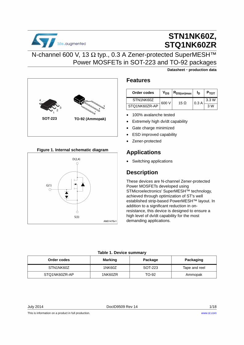
1 Electrical ratings
Table 2. Absolute maximum ratings
Symbol ParameterValue
UnitSOT-223 TO-92
VDS Drain-source voltage 600 V
VGS Gate-source voltage ± 30 V
ID Drain current (continuous) at TC = 25 °C 0.3 A
ID Drain current (continuous) at TC=100 °C 0.189 A
IDM(1)
1. Pulse width limited by safe operating area
Drain current (pulsed) 1.2 A
PTOT Total dissipation at TC = 25 °C 3.3 3 W
Derating factor 0.026 0.024 W/°C
ESDHuman body modelC=100 pF, R=1.5 kΩ 800 V
dv/dt(2)
2. ISD ≤ 0.3 A, di/dt ≤ 200 A/µs, VDD = 80%V(BR)DSS
Peak diode recovery voltage slope 4.5 V/ns
TJ Operating junction temperature- 55 to 150
°C
Tstg Storage temperature °C
Table 3. Thermal resistance
Symbol ParameterValue
UnitSOT-223 TO-92
Rthj-amb Thermal resistance junction-ambient max 38(1)
1. When mounted on 1 inch² FR-4 board, 2 Oz Cu, t < 30 s.
120 °C/W
Rthj-lead Thermal resistance junction-lead max 40 °C/W
Table 4. Avalanche data
Symbol Parameter Value Unit
IARAvalanche current, repetitive or not repetitive
(pulse width limited by Tj max)0.3 A
EASSingle pulse avalanche energy
(starting TJ = 25 °C, ID = IAR, VDD = 50 V)60 mJ

Electrical characteristics STN1NK60Z, STQ1NK60ZR
4/18 DocID9509 Rev 14
2 Electrical characteristics
(TCASE = 25 °C unless otherwise specified)
Table 5. On/off states
Symbol Parameter Test conditions Min. Typ. Max. Unit
V(BR)DSSDrain-source breakdown voltage
VGS= 0, ID = 1 mA 600 V
IDSSZero gate voltage drain current
VGS = 0, VDS =600 V 1 µA
VGS = 0, VDS =600 V, TC = 125 °C
50 µA
IGSS Gate body leakage current VDS = 0, VGS = ± 20 V ±10 µA
VGS(th) Gate threshold voltage VDS = VGS, ID = 50 µA 3 3.75 4.5 V
RDS(on)Static drain-source on- resistance
VGS = 10 V, ID = 0.4 A 13 15 Ω
Table 6. Dynamic
Symbol Parameter Test conditions Min. Typ. Max. Unit
gfs (1)
1. Pulsed: pulse duration=300µs, duty cycle 1.5%
Forward transconductance VDS =15 V, ID = 0.4 A - 0.5 S
Ciss Input capacitance
VGS = 0, VDS = 25 V, f=1 MHz
- 94 pF
Coss Output capacitance - 17.6 pF
CrssReverse transfer capacitance
- 2.8 pF
Coss eq(2)
.
2. Coss eq. is defined as a constant equivalent capacitance giving the same charging time as Coss when VDS increases from 0 to 80% VDSS
Equivalent output capacitance
VGS= 0, VDS = 0 to 480 V - 11 pF
Qg Total gate charge VDD=480 V, ID = 0.8 A
VGS =10 V
(see Figure 19)
- 4.9 6.9 nC
Qgs Gate-source charge - 1 nC
Qgd Gate-drain charge - 2.7 nC

DocID9509 Rev 14 5/18
STN1NK60Z, STQ1NK60ZR Electrical characteristics
18
The built-in back-to-back Zener diodes have specifically been designed to enhance the device's ESD capability. In this respect the Zener voltage is appropriate to achieve an efficient and cost-effective intervention to protect the device's integrity. These integrated Zener diodes thus avoid the usage of external components.
Table 7. Switching times
Symbol Parameter Test conditions Min. Typ. Max. Unit
td(on) Turn-on delay time
VDD = 300 V, ID = 0.4 A,
RG = 4.7 Ω, VGS = 10 V
(see Figure 18)
- 5.5 - ns
tr Rise time - 5 - ns
td(off) Turn-off delay time - 13 - ns
tf Fall time - 28 - ns
Table 8. Source drain diode
Symbol Parameter Test conditions Min. Typ. Max. Unit
ISD Source-drain current - 0.8 A
ISDM(1)
1. Pulse width limited by safe operating area.
Source-drain current (pulsed) - 2.4 A
VSD(2)
2. Pulsed: pulse duration=300µs, duty cycle 1.5%
Forward on voltage VGS=0, ISD = 0.8 A - 1.6 V
trr Reverse recovery time ISD = 0.8 A,
di/dt = 100 A/µs,VDD = 20 V
- 135 ns
Qrr Reverse recovery charge - 216 nC
IRRM Reverse recovery current - 3.2 A
trr Reverse recovery time ISD = 0.8 A,
di/dt = 100 A/µs,VDD = 20V, Tj = 150 °C
- 140 ns
Qrr Reverse recovery charge - 224 nC
IRRM Reverse recovery current - 3.2 A
Table 9. Gate-source Zener diode
Symbol Parameter Test conditions Min Typ. Max. Unit
V(BR)GSO Gate-source breakdown voltage IGS = ± 1mA, ID=0 30 - - V

Electrical characteristics STN1NK60Z, STQ1NK60ZR
6/18 DocID9509 Rev 14
2.1 Electrical characteristics (curves)
Figure 2. Safe operating area for SOT-223 Figure 3. Thermal impedance for SOT-223
10-3
10-2
10-1 10
010
1tp(s)
10-2
10-1
K
0.2
0.05
0.02
0.01
0.1
Zthj-pcb=K*Rthj-pcb, Rthj-pcb=62.5°C/W
Single pulse
δ=0.5
102
t < 30s
SOT-223
Figure 4. Safe operating area for TO-92 Figure 5. Thermal impedance for TO-92
Figure 6. Output characteristics Figure 7. Transfer characteristics

DocID9509 Rev 14 7/18
STN1NK60Z, STQ1NK60ZR Electrical characteristics
18
Figure 8. Transconductance Figure 9. Static drain-source on-resistance
Figure 10. Gate charge vs gate-source voltage Figure 11. Capacitance variations
Figure 12. Normalized gate threshold voltage vs temperature
Figure 13. Normalized on-resistance vs temperature

Electrical characteristics STN1NK60Z, STQ1NK60ZR
8/18 DocID9509 Rev 14
Figure 14. Source-drain diode forward characteristics
Figure 15. Normalized VBR(DSS) vs temperature
Figure 16. Maximum avalanche energy vs temperature
Figure 17. Max Id current vs Tc
BR(DSS)
DocID9509 Rev 14 9/18
STN1NK60Z, STQ1NK60ZR Test circuits
18
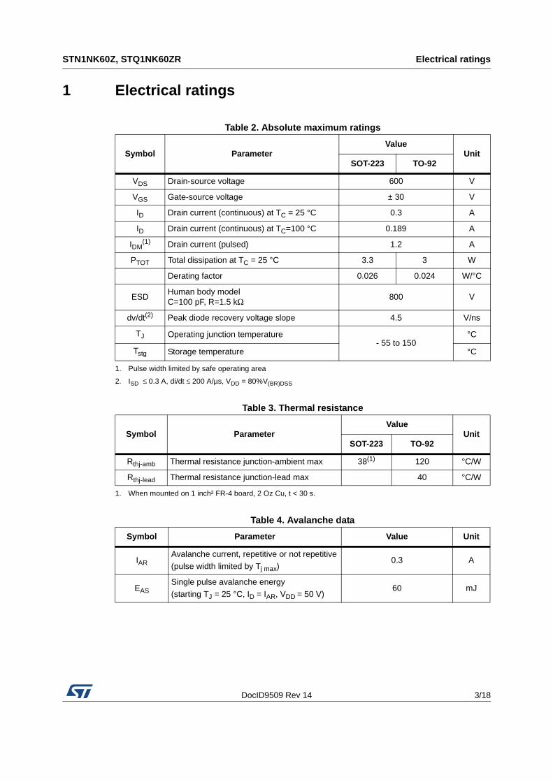
3 Test circuits
Figure 18. Switching times test circuit for resistive load
Figure 19. Gate charge test circuit
Figure 20. Test circuit for inductive load switching and diode recovery times
Figure 21. Unclamped inductive load test circuit
Figure 22. Unclamped inductive waveform Figure 23. Switching time waveform
AM01468v1
VGS
PW
VD
RG
RL
D.U.T.
2200
μF3.3μF
VDD
AM01469v1
VDD
47kΩ 1kΩ
47kΩ
2.7kΩ
1kΩ
12V
Vi=20V=VGMAX
2200μF
PW
IG=CONST100Ω
100nF
D.U.T.
VG
AM01470v1
AD
D.U.T.
SB
G
25 Ω
A A
BB
RG
G
FASTDIODE
D
S
L=100μH
μF3.3 1000
μF VDD
AM01471v1
Vi
Pw
VD
ID
D.U.T.
L
2200μF
3.3μF VDD
AM01472v1
V(BR)DSS
VDDVDD
VD
IDM
ID
AM01473v1
VDS
ton
tdon tdoff
toff
tftr
90%
10%
10%
0
0
90%
90%
10%
VGS

Package mechanical data STN1NK60Z, STQ1NK60ZR
10/18 DocID9509 Rev 14
4 Package mechanical data
In order to meet environmental requirements, ST offers these devices in different grades of ECOPACK® packages, depending on their level of environmental compliance. ECOPACK® specifications, grade definitions and product status are available at: www.st.com. ECOPACK® is an ST trademark.

DocID9509 Rev 14 11/18
STN1NK60Z, STQ1NK60ZR Package mechanical data
18
Figure 24. SOT-223 mechanical data drawing
Table 10. SOT-223 mechanical data
Dim.mm
Min. Typ. Max.
A 1.80
A1 0.02 0.10
B 0.60 0.70 0.85
B1 2.9 3.0 3.15
c 0.24 0.26 0.35
D 6.30 6.50 6.70
e 2.30 6.70
e1 4.60
E 3.30 3.50 3.70
H 6.70 7.0 7.30
V 10°
0046067_N

Package mechanical data STN1NK60Z, STQ1NK60ZR
12/18 DocID9509 Rev 14
Figure 25. SOT-223 footprint (dimensions in mm)
0046067_N_footprint

DocID9509 Rev 14 13/18
STN1NK60Z, STQ1NK60ZR Package mechanical data
18
4.1 SOT-223, STN1NK60Z
4.2 TO-92 ammopack, STQ1NK60ZR-AP
Figure 26. TO-92 ammopack mechanical data drawing
WW1
W0
W2
A1
d
D0
H1
HH0
L
l1
F1 F2
P2P0
delta H
T2 T1T
tF3
H3
0050910S_Rev_U

Package mechanical data STN1NK60Z, STQ1NK60ZR
14/18 DocID9509 Rev 14
Table 11. TO-92 ammopack mechanical data
Dim.mm
Min. Typ. Max.
A1 4.80
T 3.80
T1 1.60
T2 2.30
d 0.45 0.47 0.48
P0 12.50 12.70 12.90
P2 5.65 6.35 7.05
F1, F2 2.40 2.50 2.94
F3 4.98 5.08 5.48
delta H -2.00 2.00
W 17.50 18.00 19.00
W0 5.5 6.00 6.5
W1 8.50 9.00 9.25
W2 0.50
H 18.50 21
H3 0.5 1 2
H0 15.50 16.00 18.8
H1 25.0 27.0
D0 3.80 4.00 4.20
t 0.90
L 11.00
l1 3.00
delta P -1.00 1.00
DocID9509 Rev 14 15/18
STN1NK60Z, STQ1NK60ZR Packaging mechanical data
18
5 Packaging mechanical data
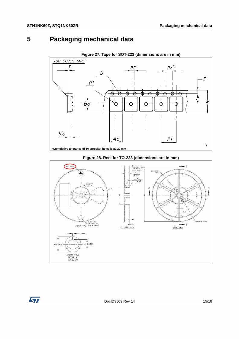
Figure 27. Tape for SOT-223 (dimensions are in mm)
Figure 28. Reel for TO-223 (dimensions are in mm)
*Cumulative tolerance of 10 sprocket holes is ±0.20 mm

Packaging mechanical data STN1NK60Z, STQ1NK60ZR
16/18 DocID9509 Rev 14
Table 12. SOT-223 tape and reel mechanical data
Tape Reel
Dim.mm
Dim.mm
Min. Typ. Max. Min. Max.
A0 6.75 6.85 6.95 A 180
B0 7.30 7.40 7.50 N 60
K0 1.80 1.90 2.00 W1 12.4
F 5.40 5.50 5.60 W2 18.4
E 1.65 1.75 1.85 W3 11.9 15.4
W 11.7 12 12.3
P2 1.90 2 2.10 Base quantity pcs 1000
P0 3.90 4 4.10 Bulk quantity pcs 1000
P1 7.90 8 8.10
T 0.25 0.30 0.35
Dφ 1.50 1.55 1.60
D1φ 1.50 1.60 1.70

DocID9509 Rev 14 17/18
STN1NK60Z, STQ1NK60ZR Revision history
18
6 Revision history
Table 13. Revision history
Date Revision Changes
19-Mar-2003 3 First electronic version
15-May-2003 4 Removed DPAK
09-Jun-2003 5 Final datasheet
17-Nov-2004 6 Inserted SOT-223
15-Feb-2005 7 Modified Figure 4.
07-Sep-2005 8 Inserted ecopack indication
22-Feb-2006 9 The document has been reformatted
01-Jun-2007 10 Order code table on first page has been updated
19-Jul-2007 11 Table 1: Device summary has been updated
05-Jan-2011 12Corrected Figure 2: Safe operating area for SOT-223 and Figure 3: Thermal impedance for SOT-223
05-Jun-2014 13
– Updated title.
– Updated derating factor in Table 2: Absolute maximum ratings.– Updated Section 4: Package mechanical data.– Minor text changes.
04-Jul-2014 14 – Updated Section 3: Test circuits.

STN1NK60Z, STQ1NK60ZR
18/18 DocID9509 Rev 14
Please Read Carefully:
Information in this document is provided solely in connection with ST products. STMicroelectronics NV and its subsidiaries (“ST”) reserve theright to make changes, corrections, modifications or improvements, to this document, and the products and services described herein at anytime, without notice.
All ST products are sold pursuant to ST’s terms and conditions of sale.
Purchasers are solely responsible for the choice, selection and use of the ST products and services described herein, and ST assumes noliability whatsoever relating to the choice, selection or use of the ST products and services described herein.
No license, express or implied, by estoppel or otherwise, to any intellectual property rights is granted under this document. If any part of thisdocument refers to any third party products or services it shall not be deemed a license grant by ST for the use of such third party productsor services, or any intellectual property contained therein or considered as a warranty covering the use in any manner whatsoever of suchthird party products or services or any intellectual property contained therein.
UNLESS OTHERWISE SET FORTH IN ST’S TERMS AND CONDITIONS OF SALE ST DISCLAIMS ANY EXPRESS OR IMPLIEDWARRANTY WITH RESPECT TO THE USE AND/OR SALE OF ST PRODUCTS INCLUDING WITHOUT LIMITATION IMPLIEDWARRANTIES OF MERCHANTABILITY, FITNESS FOR A PARTICULAR PURPOSE (AND THEIR EQUIVALENTS UNDER THE LAWSOF ANY JURISDICTION), OR INFRINGEMENT OF ANY PATENT, COPYRIGHT OR OTHER INTELLECTUAL PROPERTY RIGHT.
ST PRODUCTS ARE NOT DESIGNED OR AUTHORIZED FOR USE IN: (A) SAFETY CRITICAL APPLICATIONS SUCH AS LIFESUPPORTING, ACTIVE IMPLANTED DEVICES OR SYSTEMS WITH PRODUCT FUNCTIONAL SAFETY REQUIREMENTS; (B)AERONAUTIC APPLICATIONS; (C) AUTOMOTIVE APPLICATIONS OR ENVIRONMENTS, AND/OR (D) AEROSPACE APPLICATIONSOR ENVIRONMENTS. WHERE ST PRODUCTS ARE NOT DESIGNED FOR SUCH USE, THE PURCHASER SHALL USE PRODUCTS ATPURCHASER’S SOLE RISK, EVEN IF ST HAS BEEN INFORMED IN WRITING OF SUCH USAGE, UNLESS A PRODUCT ISEXPRESSLY DESIGNATED BY ST AS BEING INTENDED FOR “AUTOMOTIVE, AUTOMOTIVE SAFETY OR MEDICAL” INDUSTRYDOMAINS ACCORDING TO ST PRODUCT DESIGN SPECIFICATIONS. PRODUCTS FORMALLY ESCC, QML OR JAN QUALIFIED AREDEEMED SUITABLE FOR USE IN AEROSPACE BY THE CORRESPONDING GOVERNMENTAL AGENCY.
Resale of ST products with provisions different from the statements and/or technical features set forth in this document shall immediately voidany warranty granted by ST for the ST product or service described herein and shall not create or extend in any manner whatsoever, anyliability of ST.
ST and the ST logo are trademarks or registered trademarks of ST in various countries.Information in this document supersedes and replaces all information previously supplied.
The ST logo is a registered trademark of STMicroelectronics. All other names are the property of their respective owners.
© 2014 STMicroelectronics - All rights reserved
STMicroelectronics group of companies
Australia - Belgium - Brazil - Canada - China - Czech Republic - Finland - France - Germany - Hong Kong - India - Israel - Italy - Japan - Malaysia - Malta - Morocco - Philippines - Singapore - Spain - Sweden - Switzerland - United Kingdom - United States of America
www.st.com


![γδ TCellsAreRequiredforM2Macrophage ... · subacute O 3 exposure(0.3 ppmfor72h)[8],thoughsome effects ofO 3 persisteven 72hafter amoreprolonged exposure [9].While theprocessespromotingO](https://static.fdocument.org/doc/165x107/5f292d95a054f528ee0de564/-tcellsarerequiredform2macrophage-subacute-o-3-exposure03-ppmfor72h8thoughsome.jpg)