MZ-E707 - Minidisc
32
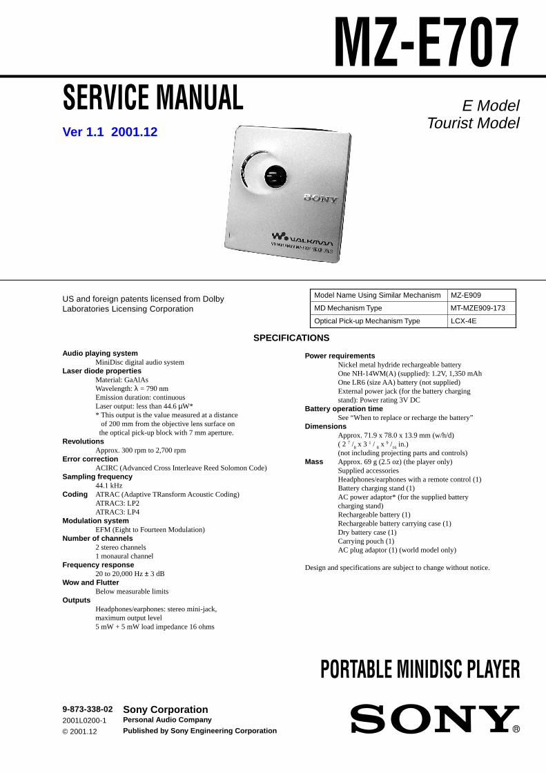
MZ-E707 SERVICE MANUAL PORTABLE MINIDISC PLAYER SPECIFICATIONS E Model Tourist Model Model Name Using Similar Mechanism MZ-E909 MD Mechanism Type MT-MZE909-173 Optical Pick-up Mechanism Type LCX-4E US and foreign patents licensed from Dolby Laboratories Licensing Corporation Ver 1.1 2001.12 9-873-338-02 2001L0200-1 © 2001.12 Sony Corporation Personal Audio Company Published by Sony Engineering Corporation Audio playing system MiniDisc digital audio system Laser diode properties Material: GaAlAs Wavelength: λ = 790 nm Emission duration: continuous Laser output: less than 44.6 µW* * This output is the value measured at a distance of 200 mm from the objective lens surface on the optical pick-up block with 7 mm aperture. Revolutions Approx. 300 rpm to 2,700 rpm Error correction ACIRC (Advanced Cross Interleave Reed Solomon Code) Sampling frequency 44.1 kHz Coding ATRAC (Adaptive TRansform Acoustic Coding) ATRAC3: LP2 ATRAC3: LP4 Modulation system EFM (Eight to Fourteen Modulation) Number of channels 2 stereo channels 1 monaural channel Frequency response 20 to 20,000 Hz ± 3 dB Wow and Flutter Below measurable limits Outputs Headphones/earphones: stereo mini-jack, maximum output level 5 mW + 5 mW load impedance 16 ohms Power requirements Nickel metal hydride rechargeable battery One NH-14WM(A) (supplied): 1.2V, 1,350 mAh One LR6 (size AA) battery (not supplied) External power jack (for the battery charging stand): Power rating 3V DC Battery operation time See “When to replace or recharge the battery” Dimensions Approx. 71.9 x 78.0 x 13.9 mm (w/h/d) ( 2 7 / 8 x 3 1 / 8 x 9 / 16 in.) (not including projecting parts and controls) Mass Approx. 69 g (2.5 oz) (the player only) Supplied accessories Headphones/earphones with a remote control (1) Battery charging stand (1) AC power adaptor* (for the supplied battery charging stand) Rechargeable battery (1) Rechargeable battery carrying case (1) Dry battery case (1) Carrying pouch (1) AC plug adaptor (1) (world model only) Design and specifications are subject to change without notice.
Transcript of MZ-E707 - Minidisc
MZ-E707SERVICE MANUAL
PORTABLE MINIDISC PLAYER
SPECIFICATIONS
E ModelTourist Model
Model Name Using Similar Mechanism MZ-E909
MD Mechanism Type MT-MZE909-173
Optical Pick-up Mechanism Type LCX-4E
US and foreign patents licensed from DolbyLaboratories Licensing Corporation
Ver 1.1 2001.12
9-873-338-022001L0200-1
© 2001.12
Sony CorporationPersonal Audio Company
Published by Sony Engineering Corporation
Audio playing systemMiniDisc digital audio system
Laser diode propertiesMaterial: GaAlAsWavelength: λ = 790 nmEmission duration: continuousLaser output: less than 44.6 µW** This output is the value measured at a distance of 200 mm from the objective lens surface on the optical pick-up block with 7 mm aperture.
RevolutionsApprox. 300 rpm to 2,700 rpm
Error correctionACIRC (Advanced Cross Interleave Reed Solomon Code)
Sampling frequency44.1 kHz
Coding ATRAC (Adaptive TRansform Acoustic Coding)ATRAC3: LP2ATRAC3: LP4
Modulation systemEFM (Eight to Fourteen Modulation)
Number of channels2 stereo channels1 monaural channel
Frequency response20 to 20,000 Hz ± 3 dB
Wow and FlutterBelow measurable limits
OutputsHeadphones/earphones: stereo mini-jack,maximum output level5 mW + 5 mW load impedance 16 ohms
Power requirementsNickel metal hydride rechargeable batteryOne NH-14WM(A) (supplied): 1.2V, 1,350 mAhOne LR6 (size AA) battery (not supplied)External power jack (for the battery chargingstand): Power rating 3V DC
Battery operation timeSee “When to replace or recharge the battery”
DimensionsApprox. 71.9 x 78.0 x 13.9 mm (w/h/d)( 2 7 /
8 x 3 1 /
8 x 9 /
16 in.)
(not including projecting parts and controls)Mass Approx. 69 g (2.5 oz) (the player only)
Supplied accessoriesHeadphones/earphones with a remote control (1)Battery charging stand (1)AC power adaptor* (for the supplied batterycharging stand)Rechargeable battery (1)Rechargeable battery carrying case (1)Dry battery case (1)Carrying pouch (1)AC plug adaptor (1) (world model only)
Design and specifications are subject to change without notice.
2
MZ-E707Ver 1.1 2001.12
Specifications ........................................................................... 1
1. SERVICING NOTE ...................................................... 3
2. GENERALPlaying an MD ................................................................... 4
3. DISASSEMBLY3-1. Upper Lid ASSY ......................................................... 53-2. Mechanism ASSY ...................................................... 53-3. Bracket (R) ASSY ...................................................... 63-4. Main Board Sub ASSY, SW Board ............................. 63-5. Optical Pick-up ASSY ................................................ 7
4. TEST MODE .................................................................. 8
5. ELECTRICAL ADJUSTMENTS ........................... 12
6. DIAGRAMS6-1. Explanation of IC Terminals ..................................... 166-2. Block Diagram .......................................................... 176-3. Printed Wiring Boards – Main Section (1/2) – ......... 186-4. Printed Wiring Boards – Main Section (2/2) – ......... 196-5. Schematic Diagram – Main Section (1/2) – ............. 206-6. Schematic Diagram – Main Section (2/2) – ............. 216-7. Printed Wiring Boards – Audio Section – ................ 226-8. Schematic Diagram – Audio Section – ..................... 23
7. EXPLODED VIEWS7-1. Main Section ............................................................. 277-2. Mechanism Deck Section ......................................... 28
8. ELECTRICAL PARTS LIST ................................... 29
SAFETY-RELATED COMPONENT WARNING!!
COMPONENTS IDENTIFIED BY MARK ! OR DOTTED LINE WITHMARK ! ON THE SCHEMATIC DIAGRAMS AND IN THE PARTSLIST ARE CRITICAL TO SAFE OPERATION.REPLACE THESE COMPONENTS WITH SONY PARTS WHOSEPART NUMBERS APPEAR AS SHOWN IN THIS MANUAL OR INSUPPLEMENTS PUBLISHED BY SONY.
Flexible Circuit Board Repairing• Keep the temperature of the soldering iron around 270°C during
repairing.• Do not touch the soldering iron on the same conductor of the
circuit board (within 3 times).• Be careful not to apply force on the conductor when soldering or
unsoldering.
Notes on chip component replacement• Never reuse a disconnected chip component.• Notice that the minus side of a tantalum capacitor may be dam-
aged by heat.
TABLE OF CONTENTS
* Replacement of CXD2671B-206GA (IC601) used in this setrequires a special tool.
CAUTIONUse of controls or adjustments or performance of proceduresother than those specified herein may result in hazardousradiation exposure.
• UNLEADED SOLDERBoards requiring use of unleaded solder are printed with thelead-free mark (LF) indicating the solder contains no lead.(Caution: Some printed circuit boards may not come printedwith the lead free mark due to their particular size.)
: LEAD FREE MARK
Unleaded solder has the following characteristics.• Unleaded solder melts at a temperature about 40°C higher
than ordinary solder.Ordinary soldering irons can be used but the iron tip has tobe applied to the solder joint for a slightly longer time.Soldering irons using a temperature regulator should be setto about 350°C.Caution: The printed pattern (copper foil) may peel away ifthe heated tip is applied for too long, so be careful!
• Strong viscosityUnleaded solder is more viscous (sticky, less prone toflow) than ordinary solder so use caution not to let solderbridges occur such as on IC pins, etc.
• Usable with ordinary solderIt is best to use only unleaded solder but unleaded soldermay also be added to ordinary solder.
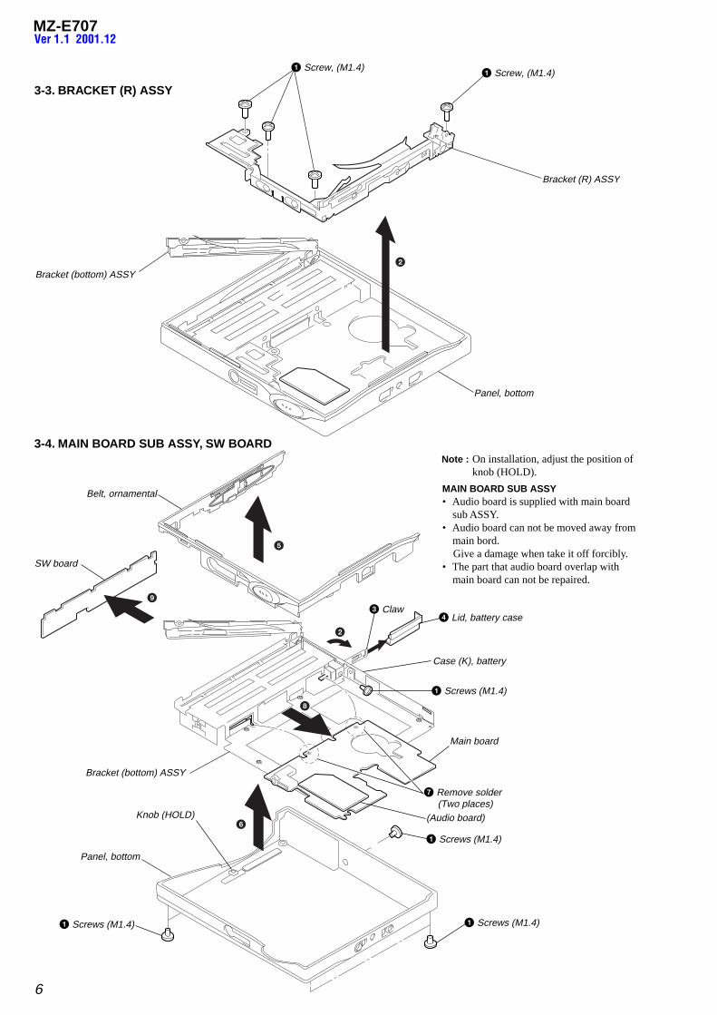
MAIN BOARD SUB ASSY• Audio board is supplied with main board sub ASSY.• Audio board can not be moved away from main bord.Give a damage when take it off forcibly.• The part that audio board overlap with main board can not be
repaired.
3
MZ-E707
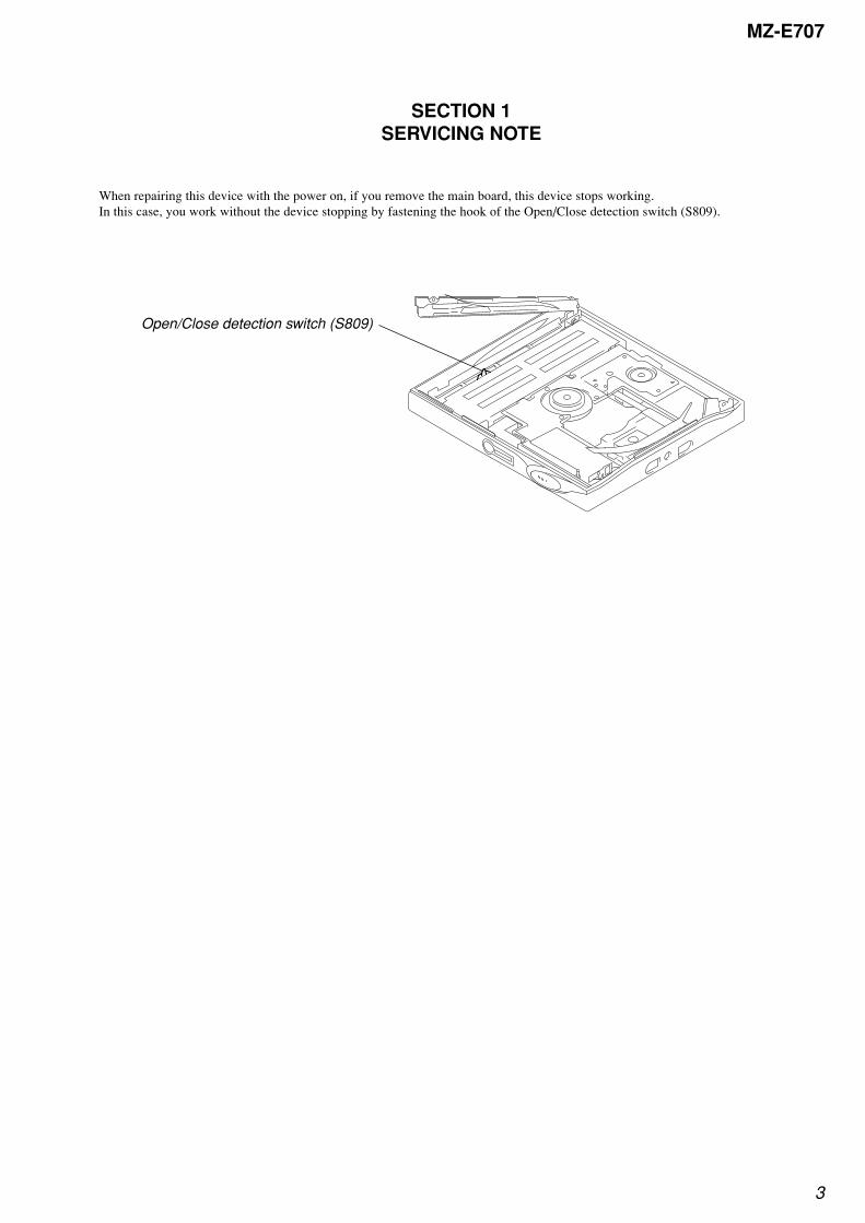
SECTION 1SERVICING NOTE
When repairing this device with the power on, if you remove the main board, this device stops working.In this case, you work without the device stopping by fastening the hook of the Open/Close detection switch (S809).
Open/Close detection switch (S809)
4
MZ-E707SECTION 2GENERAL
This section is extracted frominstruction manual.
The Player
1
9
7
F
E
C
D
2
8
1 ./x/> N button2 3 Color Info-LED3 GROUP button4 HOLD (Locking the control) switch5 i (earphones) jack6 OPEN switch7 Terminals for charging stand/
dry battery case (at the bottom)8 VOL +/– button9 Battery compartment
The earphones with a remotecontrol
J +–
HI
K
D
A
L
F
B
E
G
C
1 Headphones/earphones2 Stereo mini plug3 X (pause) button4 SOUND button5 RPT/ENT (Repeat/Enter) button6 PLAYMODE button7 DISPLAY button8 x (stop) button*9 Control (./N>)q; Control VOL +/–
Pull and turn to adjust the volume.qa HOLD (Locking the control) switchqs Display window
* The stop button also operates as the enterbutton, depending on the function.
The display window of the remotecontrol
F
G
A B CD E
1 Track number display2 Charactor information display3 Disc indication4 Alarm indication5 Play mode indication6 Battery level indication7 SOUND indication
The battery charging stand
B
AC
1 Terminals for charging2 CHARGE lamp3 DC IN (3V jack) (at the rear)
To
Find the beginning ofthe current track orthe previous track3)
Find the beginningof the next track4)
Go backwardswhile playing
Go forwardwhile playing
Pause
Remove the MD2) You can turn off the beep sound. For more details, see “Turning off the beep sound.”3) If you turn the control towards . on the remote control (or press . on the player) during the
first track of the disc, the player goes to the beginning of the last track on the disc.4) If you turn the control towards N> on the remote control (or press > N on the player) during
the last track of the disc, the player goes to the beginning of the first track on the disc.5) If you open the lid, the playback will begin from the beginning of the first track (except when disc
information is stored to the personal disc memory or when group mode is on).
zThe MZ-E707 supports the newly developed DSP TYPE-R for ATRAC.It thus allows you to enjoy TYPE-R high-quality sound from MDs recorded in SP stereo on TYPE-R-equipped MD decks, etc.
NoteWhen removing the disc, make sure to press x first, and then slide OPEN.
Viewing the display window of the remote control
Track number Track name6) or elapsed time of the track6) Appears only with MDs that have been electronically labeled.
z• The player can play the track recorded by 2 × or 4 × long playing mode (LP2 or LP4). Normal stereo
playback, LP2 stereo playback, LP4 stereo playback or monaural playback is automatically selected tomatch the audio source.
• The display on the remote control will turn off shortly after you press x.
Do this (Beeps2) in the headphones)
Turn the control towards . on the remote control once(three short beeps). (Or press . on the player once.)Turn the control towards . on the remote control repeatedly(continuous three short beeps). (Or press . on the playerrepeatedly.)
Turn the control towards N> on the remote control (twoshort beeps).Press > N on the player once.
Turn and hold the control towards . on the remote control.Hold down . on the player.
Turn and hold the control towards N> on the remote control.Hold down > N on the player.
Press X on the remote control (continuous short beeps).Press X on the remote control again to resume play.
Press x, and then slide OPEN.5)
Playing an MDInsert an MD.
1 2
3
Play an MD.2
> N
.
VOLUME +/–
GROUP
xx
X
1N>
VOL+
VOL–
.
1 Turn the control towards N> on the remote control (or press > N
on the player) to play the disc.A short beep sounds in the headphones/earphones when using the remote control.The LED flashes and then lights up.
2 Pull and turn VOL +/– on the remote control (or press VOLUME +/– on theplayer) to adjust the volume.The volume indicator appears in the display, allowing you to check thevolume level. After you adjust the volume, push back the control.
To stop play, press x.Playback starts from the point you last stopped playing. To start playback from thebeginning of the disc, turn and hold the control towards N> on the remote control(or hold down > N on the player) for 2 seconds or more.1) The LED indicates the current operating status by the lighting up in the following colors.
When the battery power is exhausted, the LED starts flashing. For more details, see“When to replace or recharge the battery.”
LED color Operating statusRed Normal play (The LED lights up continuously)Green Group mode* (The LED lights up continuously)Orange Group skip mode* (The LED lights for about 5 seconds)*For more details, see “Using the group function.”
1
2
Insert an MD with the lable side facing up, pushing theMD to the direction of the arrow in the illustration.
1 Slide OPEN to open the lid. 2 Insert an MD. 3 Close the lid.
3 Color Info-LED1)
5
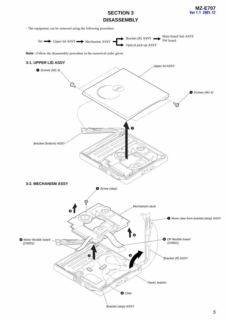
MZ-E707Ver 1.1 2001.12SECTION 3
DISASSEMBLY
Note : Follow the disassembly procedure in the numerical order given.
3-1. UPPER LID ASSY
3-2. MECHANISM ASSY
r The equipment can be removed using the following procedure.
Upper lid ASSYSetOptical pick-up ASSY
Mechsnism ASSYBracket (R) ASSY
Main board Sub ASSYSW board
2
1 Screws (M1.4)
1 Screws (M1.4)
Bracket (bottom) ASSY
Upper lid ASSY
7
5
2
4
9 Motor flexible board (CN551)
6 Claw
8 OP flexible board (CN501)
1 Move claw from bracket (stop) ASSY
3 Screw (step)
Bracket (stop) ASSY
Panel, bottom
Bracket (R) ASSY
Mechanism deck
6
MZ-E707Ver 1.1 2001.12
3-4. MAIN BOARD SUB ASSY, SW BOARDNote : On installation, adjust the position of
knob (HOLD).
3-3. BRACKET (R) ASSY
2
1 Screw, (M1.4)1 Screw, (M1.4)
Panel, bottom
Bracket (bottom) ASSY
Bracket (R) ASSY
6
8
9
5
2
Knob (HOLD)
Main board
Bracket (bottom) ASSY
SW board
Panel, bottom
7 Remove solder (Two places)
1 Screws (M1.4) 1 Screws (M1.4)
1 Screws (M1.4)
1 Screws (M1.4)
4 Lid, battery case
Case (K), battery
Belt, ornamental
3 Claw
(Audio board)
MAIN BOARD SUB ASSY• Audio board is supplied with main board
sub ASSY.• Audio board can not be moved away from
main bord. Give a damage when take it off forcibly.• The part that audio board overlap with
main board can not be repaired.
7
MZ-E707
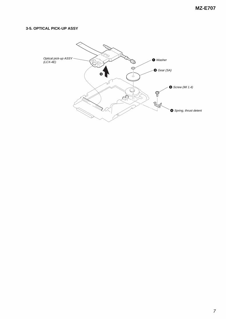
3-5. OPTICAL PICK-UP ASSY
5
3 Screw (MI 1.4)
4 Spring, thrust detent
1 Washer
2 Gear (SA)
Optical pick-up ASSY(LCX-4E)
8
MZ-E707
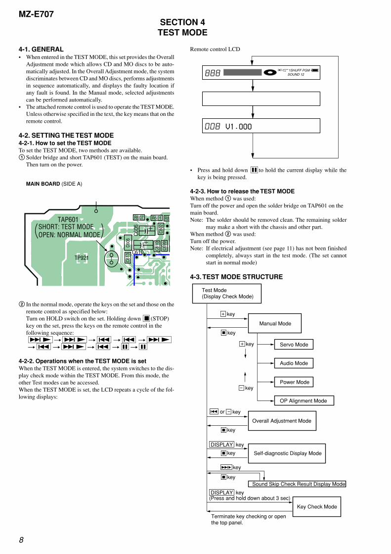
Remote control LCD
• Press and hold down X to hold the current display while thekey is being pressed.
4-2-3. How to release the TEST MODEWhen method 1 was used:Turn off the power and open the solder bridge on TAP601 on themain board.Note: The solder should be removed clean. The remaining solder
may make a short with the chassis and other part.When method 2 was used:Turn off the power.Note: If electrical adjustment (see page 11) has not been finished
completely, always start in the test mode. (The set cannotstart in normal mode)
4-3. TEST MODE STRUCTURE
4-1. GENERAL• When entered in the TEST MODE, this set provides the Overall
Adjustment mode which allows CD and MO discs to be auto-matically adjusted. In the Overall Adjustment mode, the systemdiscriminates between CD and MO discs, performs adjustmentsin sequence automatically, and displays the faulty location ifany fault is found. In the Manual mode, selected adjustmentscan be performed automatically.
• The attached remote control is used to operate the TEST MODE.Unless otherwise specified in the text, the key means that on theremote control.
4-2. SETTING THE TEST MODE4-2-1. How to set the TEST MODETo set the TEST MODE, two methods are available.1 Solder bridge and short TAP601 (TEST) on the main board.
Then turn on the power.
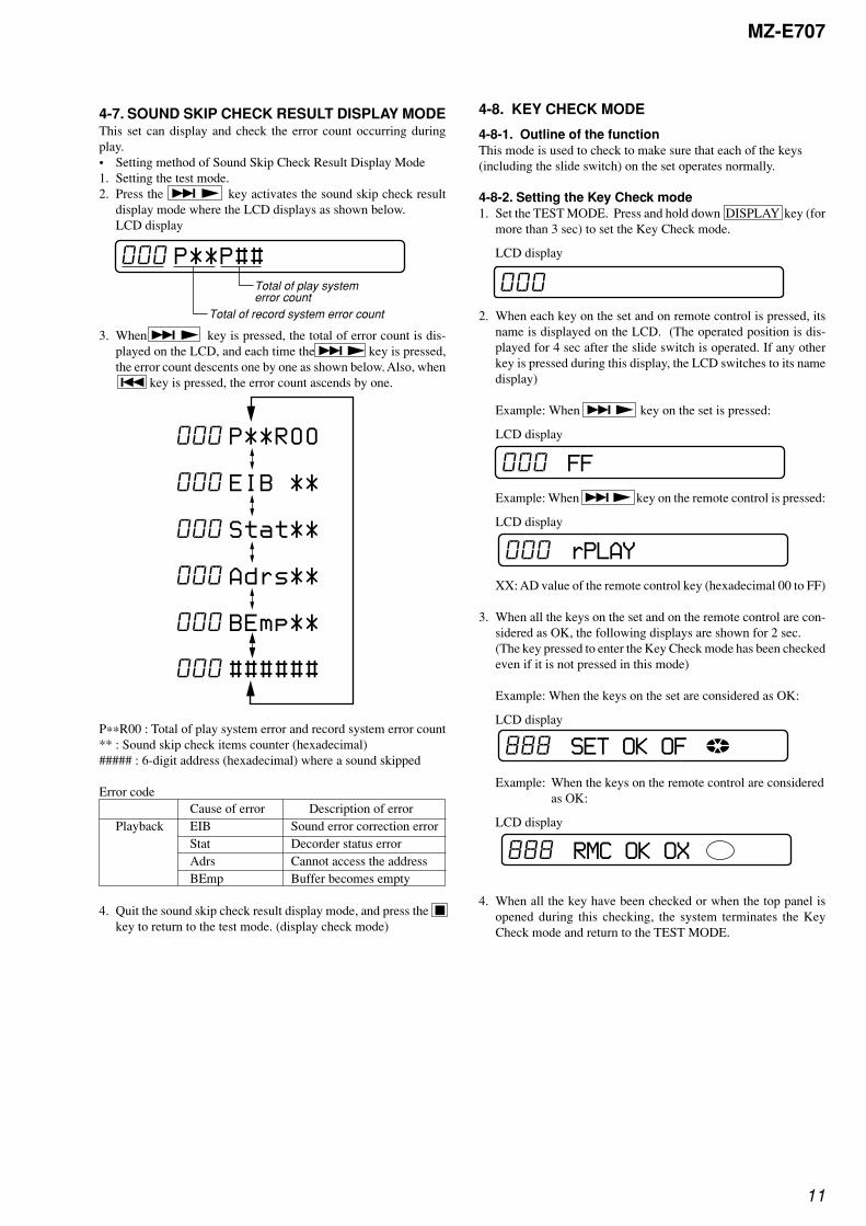
MAIN BOARD (SIDE A)
2 In the normal mode, operate the keys on the set and those on theremote control as specified below:Turn on HOLD switch on the set. Holding down x (STOP)key on the set, press the keys on the remote control in thefollowing sequence: > N t > N t . t . t > N
t . t > N t . t X t X
4-2-2. Operations when the TEST MODE is setWhen the TEST MODE is entered, the system switches to the dis-play check mode within the TEST MODE. From this mode, theother Test modes can be accessed.When the TEST MODE is set, the LCD repeats a cycle of the fol-lowing displays:
SECTION 4TEST MODE
888u
008 V1.000
F1SHUFF PGMSOUND 12
Test Mode(Display Check Mode)
Manual Mode
Servo Mode
Audio Mode
Power Mode
OP Alignment Mode
key
key
+
key+
key
x
x
>B
key
key
x key
. or
key
x key
Overall Adjustment Mode
Sound Skip Check Result Display Mode
Self-diagnostic Display Mode
Key Check Mode
DISPLAY key
DISPLAY key
(Press and hold down about 3 sec)
Terminate key checking or open the top panel.
C613
C605
C810
C802
C699
R607 R601 R80
C606
C610TP921
SHORT: TEST MODEOPEN: NORMAL MODE
TAP601
9
MZ-E707
2. During each test, press and hold down > N key or .key for a while to move the optical pickup on the sled outer orinner perimeter.
3. Each test item is assigned with a three-digit item number. The100th place is a major item, 10th place is a middle item, and unitplace is a minor item.
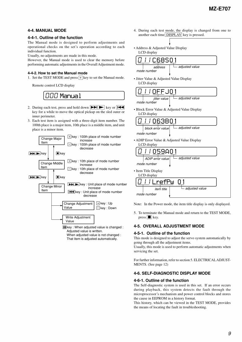
Note: In the Power mode, the item title display is only displayed.
5. To terminate the Manual mode and return to the TEST MODE,press x key.
4-5. OVERALL ADJUSTMENT MODE
4-5-1. Outline of the functionThis mode is designed to adjust the servo system automatically bygoing through all the adjustment items.Usually, this mode is used to perform automatic adjustments whenservicing the set.
For further information, refer to section 5. ELECTRICAL ADJUST-MENTS. (See page 12)
4-6. SELF-DIAGNOSTIC DISPLAY MODE
4-6-1. Outline of the functionThe Self-diagnostic system is used in this set. If an error occursduring playback, this system detects the fault through themicroprocessor’s mechanism and power control blocks and storesthe cause in EEPROM in a history format.This history, which can be viewed in the TEST MODE, providesthe means of locating the fault in troubleshooting.
4-4. MANUAL MODE
4-4-1. Outline of the functionThe Manual mode is designed to perform adjustments andoperational checks on the set’s operation according to eachindividual function.Usually, no adjustments are made in this mode.However, the Manual mode is used to clear the memory beforeperforming automatic adjustments in the Overall Adjustment mode.
4-4-2. How to set the Manual mode1. Set the TEST MODE and press + key to set the Manual mode.
Remote control LCD display
4. During each test mode, the display is changed from one toanother each time DISPLAY key is pressed.
• Address & Adjusted Value DisplayLCD display
• Jitter Value & Adjusted Value DisplayLCD display
• Block Error Value & Adjusted Value DisplayLCD display
• ADIP Error Value & Adjusted Value DisplayLCD display
• Item Title DisplayLCD display
000 Manual
Change Major Item
Change Middle Item
Change Minor Item
Change Adjustment Value
Write Adjustment Value
.
key : 100th place of mode number increase
+
key : 100th place of mode number decrease
key : 10th place of mode number increase
+
key : 10th place of mode number decrease
key : Up+
key : Down
key : When adjusted value is changed :Adjusted value is written.When adjusted value is not changed :That item is adjusted automatically.
keykey x
keyx
> N
key> N
key : Unit place of mode number increase
key : Unit place of mode number decrease
> N
X
011 C68S01address
mode numberadjusted value
011 OFFJ01jitter value
mode numberadjusted value
011 063B01block error value
mode number
adjusted value
011 059A01ADIP error value
mode number
adjusted value
011 LrefPw 01item title
mode number
adjusted value
10
MZ-E707
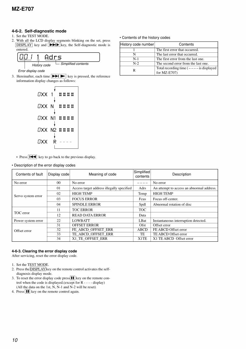
4-6-2. Self-diagnostic mode1. Set the TEST MODE.2. With all the LCD display segments blinking on the set, press
DISPLAY key and >B key, the Self-diagnostic mode isentered.
3. Hereinafter, each time > N key is pressed, the referenceinformation display changes as follows:
• Press . key to go back to the previous display.
• Contents of the history codes
History code number Contents1 The first error that occurred.N The last error that occurred.N-1 The first error from the last one.N-2 The second error from the last one.
RTotal recording time ( – – – – is displayedfor MZ-E707)
Contents of fault Display code Meaning of codeSimplified
Description contents
No error 00 No error – – – – No error
01 Access target address illegally specified Adrs An attempt to access an abnormal address.
Servo system error02 HIGH TEMP Temp HIGH TEMP
03 FOCUS ERROR Fcus Focus off-center.
04 SPINDLE ERROR Spdl Abnormal rotation of disc
11 TOC ERROR TOCTOC error
12 READ DATA ERROR Data
Power system error 22 LOWBATT LBat Instantaneous interruption detected.31 OFFSET ERROR Ofst Offset error
Offset error 32 FE_ABCD_OFFSET_ERR ABCD FE ABCD Offset error33 TE_ABCD_OFFSET_ERR TE TE ABCD Offset error34 X1_TE_OFFSET_ERR X1TE X1 TE ABCD Offset error
001 1 AdrsHistory code
Error display code
Simplified contents
0XX 1 # # # #
0XX N # # # #
0XX N1 # # # #
0XX N2 # # # #
0XX R – – – –
• Description of the error display codes
4-6-3. Clearing the error display codeAfter servicing, reset the error display code.
1. Set the TEST MODE.2. Press the DISPLAY key on the remote control activates the self-
diagnosis display mode.3. To reset the error display code press X key on the remote con-
trol when the code is displayed.(except for R - - - - display)(All the data on the 1st, N, N-1 and N-2 will be reset)
4. Press X key on the remote control again.
11
MZ-E707
4-8. KEY CHECK MODE
4-8-1. Outline of the functionThis mode is used to check to make sure that each of the keys(including the slide switch) on the set operates normally.
4-8-2. Setting the Key Check mode1. Set the TEST MODE. Press and hold down DISPLAY key (for
more than 3 sec) to set the Key Check mode.
LCD display
2. When each key on the set and on remote control is pressed, itsname is displayed on the LCD. (The operated position is dis-played for 4 sec after the slide switch is operated. If any otherkey is pressed during this display, the LCD switches to its namedisplay)
Example: When > N key on the set is pressed:
LCD display
Example: When > N key on the remote control is pressed:
LCD display
XX: AD value of the remote control key (hexadecimal 00 to FF)
3. When all the keys on the set and on the remote control are con-sidered as OK, the following displays are shown for 2 sec.(The key pressed to enter the Key Check mode has been checkedeven if it is not pressed in this mode)
Example: When the keys on the set are considered as OK:
LCD display
Example: When the keys on the remote control are consideredas OK:
LCD display
4. When all the key have been checked or when the top panel isopened during this checking, the system terminates the KeyCheck mode and return to the TEST MODE.
000
4-7. SOUND SKIP CHECK RESULT DISPLAY MODEThis set can display and check the error count occurring duringplay.• Setting method of Sound Skip Check Result Display Mode1. Setting the test mode.2. Press the > N key activates the sound skip check result
display mode where the LCD displays as shown below.LCD display
3. When > N key is pressed, the total of error count is dis-played on the LCD, and each time the > N key is pressed,the error count descents one by one as shown below. Also, when
. key is pressed, the error count ascends by one.
P**R00 : Total of play system error and record system error count** : Sound skip check items counter (hexadecimal)##### : 6-digit address (hexadecimal) where a sound skipped
Error codeCause of error Description of error
Playback EIB Sound error correction errorStat Decorder status errorAdrs Cannot access the addressBEmp Buffer becomes empty
4. Quit the sound skip check result display mode, and press the xkey to return to the test mode. (display check mode)
000 P**P##
Total of record system error count
Total of play system error count
000 P**R00
000 EIB **
000 Stat**
000 Adrs**
000 BEmp**
000 ######
000 FF
000 rPLAY
888 SET OK OF
888 RMC OK OX
12
MZ-E707
C910
R910
R964
R909
R903
C909C921
C908
C905
L905
L901
C907
10
14
15202528
2930 IC901
D903
TP901(VC)
digital voltmeter
TP901 (VC)
5-4. MANUAL POWER ADJUSTMENTS
5-4-1. Adjustment sequenceThe adjustments should be always performed in the following se-quence:
1 Vc PWM Duty (L) adjustment (item No.:762) r2 Vl PWM Duty adjustment (item No.:764) r3 Vd PWM Duty adjustment (item No.:765)
5-4-2. Vc PWM Duty (L) adjustment method1. Confirm that the power voltage is at 1.5 V DC.
2. Set the TEST MODE.
3. Set the overall adjustment mode and press PLAY MODE key,item No. will change to 762.
LCD display
SECTION 5ELECTRICAL ADJUSTMENTS
5-1. GENERALIn this set, CD and MO discs can be automatically adjusted by set-ting the Overall Adjustment mode within the TEST MODE,Before performing these automatic adjustments, it is necessary toclear the memory and adjust the power in the Manual mode.
5-2. NOTES FOR ADJUSTMENT
5-2-1. Jigs• CD disc TDYS-1 (part code: 4-963-646-01)• MO disc PTDM-1 (part code: J-2501-054-A)
or commercially available MO disc (recorded)• Digital voltmeter
5-2-2. Adjustment sequenceThe adjustments should be always performed in the followingsequence:
5-2-3. PowerThe power is supplied with 1.5 V DC from the battery case.
5-3. RESET NV
5-3-1. How to reset NV1. Set the TEST MODE.
2. Set the Manual mode and set the item No. 021, Reset NV.LCD display
1 Reset NV (Clear the memory)
2 Manual power adjustments
3 Electrical offset adjustments (Do not enter the disc)
4 Overall CD adjustments
5 Overall MO adjustments
6 RESUME clear
7 Rewrite the NV value
Overall adjustment mode
Manual mode
3. Press X key on the remote control.
LCD display
4. Press X key on the remote control again.
LCD display
5. Press x key to terminate the Manual mode and return to theTEST MODE.
021 Res NV CC
021 Res OK?
021 Res ***
021 Reset!
After reset is completed.
4. Connect a digital voltmeter to TP901 (VC) on the main boardand adjust + key (voltage up) and – key (voltage down) onthe remote control.
Adjustment value:2.35VStandard value:2.34 to 2.355V
MAIN BOARD (SIDE A)
762 VclPWM XX
5. Press X key to write the adjustment value.
13
MZ-E707
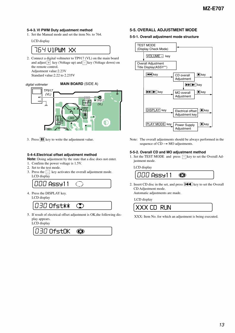
5-4-3. Vl PWM Duty adjustment method1. Set the Manual mode and set the item No. to 764.
LCD display
2. Connect a digital voltmeter to TP917 (VL) on the main boardand adjust + key (Voltage up) and – key (Voltage down) onthe remote control.Adjustment value:2.23VStandard value:2.22 to 2.235V
MAIN BOARD (SIDE A)
3. Press X key to write the adjustment value.
5-5. OVERALL ADJUSTMENT MODE
5-5-1. Overall adjustment mode structure
Note: The overall adjustments should be always performed in thesequence of CD t MO adjustments.
5-5-2. Overall CD and MO adjustment method1. Set the TEST MODE and press – key to set the Overall Ad-
justment mode.
LCD display
2. Insert CD disc in the set, and press . key to set the OverallCD Adjustment mode.Automatic adjustments are made.
LCD display
XXX: Item No. for which an adjustment is being executed.
764 VlPWM XX
000 Assy11
030 Ofst**
030 OfstOK
TEST MODE (Display Check Mode)
Overall AdjustmentTitle Display(ASSY**)
CD overall Adjustment
. key
VOLUME – key
keyx
MO overall Adjustment
> N key
> N key
keyx
Electrical offset Adjustment key
DISPLAY key keyx
keyxPower Supply Adjustment
PLAY MODE key
XXX CD RUN
000 Assy11
D901
D902
C903
C901 L902
TP917(VL)
digital voltmeter
TP917(VL)
5-4-4.Electrical offset adjustment methodNote: Doing adjustment by the state that a disc does not enter.1. Confirm the power voltage is 1.5V.2. Set to the test mode.3. Press the – key activates the overall adjustment mode.
LCD display
4. Press the DISPLAY key.LCD display
5. If result of electrical offset adjustment is OK,the following dis-play appears.LCD display
14
MZ-E707
3. If NG in the overall CD adjustments, return to Reset NV andperform from the electrical offset adjustment again.
LCD display
XXX: NG item No.
4. If OK through the overall CD adjustments, then perform overallMO adjustments.
LCD display
5. Insert MO disc in the set, and press > N key to set theOverall MO Adjustment mode. Automatic adjustments are made.
LCD display
XXX: Item No. for which an adjustment is being executed.
6. If NG in the overall MO adjustments, return to Reset NV andperform the adjustment again.
LCD display
XXX: NG item No.
7. If OK through the overall MO adjustments, press x key toreturn to the TEST MODE and terminate the Overall Adjust-ment mode.
LCD display
5-5-3.Resume clear method1. Setting the testmode.2. Set the Manual mode and set the item No.043(RESUME Clear).
LCD display
3. Press the X key.LCD display
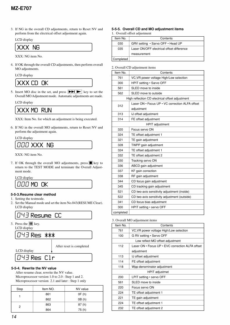
5-5-5. Overall CD and MO adjustment items1. Overall offset adjustment
Item No. Contents
030 GRV setting • Sarvo OFF • Head UP
035 Laser ON/OFF electrical offset difference
measurement
Completed
2. Overall CD adjustment items
Item No. Contents
761 VC,VR power voltage High/Low selection
300 HPIT setting • Sarvo OFF
561 SLED move to inside
562 SLED move to outside
High reflection CD electrical offset adjustment
312Laser ON • Focus UP • VC correction ALFA offset
adjustment
313 IJ offset adjustment
314 FE offset adjustment
HPIT adjustment
320 Focus servo ON
324 TE offset adjustment 1
321 TE gain adjustment
328 TWPP gain adjustment
324 TE offset adjustment 1
332 TE offset adjustment 2
330 Tracking servo ON
336 ABCD gain adjustment
337 KF gain correction
338 RF gain adjustment
344 CD focus gain adjustment
345 CD tracking gain adjustment
521 CD two-axis sensitivity adjustment (inside)
522 CD two-axis sensitivity adjustment (outside)
341 CD focus bias adjustment
300 HPIT setting • servo OFF
completed
XXX NG
XXX CD OK
XXX MO RUN
000 MO OK
000 XXX NG
043 Resume CC
043 Res ***
043 Res Clr
After reset is completedLCD display
3. Overall MO adjustment items
Item No. Contents
761 VC,VR power voltage High/Low selection
100 G RV setting • Servo OFF
Low reflect MO offset adjustment
112 Laser ON • Focus UP • EVC correction ALFA offset
adjustment
113 IJ offset adjustment
114 FE offset adjustment
118 Wpp denominator adjustment
HPIT adjustmet
200 LPIT setting • servo OFF
561 SLED move to inside
220 Focus servo ON
224 TE offset adjustment 1
221 TE gain adjustment
224 TE offset adjustment 1
232 TE offset adjustment 2
5-5-4. Rewrite the NV valueAfter resume clear, rewrite the NV value.Microprocessor version 1.0 to 2.0 : Step 1 and 2.Microprocessor version 2.1 and later : Step 1 only
Step Item NO. NV value
1861 0F (h)
862 0B (h)
2863 87 (h)
864 75 (h)
15
MZ-E707
Item No. Contents
230 Tracking servo ON
236 ABCD gain adjustment
237 KF gain adjustment
238 RF gain adjustment
244 FCS gain adjustment
245 TRK gain adjustment
READ GRV adjustment 1
100 R GRV setting • Servo OFF
562 SLED move to outside
120 Focus servo OFF
122 TON offset adjustment
121 TE gain adjustment
122 TON offset adjustment
123 TEIN offset adjustment
124 TWPP offset adjustment
130 Tracking servo ON
131 TWPP offset adjustment
136 ABCD gain adjustment
137 KF gain adjustment
139 ADIP BPF fo adjustment
144 FCS gain adjustment
145 TRK gain adjustment
134 TWPP gain adjustment
131 TWPP offset adjustment 1
132 TWPP offset adjustment 2
149 TWPP OP offset adjustment
138 RF gain adjustment
100 R GRV setting • Servo OFF
16
MZ-E707SECTION 6DIAGRAMS
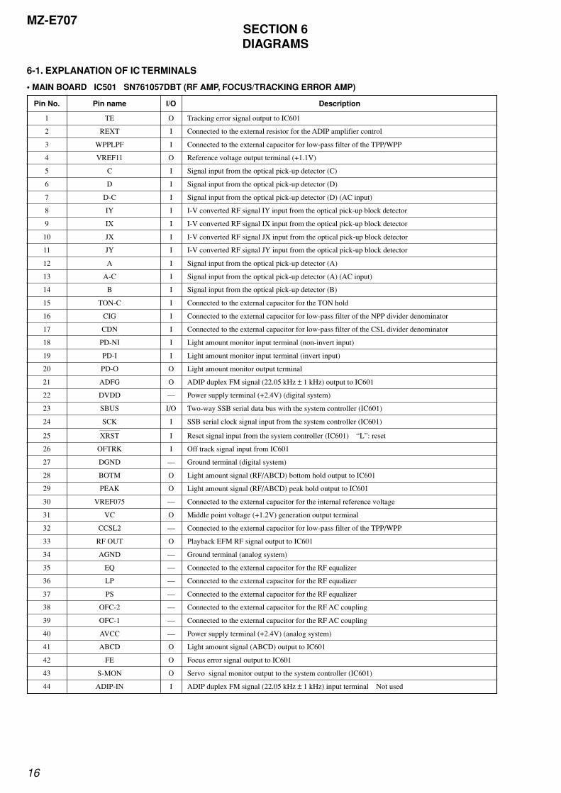
Pin No. Pin name I/O Description
1 TE O Tracking error signal output to IC601
2 REXT I Connected to the external resistor for the ADIP amplifier control
3 WPPLPF I Connected to the external capacitor for low-pass filter of the TPP/WPP
4 VREF11 O Reference voltage output terminal (+1.1V)
5 C I Signal input from the optical pick-up detector (C)
6 D I Signal input from the optical pick-up detector (D)
7 D-C I Signal input from the optical pick-up detector (D) (AC input)
8 IY I I-V converted RF signal IY input from the optical pick-up block detector
9 IX I I-V converted RF signal IX input from the optical pick-up block detector
10 JX I I-V converted RF signal JX input from the optical pick-up block detector
11 JY I I-V converted RF signal JY input from the optical pick-up block detector
12 A I Signal input from the optical pick-up detector (A)
13 A-C I Signal input from the optical pick-up detector (A) (AC input)
14 B I Signal input from the optical pick-up detector (B)
15 TON-C I Connected to the external capacitor for the TON hold
16 CIG I Connected to the external capacitor for low-pass filter of the NPP divider denominator
17 CDN I Connected to the external capacitor for low-pass filter of the CSL divider denominator
18 PD-NI I Light amount monitor input terminal (non-invert input)
19 PD-I I Light amount monitor input terminal (invert input)
20 PD-O O Light amount monitor output terminal
21 ADFG O ADIP duplex FM signal (22.05 kHz ± 1 kHz) output to IC601
22 DVDD — Power supply terminal (+2.4V) (digital system)
23 SBUS I/O Two-way SSB serial data bus with the system controller (IC601)
24 SCK I SSB serial clock signal input from the system controller (IC601)–––––––––––
25 XRST I Reset signal input from the system controller (IC601) “L”: reset
26 OFTRK I Off track signal input from IC601
27 DGND — Ground terminal (digital system)
28 BOTM O Light amount signal (RF/ABCD) bottom hold output to IC601
29 PEAK O Light amount signal (RF/ABCD) peak hold output to IC601
30 VREF075 — Connected to the external capacitor for the internal reference voltage
31 VC O Middle point voltage (+1.2V) generation output terminal
32 CCSL2 — Connected to the external capacitor for low-pass filter of the TPP/WPP
33 RF OUT O Playback EFM RF signal output to IC601
34 AGND — Ground terminal (analog system)
35 EQ — Connected to the external capacitor for the RF equalizer
36 LP — Connected to the external capacitor for the RF equalizer
37 PS — Connected to the external capacitor for the RF equalizer
38 OFC-2 — Connected to the external capacitor for the RF AC coupling
39 OFC-1 — Connected to the external capacitor for the RF AC coupling
40 AVCC — Power supply terminal (+2.4V) (analog system)
41 ABCD O Light amount signal (ABCD) output to IC601
42 FE O Focus error signal output to IC601
43 S-MON O Servo signal monitor output to the system controller (IC601)
44 ADIP-IN I ADIP duplex FM signal (22.05 kHz ± 1 kHz) input terminal Not used
6-1. EXPLANATION OF IC TERMINALS
• MAIN BOARD IC501 SN761057DBT (RF AMP, FOCUS/TRACKING ERROR AMP)
MZ-E707
17 17
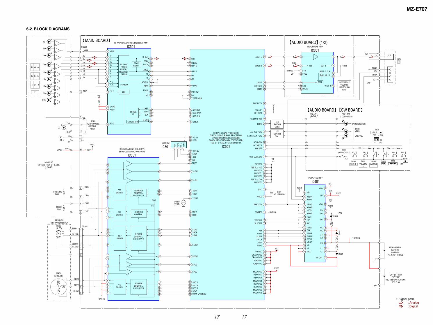
6-2. BLOCK DIAGRAMS
• Signal path.F : AnalogJ : Digital
12
160161
9
202
194195
221 XRF RST
PDS1
XCS NV
SI0
SCK0S00
XTEST
PD S0
S MON
SSB CLK
SSB DATA
VREF MON
MUTEXHP STB
BEEP
142RMC DTCK
13SET KEY 117WK DET
227HOLD SW
20RMC KEY
VC PWM164165
VL PWM
86FS4
235SLEEP236FFCLR8XRST21AVDD
52
CLKINM2
INM1
RF2
RF1
VRMCXWK3VSTB
XWK1XWK4
VD
XRST
10
44
VLD
19VG
18LG
9VL11VL
1612
L2L2
50VB
28L1
32L1
33VC OUT
7
2627
22
23
56
46
XWK23
SLEEP55FFCLR54
46VC36VC34VC245
21
120
13
4
2423
BEEP
STBMUTE
BEEP OUT A
BEEP OUT B
OUT BRCH
RCHIN B
+B
VCC
VREF IN
UNREG
VIF
REFERENCEVOLTAGE
SWITCHINGQ301
LEDSWITCH
Q803
LEDSWITCH
Q801
22 2
iJ301
RCHLCH
KEYRGND
DATA
VC
OFF ON
S808
D801,802(3 COLOR LED)
HOLD
S805VOLUME
+
S806GROUP
S804VOLUME
-
S809(OPEN/CLOSE)
VL
DVDD
35VCO
VC
42VIF
VIF
41VA
AVDD
DVDD
VG
UNREG
UNREG
234VLON VLON1
HEADPHONE AMP
IC301
POWER SUPPLY
IC901
-
89
8788
SPD U
SPD V
SPVS220 XRST MTR DRV
171815
S803.
S801xS802
>N
D901
D902
D903
DRY BATTERYSIZE "AA"
(IEC DESIGNATION LR6)1PC, 1.5V
VB MON
REC KEYSET KEY2
TSB MST VDD
10
19HALF LOCK SW
DIGITAL SIGNAL PROCESSOR,DIGITAL SERVO SIGNAL PROCESSOR,
EFM/ACIRC ENCODER/DECODER,SHOCK PROOF MEMORY CONTROLLER,
16M BIT D-RAM, SYSTEM CONTROL
IC601
TAP601(TEST)
141
LED O 211
LED RED PWM 167
LED GREEN PWM 163
1814
VC
AUDIO BOARD (1/2)
AUDIO BOARD (2/2)
SW BOARD
183
218240
MAIN BOARD
37
4445
46
47
56
74
7849
29
30
738491113153222
23119139151231
659
33
2928
41
42
14421
31
43
2423
4
89
1011121456
137
18 19
LASERAUTO POWER
CONTROLQ501
3
4
2
1911
20
13
12
5
18
9101415161778
6
1
TRACKINGCOIL
FOCUSCOIL
20
Jx Jy Jx
Ix Iy
Iy
Ix
Jx
Jy
A
B
C
D
PD
Ix
a
F
b c d
MINIDISCOPTICAL PICK-UP BLOCK
(LCX-4E)
LD
AVCC
S0S1
AVCC
S0
LD-K
LD-A
MON
DC
BAJyJxIxIy
D
D-C
PD-I
PD-O
C
BA
VREFVREF
A-C
JyJxIxIy
S1
RF AMP,FOCUSERROR,
TRACKINGERROR
TPP/WPP
APC
SERIALI/F
AVCC
2240
DVDDAVCC
VIF
RF OUT
PEAK
BOTM
ABCD
FE
ADIP IN
TE
ADIP
PD-NI
VC
AOUT L
AOUT R
VDIOSCDRAMVDD0
DSPVDD0DSPVDD1
MCUVDD1DSPVDD2DSPVDD3MCUVDD2MCUVDD3
DRAMVDD1JTAGVDD
FLASHVDD
MCUVDD0
SBUSSCK
S MON
XRST
PEAK/BOTM
RFI
PEAKBOTM
ABCD
FE
TE
VC
ADFG
APCREF
VC
DVDD
RF AMP,FOCUS/TRACKING ERROR AMP
IC501CN501
TRK+
TRK-
FCS+
FCS-
30
95
94
93
102
99
979698
8382
101
196176
100
76143154
210241
24
25
2623
33 2827
8180
47
14 1516
424344
3435
37
89654
UNREG
52
41
HI-BRIDGECONTROL/
PRE DRIVER
HI-BRIDGECONTROL
PREDRIVER
3 PHASECONTROL/
PRE DRIVER
3 PHASECONTROL/
PRE DRIVER
PREDRIVER
PREDRIVER
PREDRIVER
2446
2545
53
54
1
565548
FOCUS/TRACKING COIL DRIVE,SPINDLE/SLED MOTOR DRIVE
IC551
SLCU
DIFVDD0
VIF
TSB SLV VDDMIFVDD0MIFVDD1MIFVDD2
TSB SLV CHKMIFVDD3
SLCV
OSCITFDR
OSCOTRDR
FRDR
SLDVSRDRSFDR
SLDW
SLCW
SPCU
SPCV
SPCW
FFDR
X60145.1584MHz
SLED1+
SLED1-
SLED2+SLED2-
CLVU
CLVV
CLVW
MINIDISCMECHANISM BLOCK
M902(SLED)
M901(SPINDLE)
4
2
31
8
7
6
5
CN551
32
13
39
1720
19
18
90 SPD W2
BIAS
OE
11
S-MONITOR
25
RECHAGEABLEBATTERYNH-14WM
1PC, 1.2V 1400mAh
219
EEPROM
IC801 4DI
3DO
2SK
1XC
S
181180179
D802 (ORANGE)
D801 (RED)
(GREEN)
MZ-E707
18 18
2 3 4 5 6 7 8 9
A
1
B
C
D
E
F
C505
C519
C530
C503
R503 R5
19
C854
C853
C603
C526
C613
C605
C810
C802
C616
C607
C699
C612
C611
C515
C513
C511
C510
C508
C910
R910
R807
R827
R615
R603 R606 R605 R614 R612
R607 R601 R602R804
R501
R521
R516
R505
R921
R946
R948
R920
R964
R950
R954
C920
R909
R903
R818
R817
C851
R819
R806
R515
R808
R613
R609
R526
R517
R525 R9
63
C807
C559
C558C557
C601C806
C615
C509
C516
C504
C501
C502
C918
C917 C915
C909C921
C908
C905
Q501
BCE
D901
D902
C903
C901
L503L904
L905
L901
L902
MAIN BOARD (SIDE A)
C606
C610
C524
C922
C904
C919
C911
C925
C907
1
5
10
14
15202528
43
2930
35
40
45 50 555642
IC901
1
5
10
14
15 20 25 28
43
2930
35
40
45505556
42
IC551
IC501
1
1
5
5
10
10
15
15
20
20
22
444035302523
CN501
OPTICAL PICK-UPBLOCKLCX-4E
X601
*IC601
TP921
TP604
TP605
TP565
TP560
TP602TP601
TP533
TP603
SHORT: TEST MODEOPEN: NORMAL MODE
TAP601
FB801
FB802
IC8011
1 5 15
2 10
19
20
4
8
5
RB55
3
RB554
D855
32
1
45
CN801
A AUDIO BOARDCN802
D201
D903
D101
M
M902SLED MOTOR
M901SPINDLE MOTOR
123
456
78
J3012
1
5
8
CN551
11(11)1-682-471-
C618
DRY BATTERYSIZE "AA"
(IEC DESIGNATION LR6)1PC, 1.5V
MOTOR FLEXIBLE BOARD
RECHAGEABLEBATTERYNH-14WM
1PC, 1.2V 1400mAh
TP903(VD)
TP917(VL)
TP901(VC)
C563
C564
C565
C527
R839
R832 R831
R833 R830
R834
R835
R962
R960
R961
C604
C999
C952
Q801
C529 BCE Q803
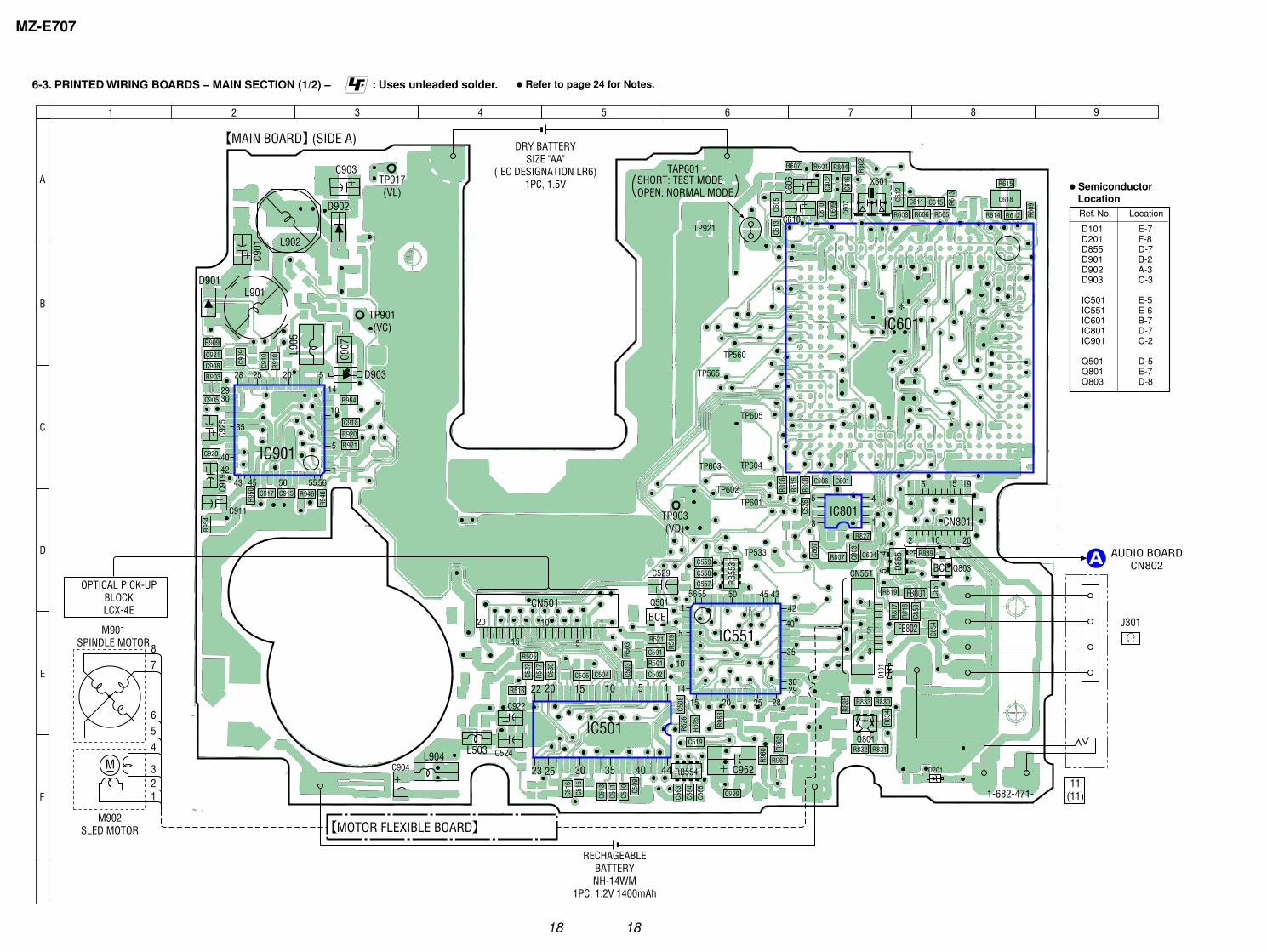
D101 E-7 D201 F-8 D855 D-7 D901 B-2 D902 A-3 D903 C-3
IC501 E-5 IC551 E-6 IC601 B-7 IC801 D-7 IC901 C-2
Q501 D-5 Q801 E-7 Q803 D-8
6-3. PRINTED WIRING BOARDS – MAIN SECTION (1/2) – z Refer to page 24 for Notes.
Ref. No. Location
z Semiconductor Location
: Uses unleaded solder.
MZ-E707
19 19
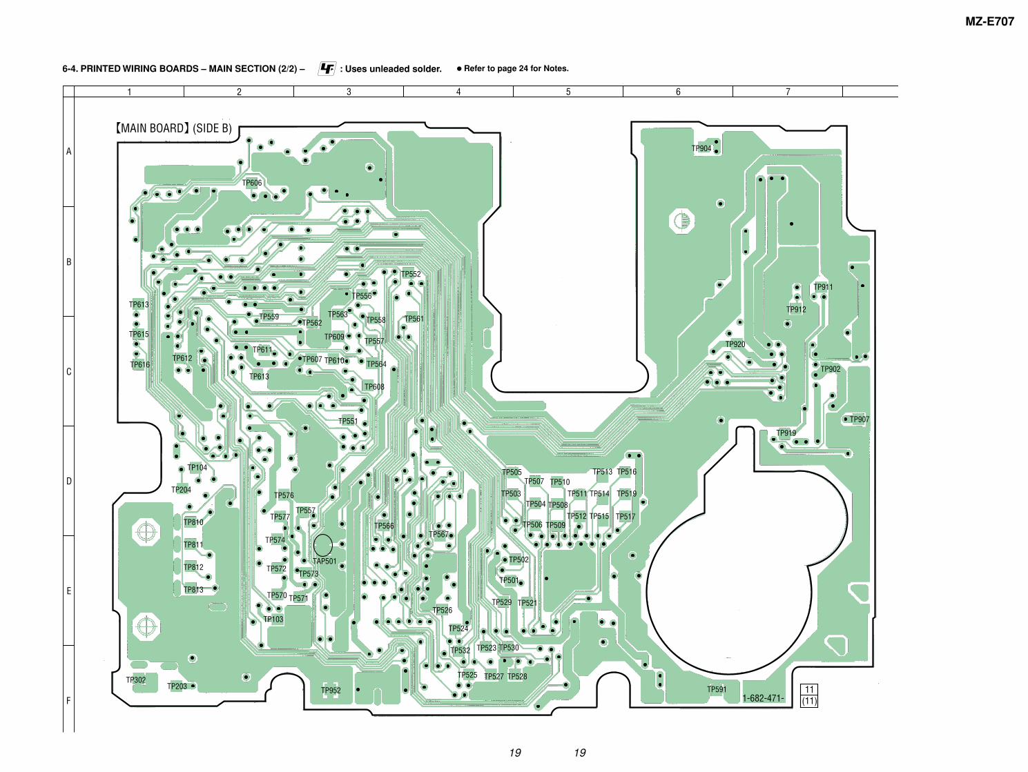
6-4. PRINTED WIRING BOARDS – MAIN SECTION (2/2) – z Refer to page 24 for Notes. : Uses unleaded solder.
2 3 4 5 6 7
A
1
B
C
D
E
F
MAIN BOARD (SIDE B)
11(11)1-682-471-
TP611TP612
TP613
TP615
TP616TP613
TP559TP562
TP563
TP609
TP610TP607
TP558
TP606
TP552
TP556
TP561
TP564
TP608
TP557
TP551
TP104
TP204
TP810
TP811
TP812
TP813
TP302TP203
TP103
TP570
TP572TP573
TP571TP526
TP952
TP525
TP532
TP524
TP530TP523
TP527 TP528
TP529 TP521
TP501
TP502
TP591
TP516
TP919
TP907
TP902
TP920
TP912
TP911
TP904
TP519
TP517
TP513
TP514
TP515
TP510TP511
TP512
TP507
TP508
TP509TP577
TP576
TP557
TAP501
TP574TP567
TP566
TP503
TP505
TP504
TP506
MZ-E707
20 20
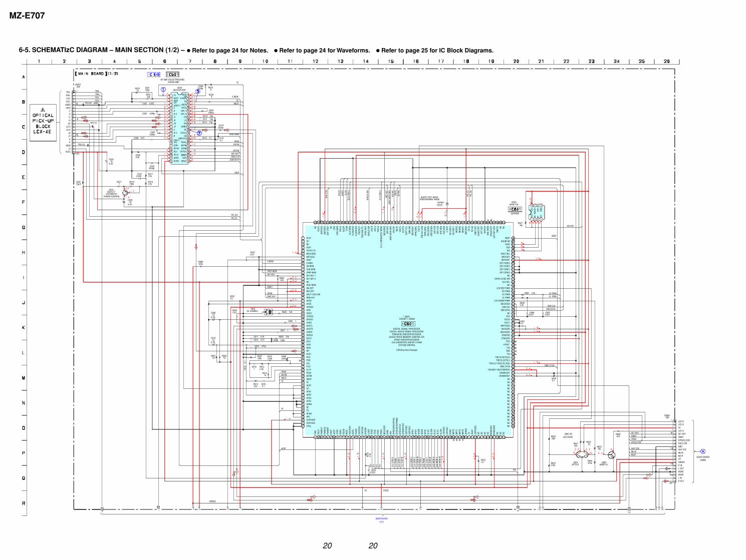
6-5. SCHEMATIzC DIAGRAM – MAIN SECTION (1/2) – z Refer to page 24 for Notes. z Refer to page 24 for Waveforms. z Refer to page 25 for IC Block Diagrams.
C505
C502TP5105
C503
TP5118
TP5112
C508 R525IC501
R526
C511C510
C516
C501
R501
C509
Q501
C529
R521 R519
C527 R517
R516
C530
R505
C802
C611
C607
C612R605
R606
C613
C610
C616
R613
C603
C604
C601
R808
C806 C807
CN501
R806
R603X601
TAP601
R827
CN801
L50310µH
C526
C524
R503
C513
R804
C605
R607 R615
C519
C504
C515
R614
C615
R612
R601
IC801
R609
C618
R602
C606
R807
R831R833
Q801 Q803
R839
C810
R830
R834
R832
R835
R515
IC601
C699
0.01
0.033(GND)
3300p
1500p 0SN761057DBT
0
10p10p
0.1
100p
33k
3300p
2SA1577
106.3V
1 100k
0.033 2.2k
2.2k
2200p
2.2k
0.1
0.01
1
0.4710k
100k
470p
106.3V
0.1
220
0.1
0.1
0.1
3.3k
0.047 0.047
20P
100k
15045.1584MHz
1M
20P
0.033
106.3V
1k
10p
47k
1
100k 3.3M
3300p
3300p
0.1
1k
0.1
3.3k
10
AK6417AL
220k
1
10
106.3V
3.3k
33015k
XP1510 UN9214J
470
0.01
68k
470k
33
470k
2.2k
CXD2671- 206GA
0.01
12
1716141398765412
151811
TRK-TRK+FCS-FCS+
VREF MON
ADIP
PEAKBOTM
FEABCD
TE
CLV
MON
WCL
V M
ON V
CLV
MON
U
CLV
CON
WCL
V CO
N V
CLV
CON
UCL
V PW
M
TR1
TF1
SLD
PWM
FF1
FR1
ADIP
PEAKBOTM
FEABCD
TE
RMC DTCKXH
OLD
SW
SET KEYXWK1OPENXHOLD SW
BEEPMUTEXHP STB
BEEP
MUT
E
XHP
STB
VREF MON
S MON
PD_S
0PD
_S1
SSB CLKSSB DATA
OFTR
K
XRF
RST
XRST
MTR
DRV
XCS
NY
XCS NY
CLV
CON
U
VC PWNVL PWN
VLON
SLEE
PFF
CLR
SET KEY
XWK1
OPENRMC KEY
FS4
PD_S0PD_S1
S MON
OFTRKXRF RSTSSB CLK
SSB DATA
SLD
CON
VSL
D CO
N W
SLD
CON
U
SLD
MON
USL
D M
ON V
SLD
MON
W
SLD
CON
U
TEREXTWPP
CDD-CIYIXJXJYAA-CB
TON-CCIGCDNPD-NIPD-IPD-O
DVDD
ADIP-IN
S-MONFE
ABCDAVCCOFC-1OFC-2
PSLPEQ
AGND
CCSL2VC
VREF075
PEAKBOTMDGND
OFTRK
SCKSBUS
AUTOMATICPOWER CONTROL
ADFGXRST
RF
LPFVREF11
RF AMP,FOCUS/TRACKINGERROR AMP
TRK-TRK+FCS-FCS+
AGNDVREF
CDIYIX
LD-ALD-K
JXJYAB
MON
AVCC
SO
SI
VCC
EEPROM XBUS
YRS
TGN
D
XCS
SK DI DO
DIGITAL SIGNAL PROCESSOR,DIGITAL SERVO SIGNAL PROCESSOR,
EFM/ACIRC ENCODER/DECODER,SHOCK PROOF MEMORY CONTROLLER,
ATRAC ENCODER/DECODER,
CSP(Chip Size Package)
D/A CONVERTER,16M BIT D-RAMSYSTEM CONTROL
MCUVDD0MIFVSS3XRSTS MONVB MONCHG MON
SET KEY 1SET KEY 2
HIDC MONWK DETREC KEY
AVDDAVSSVDIOSCOSCIOSCO
HALF LOCK SWRMC KEY
VSIOSCDAVDDVREFLAOUTLAOUTRVREFRDAVSSASYOASYIAVDIBIASRFIAVS1PCOPDOFILIFILOCLTVPEAKBOTMABCDFEAUX1VCADIOADRTAVD2AVS2ADRBSETEDCHGAPCDSPVDD0DSPVSS0XTSL
BEEPXGUM ON
SO0SI0
AOUT SELMIFVSS1MIFVDD1
SET CODE3SET CODE2SET CODE1SET CODE0
OPEN CLOSE SWCLK SEL
NC
VC PWMVL PWM
MCUVSS0
EVATEST0TEST1
MIFFVSS0MIFVDD0
MCUVDD2
SSB CLKSSB DATA
JTAGVSSJTAGVDD
TDO
TCKTMSTDI
TSB SLV0(TSL0)TSB SLVI(TSLI)
TSB SLV VDD(TSLVDD)RMC DTCK
TSB MST VDD(TSMVDD)DRAMVSS1DRAMVDD1
NCNCNCNCNCNCNCNCNCNCNCNCNCNCNCNC
NCTE
ST2
MIF
VSS2
MIF
VDD3
XHP
STBY
CHG
CHG
GAIN
FFCL
RSL
EEP
VLON
SLD
MON
FLAS
HVSS
FLAS
HVDD
PROT
ECT
SYNC
REC
XAVL
SCL
V U
MON
(SPD
L M
ON)
MCU
VDD3
XRF
RST
XRST
MTR
DRV
XCS
NYM
UTE
CS R
TCXO
PT C
TL
MCU
VSS1
TSB
SLV
CHK
LCD
STB
XCS
LCD
XPD
ADA
XCS
ADA
HD C
ON 2
HD C
ON 1
MOD
E1M
ODE2
MOD
E3
MIF
VDD2
PD S
IPD
SO
XMIC
DET
XJAC
K DE
TOP
T DE
TXP
ATCH
LCD
RST
AUX
XMUT
E
NC
DIN1
DOUT
PWM
LPPW
MLN
ADDT
LRCK
XBCK
MVC
I
PWM
RP
DSPV
DD1
ADFG
FOCN
TDI
FVDD
0DI
FVSS
0AP
CREF
LDDR
TRDR
TFDR
FFDR
FRDR
MCU
VDD1
FGIN
FS4
SPFD
/SPV
S/PW
M3
SPCU
SPCV
SPCW
SPDV
/RTG
1SP
DW/R
TG2
DSPV
DD2
DSPV
SS1
SLDV
SLDW
SLCU
SLCV
SLCW
DIFV
DD1
DIFV
SS1
EFM
O
MNT
3M
NT2
MNT
1M
NT0
SENS
ETX RE
CPDS
PVDD
3NC
DRAM
VDD0
NC NC NC NC NC NC SET KEYXWK1
HOLD SWGNDXHP STBMUTEBEEPVIFUNREGR INL OUTAGNDAGNDL INR OUT
AUDIO BOARDCN802
SHORT:TEST MODEOPEN:NORMAL MODE
(TEST)
VREF MON
SPRD
/SPD
U/RT
G0
DRAM
VSS0
XTRST
SCK0
XHOL
D SW
*
MAIN BOARD(2/2)
NC
PAUS
E KE
YM
IC S
ENS
X TE
ST
ORPL
EDGH
RECL
EDGH
ORPL
EDGL
LED
OOP
RLED
RL
GND
SW
VGCT
L
JOG
AJO
G B
TSB
SSB
CTL
NC
SCS1SI1NCSCK178 DD CTL
NC
DADT
FS25
6
SRDR
SFDR
NC
LED RED PWMVD PWM
LED GREEN PWM
NC
LED GLED R
VCLED O
OPEN/CLOSE
DVDDVC
UNREG
LED DRIVEQ801,83
MZ-E707
21 21
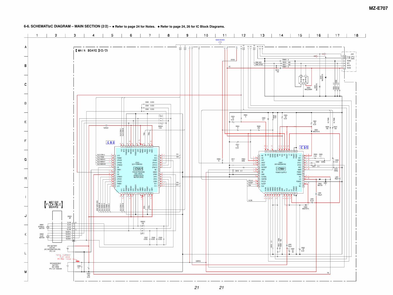
6-6. SCHEMATIzC DIAGRAM – MAIN SECTION (2/2) – z Refer to page 24 for Notes. z Refer to page 24, 26 for IC Block Diagrams.
CN551
C557 C558 C559
D855
R817R818
D201
D101
C851
R819
L901
D901
C901
C917
C918 R9
20R9
21
C903C904
L90410µH
L90247µH
D902
R903 C905
C921
C909
D903 C907
C910
R909 R910
FB801
FB802
RB553
C915
J301
C999
IC901
R964R950
C925
IC551
C565
C564
C563
TAP501RB554
C920
C908
C854
C853
C919R963
R948
R954 R946
C911
C952
L905100µH
68µH
8P
0.033 0.033 0.033
MAZZ068H
100100
NAZS
0270
NAZS
0270
0.1
1M
MA2YD15
226.3V
0.1
0.1 10
k15
0k
476.3V22
4V
MA2YD15
2.2k 0.1
0.1
0.01
MA729 1
1000p
10k 10k
0
0
10k
0.1
0.1
XPC18A32AFCR2
680k1k
226.3V
SC111258FCR2
0.033
0.033
0.033
3.3k
0.1
3300p
0.1
0.00
68
106.3V
0
150k
0 22k
106.3V
1006.3V
1 2 12 154 5 6 7 8 9 11 13 14 16 17 18
CLV
MON
WCL
V M
ON V
CLV
MON
U
CLV
CON
WCL
V CO
N V
CLV
CON
UCL
V PW
M
XRST
MTR
DRV
FFCLRSLEEPFS4
VLON
RMC DTCKRMC KEY
VC P
WN
VL P
WN
SLD MON WSLD MON VSLD MON U
SLD CON USLD PWM
SLD
CON
VSL
D CO
N W
TR1TF1
FF1FR1
FCS-
FCS+
TRK-
TRK+
FOCUS/TRACKINGCOIL DRIVE,
SPINDLE/SLEDMOTOR DRIVE
VLON
XWK1
VSTB
GND
VL VLO
VL L2 PGND
2PG
ND2
XWK2
XWK3
XWK4
VRM
C
VAVA
FBVD
FBVI
FFB
GND VC VCO VC L1 NC
PGND
1PG
ND1
VCOU
T
DTC1DTC2
RF2INM2
PWM1PWM2
VGLG
PGND2L2
NC
L1RF1
INM1
NCVDVC2XRSTCRSTRSTREFVREFVBGNDCLKSELVAIFONFFCLRSLEEPCLK
GND2CPWICPVICPUICOM
F11R11
F12R12
CLVNCLVUCLVV
CLVWSLED1+SLED2+SLED1-SLED2-
SLEDMOTOR
MOTORSPINDLE
M901
M902
POWER SUPPLY
VIF
RVDDDATAKEYRGND
DRY BATTERYSIZE"AA"
BATTERYNH-14WM
RECHARGEABLE
(IEC DESIGNATION LR6)1PC.1.5V
1PC.1.2V 1400mAh
MAIN BOARD(1/2)
VC
DVDD
UNREG
VG
U12PWM2CPUO2CPVO2
OEGND1VCVGCPWO1CPVO1CPUO1PWM1U11
CPWO2
COM2CPU12CPV12CPW12
NC
V12
W12
PGND
W2
WO2
VMVW
2VO
2PG
NDUV
2UO
2VM
U2VM
R2RO
2PG
ND2
FO2
VMF2
V11
W11
PGND
W1
WO1
VMVW
1VO
1PG
NDUV
1U0
1VM
U1VM
R1RO
1PG
ND1
FO1
VMF1
MZ-E707
22 22
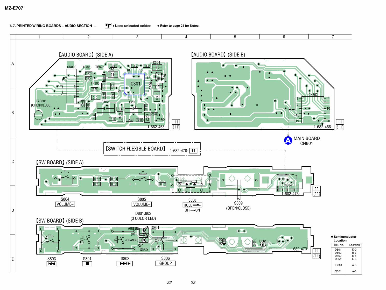
6-7. PRINTED WIRING BOARDS – AUDIO SECTION – z Refer to page 24 for Notes. : Uses unleaded solder.
2 3 4 5 6 7
A
1
B
C
D
E
C204
R203 R204
R303 R302
R106
R104
R206
R103
R101
R102
R202
R201
R301
C303
C302
C104
C803
C804
C201
C101
Q301
BCE
AUDIO BOARD (SIDE B)AUDIO BOARD (SIDE A)
11(11)1-682-468-
11(11)1-682-468-
C301
C102 C202
C304
C306
C305
C103
C203
TAP801(OPEN/CLOSE)
TP826 TP825
TP305
TP304
1
5
15
2
10
19 20
CN802
A MAIN BOARDCN801
1 6
7
12
1318
19
IC30124
1
5
9
CN803
19 CN804
111-682-470-SWITCH FLEXIBLE BOARD
SW BOARD (SIDE B)
SW BOARD (SIDE A)
S808HOLDc
OFFtON
S809(OPEN/CLOSE)
R815
C860
R813
R814
R811
R812
11(11)1-682-473-
11(11)
1-682-473-
S804VOLUME–
S805VOLUME+
S806GROUP
S801x
S803.
S802>B
D801,802(3 COLOR LED)
D801
D802
(GREEN)
(RED)
(ORANGE)
D860 D861
D801 D-3 D802 E-3 D860 E-5 D861 E-6
IC301 A-3
Q301 A-3
Ref. No. Location
z Semiconductor Location
MZ-E707
23 23
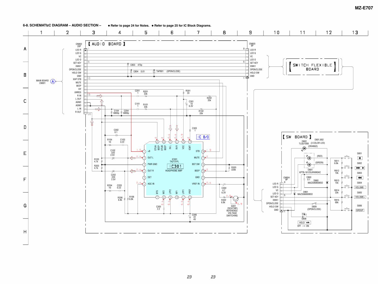
6-8. SCHEMATIzC DIAGRAM – AUDIO SECTION – z Refer to page 24 for Notes. z Refer to page 25 for IC Block Diagrams.
IC301
C204
C201 R201
R202
R104 C103
R106
R103
R203
R206
R204 C203
C101
R102
R101
C104
C305
C306
C304
R302
R303
C804 TAP801
CN802
S801
S802
S803
S804
S805
S808
S809
R811
R812
R813
R814
R301
C301
C303C302
Q301
C803
CN803
CN804
S806
R815
D802
D801
C102
C202
D861
D860C860
TA2131FL
6800p
1 33k
33k
10 0.22
6.8k
4.7k
4.7k
6.8k
10 0.22
1
33k
33k
6800p
2.2
224V
4.76.3V
6.8k
220k
0.01 (OPEN/CLOSE)
20P
(OPEN/CLOSE)
6.8k
10k
15k
33k
33
106.3V
10.1
2SC4738FL
470p
9P
9P
68k
TLQU1008
2202.5V
2202.5V
MAZS068008SO
MAZS068008SO0.1
SET KEYXWK1
OPEN/CLOSEHOLD SW
GNDXHP STB
MUTEBEEP
VIFUNREG
R INL OUTAGNDAGND
L INR OUT
STB
MUTE
BST SW
BEEP
GND
VREF IN
+B
OUT L
PWR GND
OUT R
DET
AGC IN
BTS
NF2
LPF2
NF1
LPF1
VREF
OTUA
BEEP IN L
IN R
VCC
ICM
T
BEEP
OTUB
HOLDONOFF
MAIN BOARDCN801
REFERENCEVOLTAGE
SWITCHING
LED RLED G
VCLED O
LED RLED G
SET KEYXWK1OPEN/CLOSEHOLD SWGND
VCLED O
LED RLED G
SET KEYXWK1
OPEN/CLOSEHOLD SW
GND
VCLED O
GROUP
KPTB-1612SURKMGKC
VOLUME-
VOLUME+
HEADPHONE AMP
1
5
9
1
5
9
(ORANGE)
(GREEN)
(RED)
D801,802(3 COLOR LED)
MZ-E707
24 24
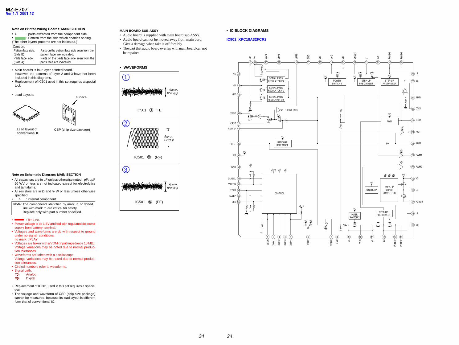
• IC BLOCK DIAGRAMS
IC901 XPC18A32FCR2
Note on Schematic Diagram: MAIN SECTION
• All capacitors are in µF unless otherwise noted. pF: µµF50 WV or less are not indicated except for electrolyticsand tantalums.
• All resistors are in Ω and 1/4 W or less unless otherwise
specified.• f : internal component.
Note: The components identified by mark 0 or dottedline with mark 0 are critical for safety.Replace only with part number specified.
• : B+ Line.• Power voltage is dc 1.5V and fed with regulated dc power
supply from battery terminal.• Voltages and waveforms are dc with respect to ground
under no-signal conditions.no mark : PLAY
• Voltages are taken with a VOM (Input impedance 10 MΩ).Voltage variations may be noted due to normal produc-tion tolerances.
• Waveforms are taken with a oscilloscope.Voltage variations may be noted due to normal produc-tion tolerances.
• Circled numbers refer to waveforms.• Signal path.
F : AnalogJ : Digital
• Replacement of IC601 used in this set requires a specialtool.
• The voltage and waveform of CSP (chip size package)cannot be measured, because its lead layout is differentform that of conventional IC.
Note on Printed Wiring Boards: MAIN SECTION
• X : parts extracted from the component side.• : Pattern from the side which enables seeing.(The other layers' patterns are not indicated.) Caution:
Pattern face side: Parts on the pattern face side seen from the(Side B) pattern face are indicated.Parts face side: Parts on the parts face side seen from the(Side A) parts face are indicated.
• Main boards is four-layer pritnted board.However, the patterns of layer 2 and 3 have not beenincluded in this diagrams.
• Replacement of IC601 used in this set requires a specialtool.
• Lead Layouts
Lead layout ofconventional IC
surface
CSP (chip size package)
56
55
42 41 40
VLON
XWK1
XWK2
XWK3
XWK4
VSTV
7
VRM
C
GND
8
VL VLO
9 10
VL
11
L2
12
PGND
2
13
PGND
2
VIF
VA VAFB
VDFB
VIFF
B
GND
VC VCO
VCOU
T
L1VC NC PGND
1
PGND
1
14
15
16
17
18
19
20
39 38 37 36 35 34 33 32 31 30 29
28
27
26
25
24
23
22
21
1 2 3 4 5 6
54
53
52
51
50
49
48
47
46
45
44
43 L1
RF1
INM1
DTC1
DTC2
RF2
INM2
PWM1
PWM2
VG
LG
PGND2
L2
NC
NC
VD
VC2
XRST
CRST
RSTREF
VREF
VB
GND
CLKSEL
VAIFON
FFCLR
SLEEP
CLK
SERIAL PASSREGULATOR VA
SERIAL PASSREGULATOR VD
SERIAL PASSREGULATOR VIF
BANDGAPREFERENCE
VC
XRST (INT)
VC
VC
VSTB VC VB
POWERSWITCH 1
VG
STEP-UPPRE DRIVEER
VG
STEP-UPPRE DRIVEER
PWM
VG
VC
VG
VG
VC
STEP-UPDC/DC
CONVERTORSTART-UP
VCVB
VB
VG VG
STEP-UPPRE DRIVEERPWER
SWITCH 2
VG
VC VB
VC
VSTB
CONTROL
VC
MAIN BOARD SUB ASSY• Audio board is supplied with main board sub ASSY.• Audio board can not be moved away from main bord. Give a damage when take it off forcibly.• The part that audio board overlap with main board can not
be repaired.
• WAVEFORMS
1
IC501 1 TE
2
3
IC501 ed (RF)
IC501 rs (FE)
Approx.12 mVp-p
Approx.1.2 Vp-p
Approx.10 mVp-p
Ver 1.1 2001.12
25
MZ-E707
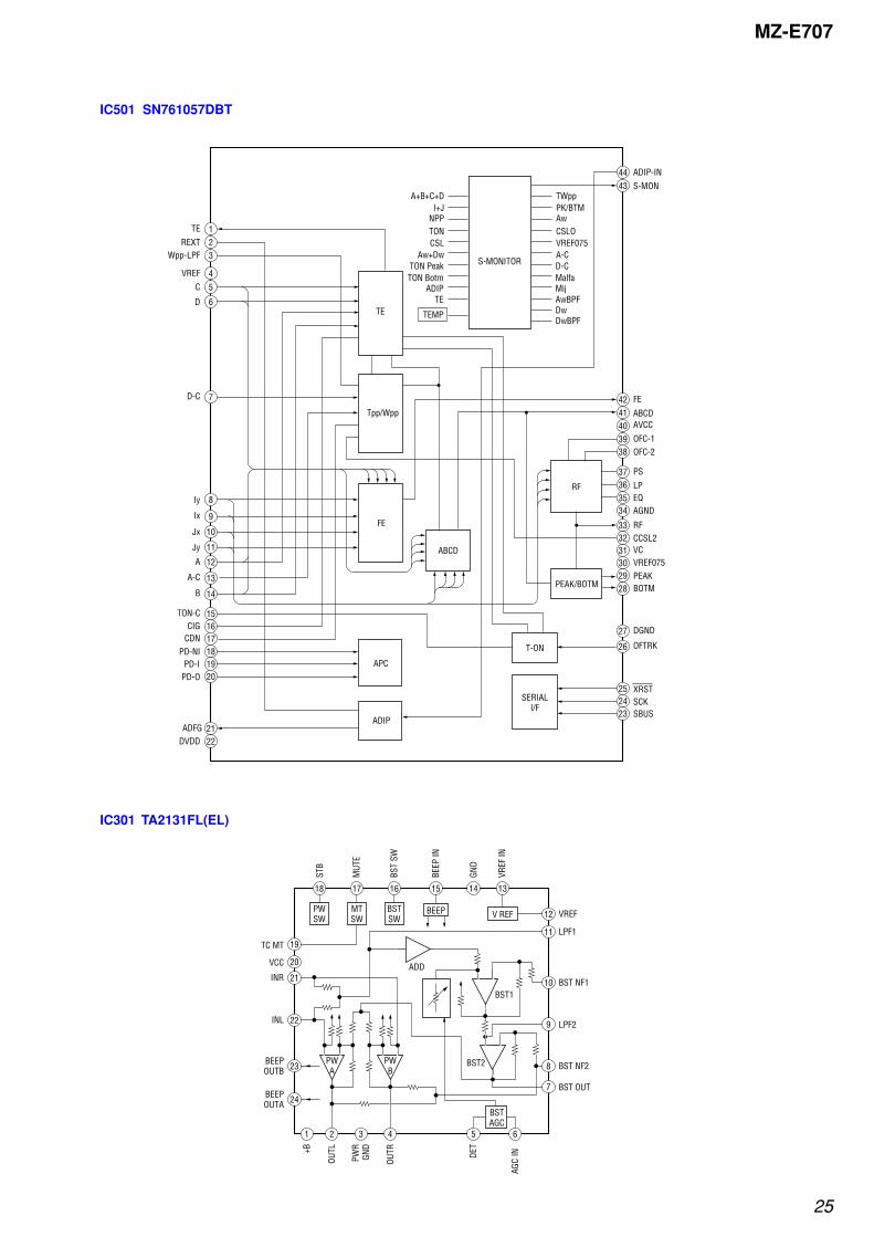
IC501 SN761057DBT
IC301 TA2131FL(EL)
1TE
REXTWpp-LPF
VREF
C
D
D-C
Iy
Ix
Jx
Jy
A
A-C
B
ADIP-IN
FE
ABCDAVCC
OFC-1OFC-2
PS
LPEQAGND
RFCCSL2VC
XRSTSCKSBUS
VREF075PEAKBOTM
DGND
OFTRK
S-MON
TON-CCIG
CDN
ADFGDVDD
PD-NIPD-I
PD-O
4344
TWppPK/BTMAwCSLOVREF075A-CD-CMalfaMijAwBPFDwDwBPF
42
38
37363534
31302928
27
26
252423
39
4140
23
4
5
6
7
8
9
10
11
12
13
14
151617181920
2122
A+B+C+DI+J
NPPTONCSL
Aw+DwTON PeakTON Botm
ADIPTE
TEMP
3332
S-MONITOR
TE
RF
FE
APC
ADIP
T-ON
SERIALI/F
PEAK/BOTM
ABCD
Tpp/Wpp
V REFMTSW
BSTSW
BEEP
19
20
21
22
23
24
18 17 16 15 14 13
PWSW 12
11
10
8
7
BST1
9
BST2
654321
BSTAGC
PWB
PWA
ADD
TC MT
VCC
INR
INL
BEEPOUTB
BEEPOUTA
+B
OUTL
PWR
GND
OUTR DE
T
AGC
IN
BST OUT
BST NF2
LPF2
BST NF1
LPF1
VREF
VREF
IN
GND
BEEP
IN
BST
SW
MUT
E
STB
26
MZ-E707
IC551 SC111258FCR2
14
13
56 55
CPW
I2
CPVI
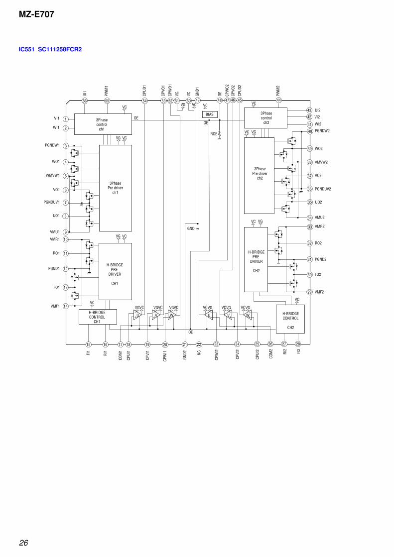
2
CPUI
2
COM
2
RI2
FI2
UI1
PWM
1
CPUO
1
CPW
O1
VG VC36
37
38
39
40
41
52 51 50 49 48 47 46 45 44
43
42
23 24 25
12
11
10
9
8
7
6
5
4
3
2
1
GND1
OE
OEOE
CPW
O2CP
VO2
CPUO
2
PWM
2
UI2
VI2
WI2
PGNDW2
WO2
VMVW2
VO2
PGNDUV2
29
30
31
32
33
34
35 UO2
VMU2
VMR2
RO2
PGND2
FO2
VMF2
VI1
WI1
PGNDW1
WO1
WMVW1
VO1
PGNDUV1
UO1
VMU1
VMR1
RO1
PGND1
FO1
VMF1
1918171615
FI1
RI1
COM
1
CPUI
1
CPVI
1
222120
CPW
I1
GND2 NC
BIAS
VC
ROE
VC
3Phasecontrol
ch1
3Phasecontrol
ch2
3PhasePre driver
ch1
H-BRIDGEPRE
DRIVER
CH1
H-BRIDGECONTROL
CH1
VC
VCVG VCVG VC VC
OE
VG VG VCVG VCVG
GND
VG VC
VG VCVGVC
VGVC
VCVC
U V W U V W H-BRIDGECONTROL
CH2
VCVG
3PhasePre driver
ch2
H-BRIDGEPRE
DRIVER
CH2
26 27 28
CPVO
1
5354
27
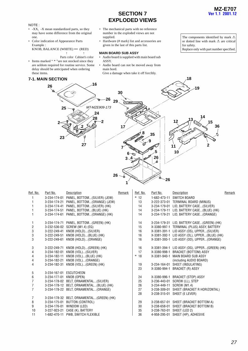
MZ-E707Ver 1.1 2001.12SECTION 7
EXPLODED VIEWSNOTE :• -XX, -X mean standardized parts, so they
may have some difference from the originalone.
• Color indication of Appearance PartsExample :KNOB, BALANCE (WHITE) ••• (RED)
↑ ↑Parts color Cabinet's color
• Items marked “ * ”are not stocked since theyare seldom required for routine service. Somedelay should be anticipated when orderingthese items.
• The mechanical parts with no referencenumber in the exploded views are notsupplied.
• Hardware (# mark) list and accessories aregiven in the last of this parts list.
Ref. No. Part No. Description Remark Ref. No. Part No. Description Remark
7-1. MAIN SECTION
The components identified by mark 0or dotted line with mark 0 are criticalfor safety.Replace only with part number specified.
1 3-234-174-01 PANEL, BOTTOM...(SILVER) (JEW)1 3-234-174-21 PANEL, BOTTOM...(ORANGE) (JEW)1 3-234-174-41 PANEL, BOTTOM...(SILVER) (HK)1 3-234-174-51 PANEL, BOTTOM...(BLUE) (HK)1 3-234-174-61 PANEL, BOTTOM...(ORANGE) (HK)
1 3-234-174-71 PANEL, BOTTOM...(GREEN) (HK)2 3-232-536-02 SCREW (M1.4) (EG)3 3-222-249-41 KNOB (HOLD)...(SILVER)3 3-222-249-51 KNOB (HOLD)...(BLUE) (HK)3 3-222-249-61 KNOB (HOLD)...(ORANGE)
3 3-222-249-71 KNOB (HOLD)...(GREEN) (HK)4 3-234-182-01 KNOB (VOL)...(SILVER)4 3-234-182-11 KNOB (VOL)...(BLUE) (HK)4 3-234-182-21 KNOB (VOL)...(ORANGE)4 3-234-182-31 KNOB (VOL)...(GREEN) (HK)
5 3-234-167-01 ESCUTCHEON6 3-234-177-01 KNOB (OPEN)7 3-234-178-02 BELT, ORNAMENTAL...(SILVER)7 3-234-178-12 BELT, ORNAMENTAL...(BLUE) (HK)7 3-234-178-22 BELT, ORNAMENTAL...(ORANGE)
7 3-234-178-32 BELT, ORNAMENTAL...(GREEN) (HK)8 3-234-175-01 BUTTON (CONTROL)9 3-234-176-01 WINDOW (LED)10 3-227-923-21 CASE (K), BATTERY11 1-682-470-11 PWB, SWITCH FLEXIBLE
* 12 1-682-473-11 SWITCH BOARD13 3-222-373-01 TERMINAL BOARD (MINUS)14 3-234-179-01 LID, BATTERY CASE...(SILVER)14 3-234-179-11 LID, BATTERY CASE...(BLUE) (HK)14 3-234-179-21 LID, BATTERY CASE...(ORANGE)
14 3-234-179-31 LID, BATTERY CASE...(GREEN) (HK)15 X-3380-997-1 TERMINAL (PLUS) ASSY, BATTERY16 X-3381-391-1 LID ASSY (OS), UPPER...(SILVER)16 X-3381-392-1 LID ASSY (OL), UPPER...(BLUE) (HK)16 X-3381-393-1 LID ASSY (OD), UPPER...(ORANGE)
16 X-3381-394-1 LID ASSY (OG), UPPER...(GREEN) (HK)17 X-3380-998-1 BRACKET (BOTTOM) ASSY
* 18 X-3381-940-1 MAIN BOARD SUB ASSY(including AUDIO BOARD)
19 3-234-164-01 SHEET (INSULATING)23 X-3380-994-1 BRACKET (R) ASSY
24 X-3380-996-1 BRACKET (STOP) ASSY25 3-236-443-01 SCREW (LL), STEP26 3-234-449-11 SCREW (M1.4)27 3-238-309-01 SHEET (BRACKET R HORIZONTAL)28 3-238-315-01 SHEET (E LEVER)
29 3-238-657-01 SHEET (BRACKET BOTTOM A)30 3-238-658-01 SHEET (BRACKET BOTTOM B)35 3-238-763-01 SHEET (LED 2)36 4-958-295-01 SHEET (HP), ADHESIVE
MT-MZE909-173
26
26
22
282
2
12
11
3 410
17
1
26
2626
67
9
8
27
23
1314
15
24
16
25
5
18
19
36
30
29
35
MAIN BOARD SUB ASSY• Audio board is supplied with main board sub
ASSY.• Audio board can not be moved away from
main bord. Give a damage when take it off forcibly.
28
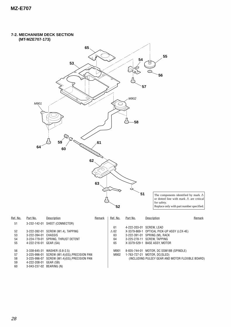
MZ-E707
Ref. No. Part No. Description Remark Ref. No. Part No. Description Remark
7-2. MECHANISM DECK SECTION (MT-MZE707-173)
The components identified by mark 0or dotted line with mark 0 are criticalfor safety.Replace only with part number specified.
64
65
M901
M902
5455
56
57
58
53
51
59
62
63
60
52
61
51 3-232-142-01 SHEET (CONNECTOR)
52 3-222-392-01 SCREW (M1.4), TAPPING53 3-222-394-01 CHASSIS54 3-224-779-01 SPRING, THRUST DETENT55 4-222-216-01 GEAR (SA)
56 3-338-645-31 WASHER (0.8-2.5)57 3-225-996-01 SCREW (M1.4)(EG),PRECISION PAN58 3-225-996-07 SCREW (M1.4)(EG),PRECISION PAN59 4-222-208-01 GEAR (SB)60 3-043-237-02 BEARING (N)
61 4-222-203-01 SCREW, LEAD062 X-3379-869-1 OPTICAL PICK-UP ASSY (LCX-4E)
63 3-222-391-01 SPRING (M), RACK64 3-225-278-11 SCREW, TAPPING65 X-3379-529-1 BASE ASSY, MOTOR
M901 8-835-744-01 MOTOR, DC SSM18B (SPINDLE)M902 1-763-727-21 MOTOR, DC(SLED)
(INCLUDING PULEEY GEAR AND MOTOR FLEXIBLE BOARD)
29
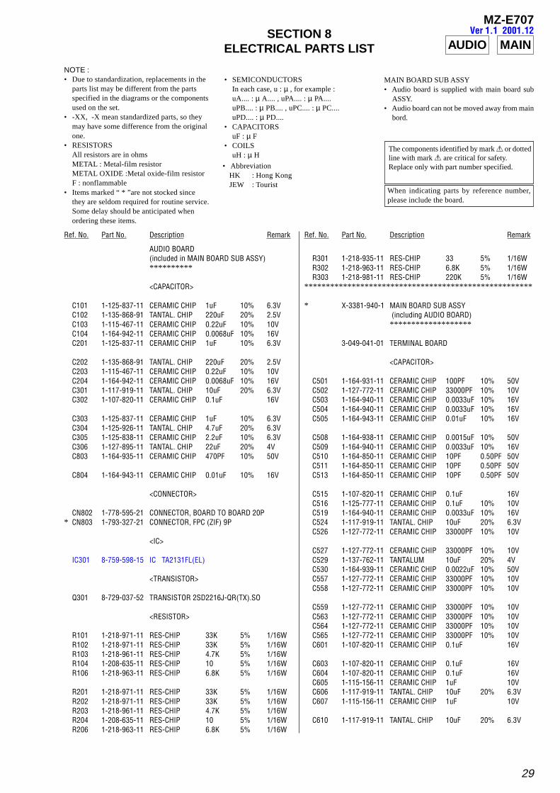
MZ-E707Ver 1.1 2001.12
NOTE :• Due to standardization, replacements in the
parts list may be different from the partsspecified in the diagrams or the componentsused on the set.
• -XX, -X mean standardized parts, so theymay have some difference from the originalone.
• RESISTORSAll resistors are in ohmsMETAL : Metal-film resistorMETAL OXIDE :Metal oxide-film resistorF : nonflammable
• Items marked “ * ”are not stocked sincethey are seldom required for routine service.Some delay should be anticipated whenordering these items.
• SEMICONDUCTORSIn each case, u : µ , for example :uA.... : µ A.... , uPA.... : µ PA....uPB.... : µ PB.... , uPC.... : µ PC....uPD.... : µ PD....
• CAPACITORSuF : µ F
• COILSuH : µ H
• AbbreviationHK : Hong KongJEW : Tourist
SECTION 8ELECTRICAL PARTS LIST
Ref. No. Part No. Description Remark Ref. No. Part No. Description Remark
AUDIO MAIN
AUDIO BOARD(included in MAIN BOARD SUB ASSY)**********
<CAPACITOR>
C101 1-125-837-11 CERAMIC CHIP 1uF 10% 6.3VC102 1-135-868-91 TANTAL. CHIP 220uF 20% 2.5VC103 1-115-467-11 CERAMIC CHIP 0.22uF 10% 10VC104 1-164-942-11 CERAMIC CHIP 0.0068uF 10% 16VC201 1-125-837-11 CERAMIC CHIP 1uF 10% 6.3V
C202 1-135-868-91 TANTAL. CHIP 220uF 20% 2.5VC203 1-115-467-11 CERAMIC CHIP 0.22uF 10% 10VC204 1-164-942-11 CERAMIC CHIP 0.0068uF 10% 16VC301 1-117-919-11 TANTAL. CHIP 10uF 20% 6.3VC302 1-107-820-11 CERAMIC CHIP 0.1uF 16V
C303 1-125-837-11 CERAMIC CHIP 1uF 10% 6.3VC304 1-125-926-11 TANTAL. CHIP 4.7uF 20% 6.3VC305 1-125-838-11 CERAMIC CHIP 2.2uF 10% 6.3VC306 1-127-895-11 TANTAL. CHIP 22uF 20% 4VC803 1-164-935-11 CERAMIC CHIP 470PF 10% 50V
C804 1-164-943-11 CERAMIC CHIP 0.01uF 10% 16V
<CONNECTOR>
CN802 1-778-595-21 CONNECTOR, BOARD TO BOARD 20P* CN803 1-793-327-21 CONNECTOR, FPC (ZIF) 9P
<IC>
IC301 8-759-598-15 IC TA2131FL(EL)
<TRANSISTOR>
Q301 8-729-037-52 TRANSISTOR 2SD2216J-QR(TX).SO
<RESISTOR>
R101 1-218-971-11 RES-CHIP 33K 5% 1/16WR102 1-218-971-11 RES-CHIP 33K 5% 1/16WR103 1-218-961-11 RES-CHIP 4.7K 5% 1/16WR104 1-208-635-11 RES-CHIP 10 5% 1/16WR106 1-218-963-11 RES-CHIP 6.8K 5% 1/16W
R201 1-218-971-11 RES-CHIP 33K 5% 1/16WR202 1-218-971-11 RES-CHIP 33K 5% 1/16WR203 1-218-961-11 RES-CHIP 4.7K 5% 1/16WR204 1-208-635-11 RES-CHIP 10 5% 1/16WR206 1-218-963-11 RES-CHIP 6.8K 5% 1/16W
R301 1-218-935-11 RES-CHIP 33 5% 1/16WR302 1-218-963-11 RES-CHIP 6.8K 5% 1/16WR303 1-218-981-11 RES-CHIP 220K 5% 1/16W
*****************************************************
* X-3381-940-1 MAIN BOARD SUB ASSY (including AUDIO BOARD)*******************
3-049-041-01 TERMINAL BOARD
<CAPACITOR>
C501 1-164-931-11 CERAMIC CHIP 100PF 10% 50VC502 1-127-772-11 CERAMIC CHIP 33000PF 10% 10VC503 1-164-940-11 CERAMIC CHIP 0.0033uF 10% 16VC504 1-164-940-11 CERAMIC CHIP 0.0033uF 10% 16VC505 1-164-943-11 CERAMIC CHIP 0.01uF 10% 16V
C508 1-164-938-11 CERAMIC CHIP 0.0015uF 10% 50VC509 1-164-940-11 CERAMIC CHIP 0.0033uF 10% 16VC510 1-164-850-11 CERAMIC CHIP 10PF 0.50PF 50VC511 1-164-850-11 CERAMIC CHIP 10PF 0.50PF 50VC513 1-164-850-11 CERAMIC CHIP 10PF 0.50PF 50V
C515 1-107-820-11 CERAMIC CHIP 0.1uF 16VC516 1-125-777-11 CERAMIC CHIP 0.1uF 10% 10VC519 1-164-940-11 CERAMIC CHIP 0.0033uF 10% 16VC524 1-117-919-11 TANTAL. CHIP 10uF 20% 6.3VC526 1-127-772-11 CERAMIC CHIP 33000PF 10% 10V
C527 1-127-772-11 CERAMIC CHIP 33000PF 10% 10VC529 1-137-762-11 TANTALUM 10uF 20% 4VC530 1-164-939-11 CERAMIC CHIP 0.0022uF 10% 50VC557 1-127-772-11 CERAMIC CHIP 33000PF 10% 10VC558 1-127-772-11 CERAMIC CHIP 33000PF 10% 10V
C559 1-127-772-11 CERAMIC CHIP 33000PF 10% 10VC563 1-127-772-11 CERAMIC CHIP 33000PF 10% 10VC564 1-127-772-11 CERAMIC CHIP 33000PF 10% 10VC565 1-127-772-11 CERAMIC CHIP 33000PF 10% 10VC601 1-107-820-11 CERAMIC CHIP 0.1uF 16V
C603 1-107-820-11 CERAMIC CHIP 0.1uF 16VC604 1-107-820-11 CERAMIC CHIP 0.1uF 16VC605 1-115-156-11 CERAMIC CHIP 1uF 10VC606 1-117-919-11 TANTAL. CHIP 10uF 20% 6.3VC607 1-115-156-11 CERAMIC CHIP 1uF 10V
C610 1-117-919-11 TANTAL. CHIP 10uF 20% 6.3V
When indicating parts by reference number,please include the board.
The components identified by mark 0 or dottedline with mark 0 are critical for safety.Replace only with part number specified.
MAIN BOARD SUB ASSY• Audio board is supplied with main board sub
ASSY.• Audio board can not be moved away from main
bord.
30
MZ-E707
Ref. No. Part No. Description Remark Ref. No. Part No. Description Remark
MAIN
@ Replacement of IC601 used in this set requires a special tool.
C613 1-164-935-11 CERAMIC CHIP 470PF 10% 50VC615 1-125-777-11 CERAMIC CHIP 0.1uF 10% 10V
C616 1-107-820-11 CERAMIC CHIP 0.1uF 16VC618 1-109-982-11 CERAMIC CHIP 1uF 10% 10VC699 1-164-943-11 CERAMIC CHIP 0.01uF 10% 16VC802 1-107-820-11 CERAMIC CHIP 0.1uF 16VC806 1-119-923-11 CERAMIC CHIP 0.047uF 10% 10V
C807 1-119-923-11 CERAMIC CHIP 0.047uF 10% 10VC810 1-164-943-11 CERAMIC CHIP 0.01uF 10% 16VC851 1-107-820-11 CERAMIC CHIP 0.1uF 16VC853 1-164-942-11 CERAMIC CHIP 0.0068uF 10% 16VC854 1-107-820-11 CERAMIC CHIP 0.1uF 16V
C901 1-137-739-11 TANTALUM 22uF 20% 6.3VC903 1-135-989-11 TANTAL. CHIP 47uF 20% 6.3VC904 1-135-837-11 TANTAL. CHIP 22uF 20% 6.3VC905 1-125-777-11 CERAMIC CHIP 0.1uF 10% 10VC907 1-109-982-11 CERAMIC CHIP 1uF 10% 10V
C908 1-164-940-11 CERAMIC CHIP 0.0033uF 10% 16VC909 1-164-943-11 CERAMIC CHIP 0.01uF 10% 16VC910 1-164-937-11 CERAMIC CHIP 0.001uF 10% 50VC911 1-117-919-11 TANTAL. CHIP 10uF 20% 6.3VC915 1-125-777-11 CERAMIC CHIP 0.1uF 10% 10V
C917 1-125-777-11 CERAMIC CHIP 0.1uF 10% 10VC918 1-125-777-11 CERAMIC CHIP 0.1uF 10% 10VC919 1-117-919-11 TANTAL. CHIP 10uF 20% 6.3VC920 1-125-777-11 CERAMIC CHIP 0.1uF 10% 10VC921 1-125-777-11 CERAMIC CHIP 0.1uF 10% 10V
C925 1-135-837-11 TANTAL. CHIP 22uF 20% 6.3VC952 1-128-964-11 TANTAL. CHIP 100uF 20% 6.3VC999 1-125-777-11 CERAMIC CHIP 0.1uF 10% 10V
<CONNECTOR>
* CN501 1-794-772-21 CONNECTOR, FPC (ZIF) 20P* CN551 1-778-156-11 CONNECTOR, FFC/FPC (ZIF) 8P
CN801 1-778-590-21 CONNECTOR, BOARD TO BOARD 20P
<DIODE>
D101 8-719-056-58 DIODE MAZS027008SOD201 8-719-056-58 DIODE MAZS027008SOD855 8-719-077-43 DIODE MAZZ068H01S0D901 8-719-081-33 DIODE MA2YD1500LS0D902 8-719-081-33 DIODE MA2YD1500LS0
D903 8-719-420-51 DIODE MA729
<FERRITE BEAD>
FB801 1-414-228-11 FERRITE 0uHFB802 1-414-228-11 FERRITE 0uH
<IC>
IC501 8-759-689-67 IC SN761057DBTIC551 6-700-680-01 IC SC111258FCR2
@ IC601 8-752-413-14 IC CXD2671-206GAIC801 8-759-680-85 IC AK6417AL-LIC901 8-759-698-61 IC XPC18A32FCR2
<JACK>
J301 1-793-288-62 JACK (i)
<INDUCTOR>
L503 1-469-570-21 INDUCTOR 10uHL901 1-419-258-21 INDUCTOR 68uHL902 1-419-646-21 INDUCTOR 47uHL904 1-414-398-11 INDUCTOR 10uHL905 1-412-032-11 INDUCTOR CHIP 100uH
<TRANSISTOR>
Q501 8-729-922-10 TRANSISTOR 2SA1577-QRQ801 8-729-429-44 TRANSISTOR XP1501Q803 8-729-037-75 TRANSISTOR UN9214J-(TX).SO
<RESISTOR>
R501 1-218-971-11 RES-CHIP 33K 5% 1/16WR503 1-218-953-11 RES-CHIP 1K 5% 1/16WR505 1-208-691-11 METAL CHIP 2.2K 1% 1/16WR515 1-208-691-11 METAL CHIP 2.2K 1% 1/16WR516 1-208-691-11 METAL CHIP 2.2K 1% 1/16W
R517 1-208-691-11 METAL CHIP 2.2K 1% 1/16WR519 1-218-977-11 RES-CHIP 100K 5% 1/16WR521 1-242-967-11 RES-CHIP 1 5% 1/16WR525 1-218-990-11 SHORT 0R526 1-218-990-11 SHORT 0
R601 1-208-635-11 RES-CHIP 10 5% 1/16WR602 1-208-635-11 RES-CHIP 10 5% 1/16WR603 1-218-943-11 RES-CHIP 150 5% 1/16WR605 1-218-965-11 RES-CHIP 10K 5% 1/16WR606 1-218-977-11 RES-CHIP 100K 5% 1/16W
R607 1-218-977-11 RES-CHIP 100K 5% 1/16WR609 1-218-981-11 RES-CHIP 220K 5% 1/16WR612 1-218-959-11 RES-CHIP 3.3K 5% 1/16WR613 1-218-945-11 RES-CHIP 220 5% 1/16WR614 1-218-953-11 RES-CHIP 1K 5% 1/16W
R615 1-202-974-11 RES-CHIP 3.3M 5% 1/16WR804 1-218-973-11 RES-CHIP 47K 5% 1/16WR806 1-218-977-11 RES-CHIP 100K 5% 1/16WR807 1-218-959-11 RES-CHIP 3.3K 5% 1/16WR808 1-218-959-11 RES-CHIP 3.3K 5% 1/16W
R817 1-218-941-11 RES-CHIP 100 5% 1/16WR818 1-218-941-11 RES-CHIP 100 5% 1/16WR819 1-218-989-11 RES-CHIP 1M 5% 1/16WR827 1-218-989-11 RES-CHIP 1M 5% 1/16WR830 1-218-975-11 RES-CHIP 68K 5% 1/16W
R831 1-218-947-11 RES-CHIP 330 5% 1/16WR832 1-218-935-11 RES-CHIP 33 5% 1/16WR833 1-218-967-11 RES-CHIP 15K 5% 1/16WR834 1-218-985-11 RES-CHIP 470K 5% 1/16WR835 1-218-985-11 RES-CHIP 470K 5% 1/16W
R839 1-218-949-11 RES-CHIP 470 5% 1/16WR903 1-218-957-11 RES-CHIP 2.2K 5% 1/16WR909 1-218-965-11 RES-CHIP 10K 5% 1/16WR910 1-218-965-11 RES-CHIP 10K 5% 1/16WR920 1-208-707-11 METAL CHIP 10K 1% 1/16W
R921 1-218-979-11 RES-CHIP 150K 5% 1/16WR946 1-208-715-11 METAL CHIP 22K 1% 1/16WR948 1-208-939-11 METAL CHIP 150K 1% 1/16WR950 1-218-953-11 RES-CHIP 1K 5% 1/16WR954 1-218-990-11 SHORT 0
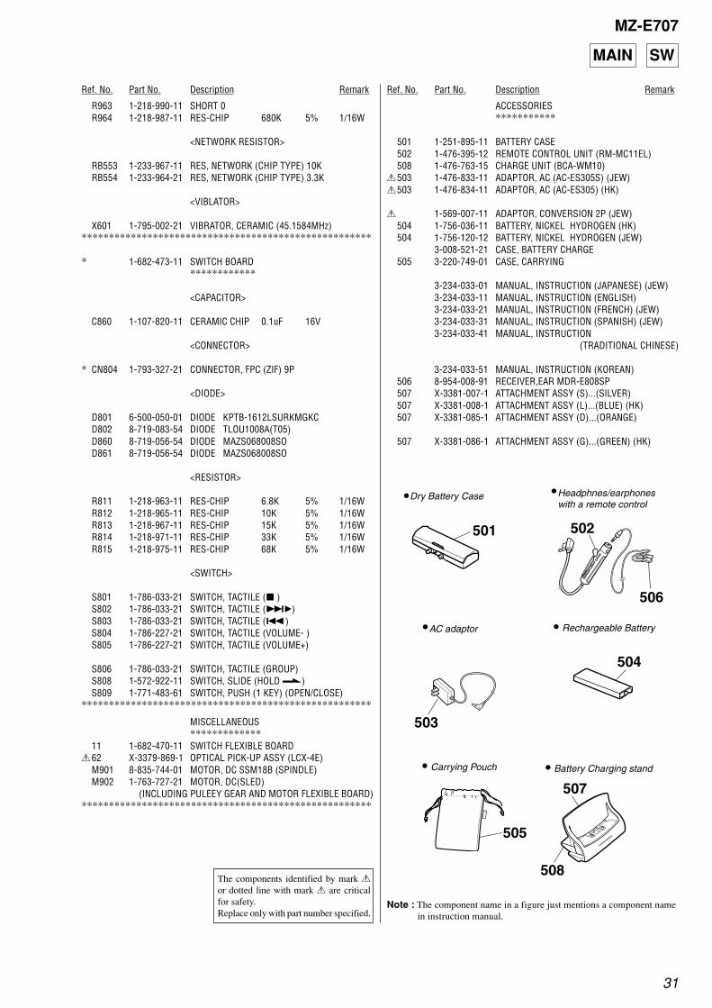
31
MZ-E707
Ref. No. Part No. Description Remark Ref. No. Part No. Description Remark
MAIN SW
R963 1-218-990-11 SHORT 0R964 1-218-987-11 RES-CHIP 680K 5% 1/16W
<NETWORK RESISTOR>
RB553 1-233-967-11 RES, NETWORK (CHIP TYPE) 10KRB554 1-233-964-21 RES, NETWORK (CHIP TYPE) 3.3K
<VIBLATOR>
X601 1-795-002-21 VIBRATOR, CERAMIC (45.1584MHz)*****************************************************
* 1-682-473-11 SWITCH BOARD************
<CAPACITOR>
C860 1-107-820-11 CERAMIC CHIP 0.1uF 16V
<CONNECTOR>
* CN804 1-793-327-21 CONNECTOR, FPC (ZIF) 9P
<DIODE>
D801 6-500-050-01 DIODE KPTB-1612LSURKMGKCD802 8-719-083-54 DIODE TLOU1008A(T05)D860 8-719-056-54 DIODE MAZS068008SOD861 8-719-056-54 DIODE MAZS068008SO
<RESISTOR>
R811 1-218-963-11 RES-CHIP 6.8K 5% 1/16WR812 1-218-965-11 RES-CHIP 10K 5% 1/16WR813 1-218-967-11 RES-CHIP 15K 5% 1/16WR814 1-218-971-11 RES-CHIP 33K 5% 1/16WR815 1-218-975-11 RES-CHIP 68K 5% 1/16W
<SWITCH>
S801 1-786-033-21 SWITCH, TACTILE (x )S802 1-786-033-21 SWITCH, TACTILE (>B)S803 1-786-033-21 SWITCH, TACTILE (.)S804 1-786-227-21 SWITCH, TACTILE (VOLUME- )S805 1-786-227-21 SWITCH, TACTILE (VOLUME+)
S806 1-786-033-21 SWITCH, TACTILE (GROUP)S808 1-572-922-11 SWITCH, SLIDE (HOLD .)S809 1-771-483-61 SWITCH, PUSH (1 KEY) (OPEN/CLOSE)
*****************************************************
Note : The component name in a figure just mentions a component namein instruction manual.
The components identified by mark 0or dotted line with mark 0 are criticalfor safety.Replace only with part number specified.
501
506
502
505
504
507
503
508
zDry Battery Case
z Rechargeable Battery
z Carrying Pouch z Battery Charging stand
zHeadphnes/earphoneswith a remote control
zAC adaptor
MISCELLANEOUS*************
11 1-682-470-11 SWITCH FLEXIBLE BOARD062 X-3379-869-1 OPTICAL PICK-UP ASSY (LCX-4E)
M901 8-835-744-01 MOTOR, DC SSM18B (SPINDLE)M902 1-763-727-21 MOTOR, DC(SLED)
(INCLUDING PULEEY GEAR AND MOTOR FLEXIBLE BOARD)*****************************************************
ACCESSORIES***********
501 1-251-895-11 BATTERY CASE502 1-476-395-12 REMOTE CONTROL UNIT (RM-MC11EL)508 1-476-763-15 CHARGE UNIT (BCA-WM10)
0503 1-476-833-11 ADAPTOR, AC (AC-ES305S) (JEW)0503 1-476-834-11 ADAPTOR, AC (AC-ES305) (HK)
0 1-569-007-11 ADAPTOR, CONVERSION 2P (JEW)504 1-756-036-11 BATTERY, NICKEL HYDROGEN (HK)504 1-756-120-12 BATTERY, NICKEL HYDROGEN (JEW)
3-008-521-21 CASE, BATTERY CHARGE505 3-220-749-01 CASE, CARRYING
3-234-033-01 MANUAL, INSTRUCTION (JAPANESE) (JEW)3-234-033-11 MANUAL, INSTRUCTION (ENGLISH)3-234-033-21 MANUAL, INSTRUCTION (FRENCH) (JEW)3-234-033-31 MANUAL, INSTRUCTION (SPANISH) (JEW)3-234-033-41 MANUAL, INSTRUCTION
(TRADITIONAL CHINESE)
3-234-033-51 MANUAL, INSTRUCTION (KOREAN)506 8-954-008-91 RECEIVER,EAR MDR-E808SP507 X-3381-007-1 ATTACHMENT ASSY (S)...(SILVER)507 X-3381-008-1 ATTACHMENT ASSY (L)...(BLUE) (HK)507 X-3381-085-1 ATTACHMENT ASSY (D)...(ORANGE)
507 X-3381-086-1 ATTACHMENT ASSY (G)...(GREEN) (HK)
MZ-E707
REVISION HISTORY
Clicking the version allows you to jump to the revised page.Also, clicking the version at the upper right on the revised page allows you to jump to the next revisedpage.
Ver. Date Description of Revision
1.1 2001.12 Change the main board to service ASSY (including audio board). (SPM-01053)
1.0 2001.10 New