MZ-R70 - Minidisc Community...
51
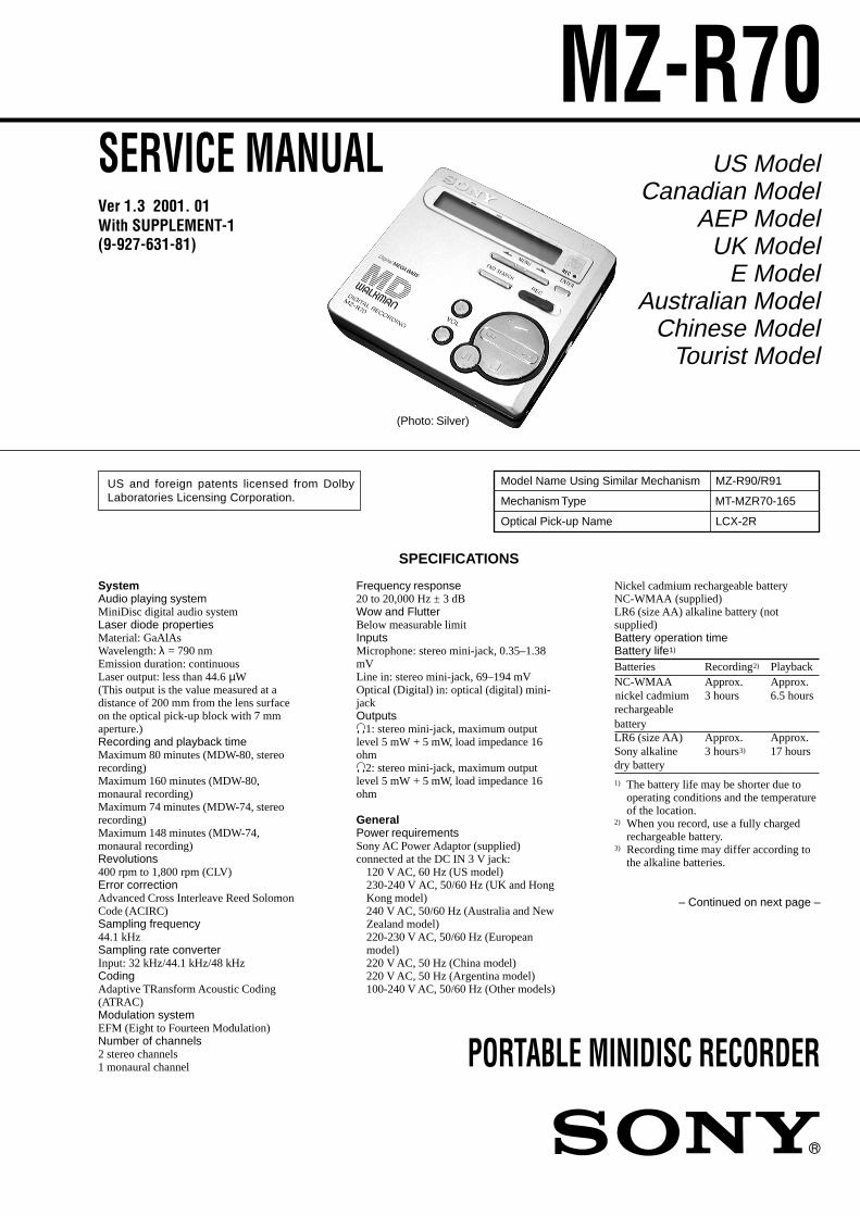
MZ-R70 SERVICE MANUAL PORTABLE MINIDISC RECORDER Model Name Using Similar Mechanism MZ-R90/R91 Mechanism Type MT-MZR70-165 Optical Pick-up Name LCX-2R (Photo: Silver) System Audio playing system MiniDisc digital audio system Laser diode properties Material: GaAlAs Wavelength: λ = 790 nm Emission duration: continuous Laser output: less than 44.6 µW (This output is the value measured at a distance of 200 mm from the lens surface on the optical pick-up block with 7 mm aperture.) Recording and playback time Maximum 80 minutes (MDW-80, stereo recording) Maximum 160 minutes (MDW-80, monaural recording) Maximum 74 minutes (MDW-74, stereo recording) Maximum 148 minutes (MDW-74, monaural recording) Revolutions 400 rpm to 1,800 rpm (CLV) Error correction Advanced Cross Interleave Reed Solomon Code (ACIRC) Sampling frequency 44.1 kHz Sampling rate converter Input: 32 kHz/44.1 kHz/48 kHz Coding Adaptive TRansform Acoustic Coding (ATRAC) Modulation system EFM (Eight to Fourteen Modulation) Number of channels 2 stereo channels 1 monaural channel SPECIFICATIONS Frequency response 20 to 20,000 Hz ± 3 dB Wow and Flutter Below measurable limit Inputs Microphone: stereo mini-jack, 0.35–1.38 mV Line in: stereo mini-jack, 69–194 mV Optical (Digital) in: optical (digital) mini- jack Outputs i1: stereo mini-jack, maximum output level 5 mW + 5 mW, load impedance 16 ohm i2: stereo mini-jack, maximum output level 5 mW + 5 mW, load impedance 16 ohm General Power requirements Sony AC Power Adaptor (supplied) connected at the DC IN 3 V jack: 120 V AC, 60 Hz (US model) 230-240 V AC, 50/60 Hz (UK and Hong Kong model) 240 V AC, 50/60 Hz (Australia and New Zealand model) 220-230 V AC, 50/60 Hz (European model) 220 V AC, 50 Hz (China model) 220 V AC, 50 Hz (Argentina model) 100-240 V AC, 50/60 Hz (Other models) Nickel cadmium rechargeable battery NC-WMAA (supplied) LR6 (size AA) alkaline battery (not supplied) Battery operation time Battery life 1) Batteries Recording 2) Playback NC-WMAA Approx. Approx. nickel cadmium 3 hours 6.5 hours rechargeable battery LR6 (size AA) Approx. Approx. Sony alkaline 3 hours 3) 17 hours dry battery 1) The battery life may be shorter due to operating conditions and the temperature of the location. 2) When you record, use a fully charged rechargeable battery. 3) Recording time may differ according to the alkaline batteries. – Continued on next page – US Model Canadian Model AEP Model UK Model E Model Australian Model Chinese Model Tourist Model US and foreign patents licensed from Dolby Laboratories Licensing Corporation. Ver 1.3 2001. 01 With SUPPLEMENT-1 (9-927-631-81)
Transcript of MZ-R70 - Minidisc Community...
– 1 –
MZ-R70SERVICE MANUAL
PORTABLE MINIDISC RECORDER
Model Name Using Similar Mechanism MZ-R90/R91
Mechanism Type MT-MZR70-165
Optical Pick-up Name LCX-2R
(Photo: Silver)
SystemAudio playing systemMiniDisc digital audio systemLaser diode propertiesMaterial: GaAlAsWavelength: λ = 790 nmEmission duration: continuousLaser output: less than 44.6 µW(This output is the value measured at adistance of 200 mm from the lens surfaceon the optical pick-up block with 7 mmaperture.)Recording and playback timeMaximum 80 minutes (MDW-80, stereorecording)Maximum 160 minutes (MDW-80,monaural recording)Maximum 74 minutes (MDW-74, stereorecording)Maximum 148 minutes (MDW-74,monaural recording)Revolutions400 rpm to 1,800 rpm (CLV)Error correctionAdvanced Cross Interleave Reed SolomonCode (ACIRC)Sampling frequency44.1 kHzSampling rate converterInput: 32 kHz/44.1 kHz/48 kHzCodingAdaptive TRansform Acoustic Coding(ATRAC)Modulation systemEFM (Eight to Fourteen Modulation)Number of channels2 stereo channels1 monaural channel
SPECIFICATIONS
Frequency response20 to 20,000 Hz ± 3 dBWow and FlutterBelow measurable limitInputsMicrophone: stereo mini-jack, 0.35–1.38mVLine in: stereo mini-jack, 69–194 mVOptical (Digital) in: optical (digital) mini-jackOutputsi1: stereo mini-jack, maximum outputlevel 5 mW + 5 mW, load impedance 16ohmi2: stereo mini-jack, maximum outputlevel 5 mW + 5 mW, load impedance 16ohm
GeneralPower requirementsSony AC Power Adaptor (supplied)connected at the DC IN 3 V jack:
120 V AC, 60 Hz (US model)230-240 V AC, 50/60 Hz (UK and HongKong model)240 V AC, 50/60 Hz (Australia and NewZealand model)220-230 V AC, 50/60 Hz (Europeanmodel)220 V AC, 50 Hz (China model)220 V AC, 50 Hz (Argentina model)100-240 V AC, 50/60 Hz (Other models)
Nickel cadmium rechargeable batteryNC-WMAA (supplied)LR6 (size AA) alkaline battery (notsupplied)Battery operation timeBattery life1)
Batteries Recording2) PlaybackNC-WMAA Approx. Approx.nickel cadmium 3 hours 6.5 hoursrechargeablebatteryLR6 (size AA) Approx. Approx.Sony alkaline 3 hours3) 17 hoursdry battery
1) The battery life may be shorter due tooperating conditions and the temperatureof the location.
2) When you record, use a fully chargedrechargeable battery.
3) Recording time may differ according tothe alkaline batteries.
– Continued on next page –
US ModelCanadian Model
AEP ModelUK Model
E ModelAustralian Model
Chinese ModelTourist Model
US and foreign patents licensed from DolbyLaboratories Licensing Corporation.
Ver 1.3 2001. 01With SUPPLEMENT-1(9-927-631-81)
– 2 –
Flexible Circuit Board Repairing• Keep the temperature of the soldering iron around 270°C
during repairing.• Do not touch the soldering iron on the same conductor of the
circuit board (within 3 times).• Be careful not to apply force on the conductor when soldering
or unsoldering.
Notes on chip component replacement• Never reuse a disconnected chip component.• Notice that the minus side of a tantalum capacitor may be
damaged by heat.
CAUTIONUse of controls or adjustments or performance of proceduresother than those specified herein may result in hazardousradiation exposure.
IN NO EVENT SHALL SELLER BELIABLE FOR ANY DIRECT,INCIDENTAL OR CONSEQUENTIALDAMAGES OF ANY NATURE, ORLOSSES OR EXPENSES RESULTINGFROM ANY DEFECTIVE PRODUCTOR THE USE OF ANY PRODUCT.
“MD WALKMAN” is a trademark of SonyCorporation.
This MiniDisc player is classi-fied as a CLASS 1 LASERproduct.The CLASS 1 LASERPRODUCT label is located onthe bottom exterior.
DimensionsApprox. 81 × 74 × 26.2 mm (w/h/d)(3 1/4 × 3 × 1 1/16 in.) without projections.MassApprox. 115 g (4 oz) the recorder onlyApprox. 155 g (5.4 oz) incl. a recordableMD, and NC-WMAA nickel cadmiumrechargeable batterySupplied accessoriesAC power adaptor (1)Headphones with a remote control (1)Optical cable (1)NC-WMAA nickel cadmium rechargeablebattery (1)Rechargeable battery carrying case (1)Carrying pouch (1)
Design and specifications are subject to changewithout notice.
SAFETY-RELATED COMPONENT WARNING!!
COMPONENTS IDENTIFIED BY MARK 0 OR DOTTED LINEWITH MARK 0 ON THE SCHEMATIC DIAGRAMS AND INTHE PARTS LIST ARE CRITICAL TO SAFE OPERATION.REPLACE THESE COMPONENTS WITH SONY PARTS WHOSEPART NUMBERS APPEAR AS SHOWN IN THIS MANUALOR IN SUPPLEMENTS PUBLISHED BY SONY.
ATTENTION AU COMPOSANT AYANT RAPPORT À LA SÉCURITÉ!!
LES COMPOSANTS IDENTIFIÉS PAR UNE MARQUE 0 SUR LESDIAGRAMMES SCHÉMATIQUES ET LA LISTE DES PIÈCESSONT CRITIQUES POUR LA SÉCURITÉ DE FONCTIONNEMENT.NE REMPLACER CES COMPOSANTS QUE PAR DES PIÈCESSONY DONT LES NUMÉROS SONT DONNÉS DANS CE MANUELOU DANS LES SUPPLÉMENTS PUBLIÉS PAR SONY.
– 3 –
1. SERVICING NOTE ......................................................... 4
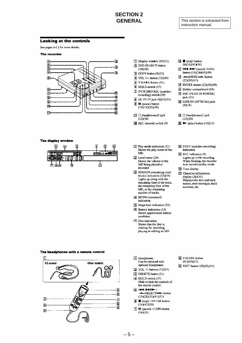
2. GENERAL ......................................................................... 5Looking at the Controls ........................................................ 5Recording an MD Right Away! ............................................ 6Playing an MD Right Away! ................................................. 7
3. DISASSEMBLY ............................................................... 83-1. Block Assy, Bottom .............................................................. 83-2. Panel Block Assy, Upper ....................................................... 83-3. LCD Module ......................................................................... 93-4. Main Board ........................................................................... 93-5. MD Mechanism Deck ......................................................... 103-6. Service Assy, OP ................................................................. 103-7. Holder Assy ......................................................................... 113-8. Motor Flexible Board .......................................................... 113-9. Motor, DC (M602) .............................................................. 123-10. “Motor, DC (M601)”, “Motor, DC (M603)” .................... 12
4. TEST MODE ................................................................... 134-1. Outline ................................................................................. 134-2. Test Mode ............................................................................ 134-3. Manual Mode ...................................................................... 144-4. Overall Adjustment Mode ................................................... 154-5. Sound Skip Check Result Display Mode ............................ 164-6. Self-diagnosis Display Mode .............................................. 174-7. Key Check Mode ................................................................. 19
TABLE OF CONTENTS
5. ELECTRICAL ADJUSTMENTS .............................. 205-1. Outline ................................................................................. 205-2. Precautions for Adjustment ................................................. 205-3. Adjustment Sequence .......................................................... 205-4. NV Reset ............................................................................. 205-5. Power Supply Manual Adjustment ...................................... 205-6. Temperature Correction ....................................................... 225-7. Overall Adjustment Mode ................................................... 225-8. Laser Power Check ............................................................. 23
6. DIAGRAMS ..................................................................... 256-1. Block Diagram – MD Section – .......................................... 256-2. Block Diagram – Audio Section – ...................................... 276-3. Block Diagram – Power Supply Section – .......................... 296-4. Printed Wiring Board – Main Board – ................................ 316-5. Schematic Diagram – Main Board (1/3) – .......................... 356-6. Schematic Diagram – Main Board (2/3) – .......................... 376-7. Schematic Diagram – Main Board (3/3) – .......................... 396-8. IC Block Diagrams.............................................................. 416-9. IC Pin Descriptions ............................................................. 44
7. EXPLODED VIEWS ..................................................... 517-1. Cabinet Section ................................................................... 517-2. Mechanism Deck Section ................................................... 52
8. ELECTRICAL PARTS LIST ...................................... 53
– 4 –
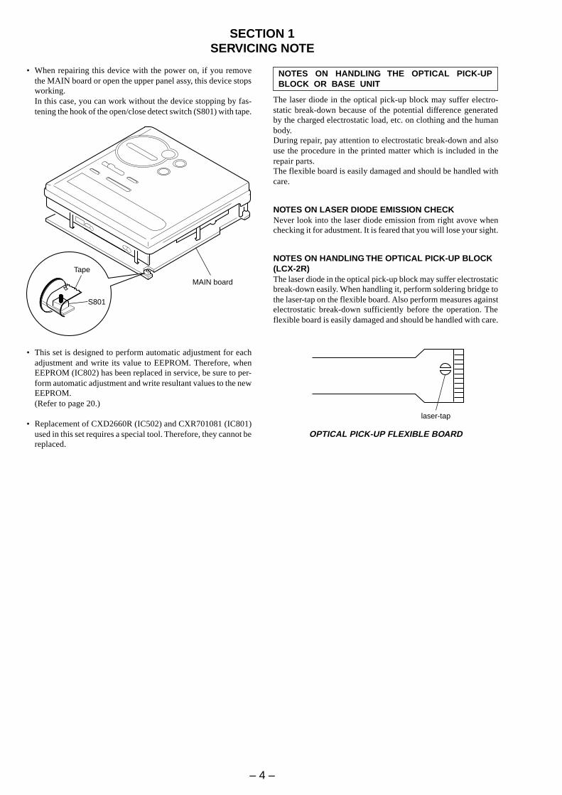
SECTION 1SERVICING NOTE
NOTES ON HANDLING THE OPTICAL PICK-UPBLOCK OR BASE UNIT
The laser diode in the optical pick-up block may suffer electro-static break-down because of the potential difference generatedby the charged electrostatic load, etc. on clothing and the humanbody.During repair, pay attention to electrostatic break-down and alsouse the procedure in the printed matter which is included in therepair parts.The flexible board is easily damaged and should be handled withcare.
NOTES ON LASER DIODE EMISSION CHECKNever look into the laser diode emission from right avove whenchecking it for adustment. It is feared that you will lose your sight.
NOTES ON HANDLING THE OPTICAL PICK-UP BLOCK(LCX-2R)The laser diode in the optical pick-up block may suffer electrostaticbreak-down easily. When handling it, perform soldering bridge tothe laser-tap on the flexible board. Also perform measures againstelectrostatic break-down sufficiently before the operation. Theflexible board is easily damaged and should be handled with care.
OPTICAL PICK-UP FLEXIBLE BOARD
• When repairing this device with the power on, if you removethe MAIN board or open the upper panel assy, this device stopsworking.In this case, you can work without the device stopping by fas-tening the hook of the open/close detect switch (S801) with tape.
• This set is designed to perform automatic adjustment for eachadjustment and write its value to EEPROM. Therefore, whenEEPROM (IC802) has been replaced in service, be sure to per-form automatic adjustment and write resultant values to the newEEPROM.(Refer to page 20.)
• Replacement of CXD2660R (IC502) and CXR701081 (IC801)used in this set requires a special tool. Therefore, they cannot bereplaced.
laser-tap
Tape
S801
MAIN board
– 5 –
SECTION 2GENERAL This section is extracted from
instruction manual.
– 6 –
– 7 –
– 8 –
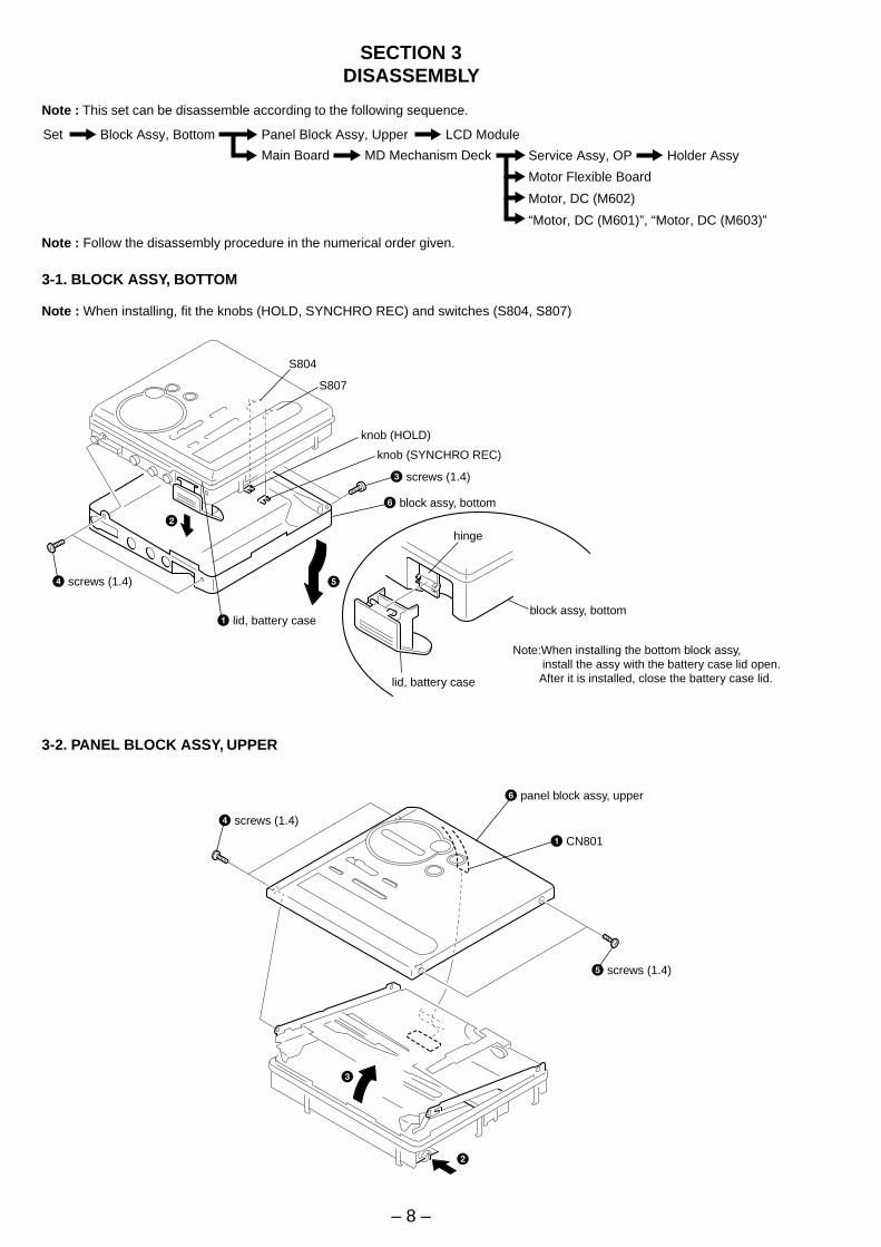
Note : This set can be disassemble according to the following sequence.
SECTION 3DISASSEMBLY
3-1. BLOCK ASSY, BOTTOM
3-2. PANEL BLOCK ASSY, UPPER
Note : Follow the disassembly procedure in the numerical order given.
Set Block Assy, Bottom Panel Block Assy, Upper LCD Module
Main Board MD Mechanism Deck Service Assy, OP
Motor Flexible Board
Holder Assy
Motor, DC (M602)
“Motor, DC (M601)”, “Motor, DC (M603)”
1 CN801
2
3
4 screws (1.4)
5 screws (1.4)
6 panel block assy, upper
Note : When installing, fit the knobs (HOLD, SYNCHRO REC) and switches (S804, S807)
1 lid, battery case
lid, battery case
6 block assy, bottom
block assy, bottom
3 screws (1.4)
knob (HOLD)
knob (SYNCHRO REC)
hinge
S807
S804
4 screws (1.4)
2
5
Note:When installing the bottom block assy, install the assy with the battery case lid open. After it is installed, close the battery case lid.
– 9 –
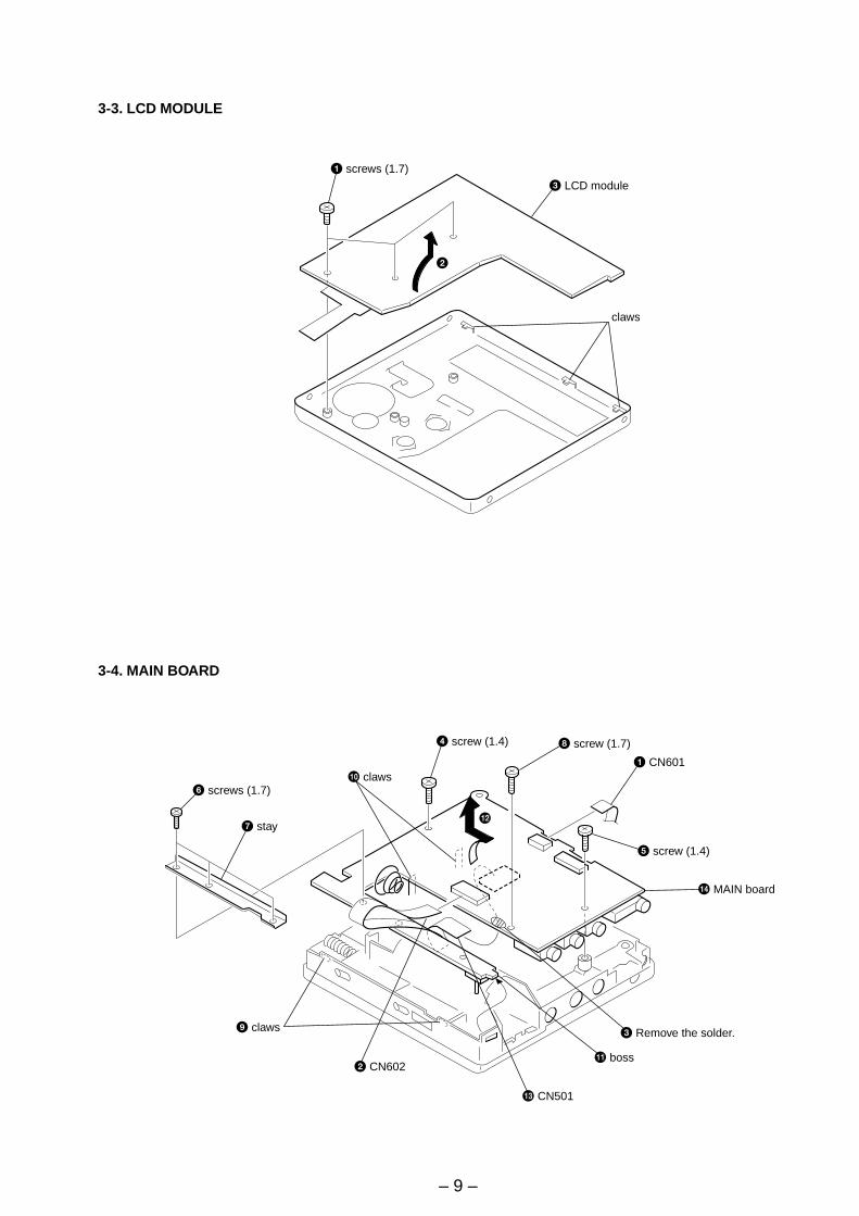
3-3. LCD MODULE
3-4. MAIN BOARD
1 screws (1.7)
3 LCD module
claws
2
4 screw (1.4)
qs
5 screw (1.4)
8 screw (1.7)
6 screws (1.7)
7 stay
1 CN601
qd CN501
3 Remove the solder.
qa boss
qf MAIN board
2 CN602
9 claws
0 claws
– 10 –
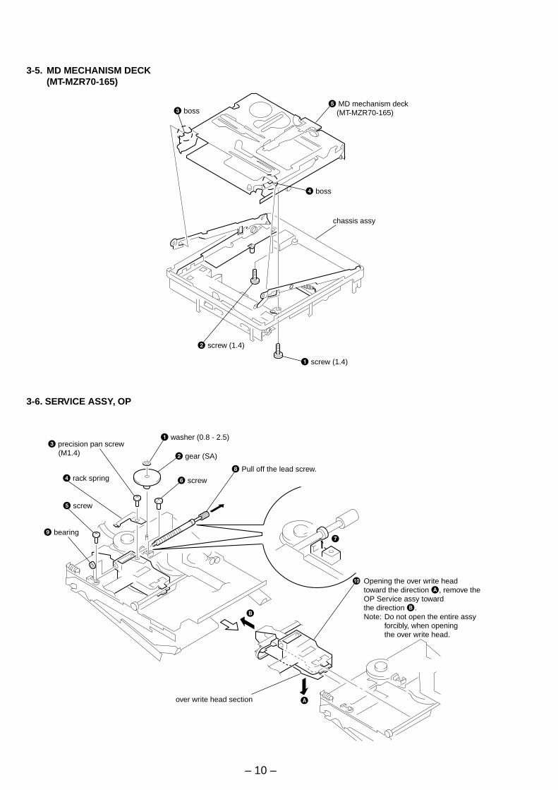
3-5. MD MECHANISM DECK(MT-MZR70-165)
3-6. SERVICE ASSY, OP
3 boss
4 boss
chassis assy
5 MD mechanism deck (MT-MZR70-165)
1 screw (1.4)
2 screw (1.4)
9 bearing
5 screw
4 rack spring
3 precision pan screw (M1.4)
1 washer (0.8 - 2.5)
2 gear (SA)
6 screw
8 Pull off the lead screw.
7
B
A
0 Opening the over write head toward the direction A, remove theOP Service assy toward the direction B.Note: Do not open the entire assy
forcibly, when opening the over write head.
over write head section
– 11 –
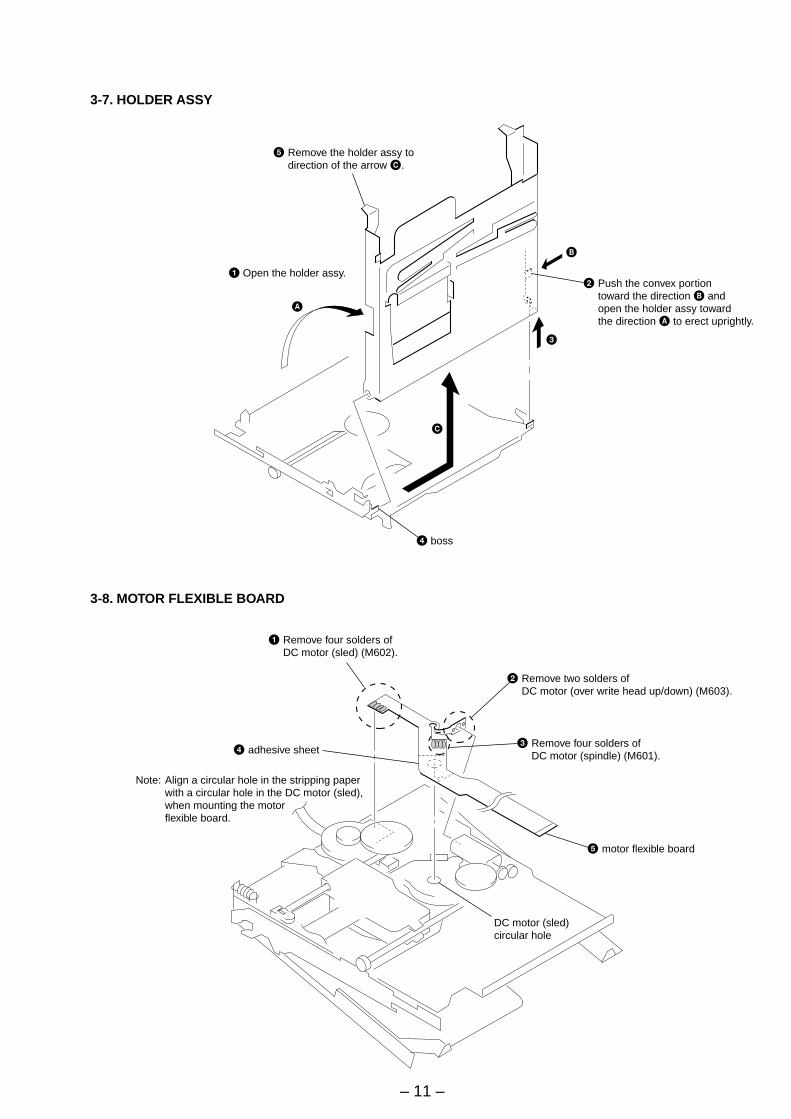
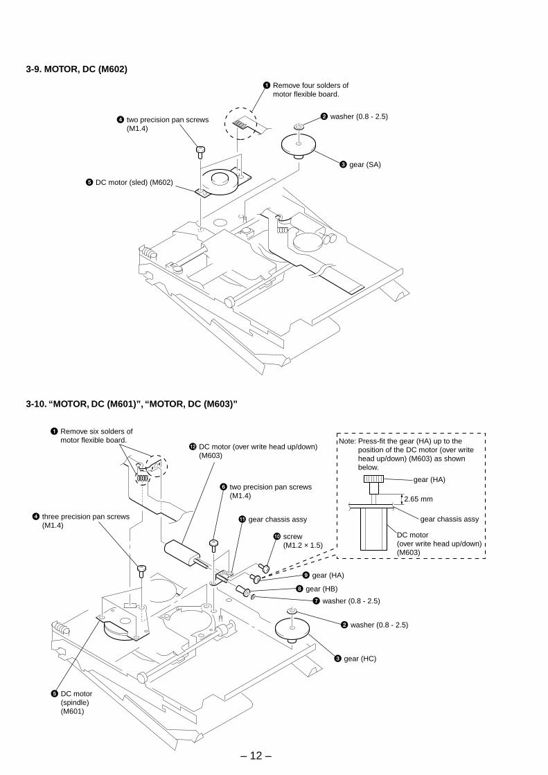
3-7. HOLDER ASSY
2 Remove two solders of DC motor (over write head up/down) (M603).
1 Remove four solders of DC motor (sled) (M602).
3 Remove four solders of DC motor (spindle) (M601).
DC motor (sled) circular hole
5 motor flexible board
4 adhesive sheet
Note: Align a circular hole in the stripping paperwith a circular hole in the DC motor (sled),when mounting the motor flexible board.
3-8. MOTOR FLEXIBLE BOARD
5 Remove the holder assy to direction of the arrow C.
1 Open the holder assy.
A
B
3
C
2 Push the convex portion toward the direction B and open the holder assy towardthe direction A to erect uprightly.
4 boss
– 12 –
4 two precision pan screws(M1.4)
5 DC motor (sled) (M602)
1 Remove four solders of motor flexible board.
2 washer (0.8 - 2.5)
3 gear (SA)
1 Remove six solders of motor flexible board.
4 three precision pan screws(M1.4)
qs DC motor (over write head up/down) (M603)
6 two precision pan screws(M1.4)
qa gear chassis assy
0 screw(M1.2 × 1.5)
9 gear (HA)
8 gear (HB)
7 washer (0.8 - 2.5)
2 washer (0.8 - 2.5)
3 gear (HC)
5 DC motor (spindle)(M601)
DC motor(over write head up/down)(M603)
gear chassis assy
gear (HA)
2.65 mm
Note: Press-fit the gear (HA) up to the position of the DC motor (over writehead up/down) (M603) as shown below.
3-9. MOTOR, DC (M602)
3-10. “MOTOR, DC (M601)”, “MOTOR, DC (M603)”
– 13 –
IC502
FB50
1
C530
2526283236147
118116
119120
117114113 112
115
110109 111104108 106104105 103101102 100
144 14637 46 47 50 53 56 59 64 6842 45 48 51 55 57 60 63 66 67
145
88
88 87 86 83 81 78 74 72 69 64 63 60 5890 89 85 84 80 77 75 71 68 65 62 59 5793 92 9196 95 9499 98 97
82 79 76 73 70 67 66 61 55 5652 53 5449 50 5146 47 4843 45 4440 41 4237 36 3934 35 36
32 3326 28 3125 29 30
19 22 2721 2320 24
10 13 1611 14 1712 15 18
742 6 8
1 3 5 9
8582787673
89868380
90878481
777472
7975
43 44 49 52 54 58 61 62 65 697071
38 4039 41
AP508AP504
AP505R530R529
C529
S804HOLD
AP1001
L502FB503FB502
FB504
BP801
AP519
AP830
AP521
OFF ON
R506
R503
R508
R509
R510
C537
R935
AP5209
AP806C801 AP911
AP807AP907
AP834AP517X801
AP511AP51612
09AP506
10
32
AP80
4AP
803
AP507
805
IC802
IC801
8 1
5 4
– MAIN BOARD (SIDE B) –
BP801
SECTION 4TEST MODE
4-1. OUTLINE• This set provides the Overall adjustment mode (Assy mode) that
allows CD and MO disc to be automatically adjusted when inthe test mode. In this overall adjustment mode, the protect switchis detected to judge the disc, CD or MO, and each adjustment isautomatically executed in order. If a fault is found, the systemdisplays its location. Also, the manual mode allows each indi-vidual adjustment to be automatically adjusted.
• The keys in the description refer to the keys on both set andremote commander unless otherwise specified. Though LCDdisplay shows the LCD of the remote commander, same con-tents are also displayed on the LCD of the set.
4-2. TEST MODE4-2-1. Setting Method of Test ModeThere are two different methods to set the test mode:1 Short BP801 (TEST) on the MAIN board with a solder bridge
(connect pin y; of IC801 to the ground). Then, turn on thepower.
2 In the normal mode, turn on the HOLD switch on the set. Whilepressing the x key on the set, press the following remotecontrol keys in the following order:
> t > t . t . t > t . t > t . t X t X
4-2-2. Operation in Setting the Test Mode• When the test mode becomes active, first the display check mode
is selected. (Press x key once, when the display check modeis not active.)
• Other mode can be selected from the display check mode.• When the test mode is set, the LCD repeats the following dis-
play.
LCD display
• When the X key is pressed and hold down, the display at thattime is held so that display can be checked.
4-2-3. Releasing the Test ModeFor test mode set with the method 1:Turn off the power and open the solder bridge on BP801 (TEST)on the MAIN board.Note: Remove the solders completely. Remaining could be shorted with
the chassis, etc.For test mode set with the method 2:Turn off the power.Note: If electrical adjustment (see page 20) has not been finished com-
pletely, always start in the test mode. (The set cannot start in nor-mal mode.)
Microprocessorversiondisplay
All off
All lit xxxxxxxxx
V0.000
888
001
F1SHUF
REC
– 14 –
4-2-4. Configuration of Test Mode
Note: *1) on the set*2) on the remote commander*3) on the set or remote commander
4-3. MANUAL MODEMode to adjust or check the operation of the set by function.Normally, the adjustment in this mode is not executed.• Transition method in Manual Mode1. Setting the test mode. (See page 13)2. Press the > or [VOL +] key activates the manual mode
where the LCD display as shown below.
3. The optical pick-up moves outward or inward whilethe > or . key is pressed for several seconds respec-tively.
4. Each test item is assigned with a 3-digit mode number;100th place is a major item, 10th place is a medium item, andunit place is a minor item.
[Manual Mode]
[Servo Mode][Audio Mode][Power Mode]
[OP Alignment Mode]
[Overall Adjustment Mode]
[Self-Diagnosis Display Mode]
Press the > *1) or [VOL +] *3) key
[Key Check Mode]
[Test Mode $Display Check Mode%]
Press the x *3) key
Press the x *3) key
Press the x *3) key
Press the x *3) key
Press the . *3) or [VOL --] *3) key
Press the N *1) or [REC] *1) or N > *2) key
press the [DISPLAY] *2) or MENU . *1) key
Press the [T MARK] *3) or [DISPLAY] *2) key on the remote commander for several seconds.
Quit the key check or open the upper panel
[Sound Skip Check Result Display Mode]
LCD display
M a n u a l000
[VOL +] key:100th place of mode number increase.
[VOL --] key:100th place of mode number decrease.
[Major item switching]
[VOL +] key:10th place of mode number increase.
[VOL --] key:10th place of mode number decrease.
[VOL +] key:Increases the adjusted value
[VOL --] key:Decreases the adjusted value
[Medium item switching]
N key x key
[Minor item switching]
[Adjusted value variation]
X key: When adjusted value is changed:Adjusted value is written.When adjusted value is not changed:That item is adjusted automatically.
[Adjusted value write]
N key
N key: Unit place of mode number increase.
x key
– 15 –
5. The display changes a shown below each time the jog key onthe set is turned up or [DISPLAY] key on the remote com-mander is pressed.
However in the power mode (mode number 700’s), only thepower adjustment value is displayed.
6. Quit the manual mode, and press x key to return to the testmode (display check mode).
A D 8 5731
• Power Supply Adjusted Value
LCD display
mode numberfixed display
adjusted value
4-4. OVERALL ADJUSTMENT MODEMode to adjust the servo automatically in all items.Normally, automatic adjustment is executed in this mode at therepair.Adjust the CD first, when performing adjustment.• Configuration of overall adjustment
For further information, refer to the Section 5 Electrical Adjust-ment. (See page 20)
• Address & Adjusted Value Display
LCD display
• Jitter Value & Adjusted Value Display
LCD display
• Block Error Value & Adjusted Value Display
LCD display
• ADIP Error Value & Adjusted Value Display
LCD display
• Item Title Display
LCD display
C 6 8 S 0 1011
0 6 3 B 0 1011
0 5 9 A 0 1011
L r e f P w 0 1011
0 F F J 0 1011
mode numberaddress
adjusted value
mode numberjitter value
adjusted value
mode numberblock error value
adjusted value
mode numberADIP error value
adjusted value
adjusted valuemode number
item title
> key . key
> key
Titledisplay
CD overalladjusting
CD overalladjustment
OK
MO overalladjusting
MO overalladjustment
OK
CD overalladjustment
NG
MO overalladjustment
NG
N keyprotect switch ON
All item OK
protect switch OFF
NG item existsor x key
NG item existsor x key
x key
x key
x key
x key
[Test mode $display check mode%]
– 16 –
4. When [REC] key on the set is pressed, the total of error countis displayed on the LCD, and each time the > key is pressed,the error count descents one by one as shown below. Also,when . key is pressed, the error count ascends by one.If N key is pressed, the error count during play is displayed.
** : Sound skip check items counter (hexadecimal)###### : 6-digit address (hexadecimal) where a sound skipped
last
Error code
Cause of error Description of error
EIB Sound error correction error
PlaybackStat Decorder status error
Adrs Cannot access the address
BEmp Buffer becomes empty
BOvr Buffer becomes full and sounds aredumped
Recording Bful Buffer capacity lowers and data areforcibly written
Rtry Retry count over
5. Quit the sound skip check result display mode, and pressthe x key to return to the test mode (display check mode).
4-5. SOUND SKIP CHECK RESULT DISPLAY MODEThis set can display and check the error count occurring duringrecord and play.
• Setting method of Sound Skip Check Result DisplayMode
1. Setting the test mode. (See page 13)2. Press the N or [REC] key on the set activates the sound skip
check result display mode where the LCD displays as shownbelow.When N or [REC] key on the set is pressed:
3. When N key or N > key on the remote commander ispressed, the total of error count is displayed on the LCD, andeach time the > key is pressed, the error count descentsone by one as shown below. Also, when . key is pressed,the error count ascends by one. If [REC] key on the set ispressed, the error count during record is displayed.
** : Sound skip check items counter (hexadecimal)###### : 6-digit address (hexadecimal) where a sound skipped
last
LCD display
P * * R * *000
Total of play system error count
Total of record system error count
S t a t * *000
A d r s * *000
B E m p * *000
# # # # # #000
P * * R * *000
E I B * *000
B f u l * *000
R t r y * *000
# # # # # #000
P * * R * *000
B O v r * *000
– 17 –
4-6. SELF-DIAGNOSIS DISPLAY MODE• This set uses the self-diagnosis system in which if an error oc-
curs in recording/playback mode, the error is detected by themodel control and power control blocks of the microprocessorand information on the cause is stored as history in EEPROM.By viewing this history in test mode, it helps you to analyze afault and determine its location.Total recording time has been recorded as optical pick-up usingtime, and it is compared with the total recording time in theself-diagnosis display mode to find when an error occurred.Clear both total recording time and the time in self-diagnosisdisplay mode, when the optical pick-up was replaced.
1. Setting the test mode. (See page 13)2. Press the MENU . key on the set or press the [DISPLAY]
key on the remote commander activates the self-diagnosis dis-play mode where the LCD display as shown below.
3. Then, each time > key is pressed, LCD display descendsby one as shown below. Also, the LCD display ascends by onewhen . key is pressed.
4. Quit the self-diagnosis display mode, and press the x key toreturn to the test mode (display check mode).
LCD display
* * : Self-Diagnosis Data
1 s t 0 * *000
history code
1 s t 0 * *000
1 s t 1 * *000
1 s t 2 * *000
N 0 * *000
N 1 * *000
N 2 * *000
N - 1 0 * *000
N - 1 1 * *000
N - 1 2 * *000
N - 2 0 * *000
N - 2 1 * *000
N - 2 2 * *000
R # # # #000
1
1
– 18 –
• Description of Indication History
History code number Description
1st0 The first error
1st1 Total recording time when 1st0 was generated (Higher rank byte)
1st2 Total recording time when 1st0 was generated (Lower rank byte)
N 0 The last error
N 1 Total recording time when N 0 was generated (Higher rank byte)
N 2 Total recording time when N 0 was generated (Lower rank byte)
N-10 One error before the last.
N-11 Total recording time when N-10 was generated (Higher rank byte)
N-12 Total recording time when N-10 was generated (Lower rank byte)
N-20 Two errors before the last.
N-21 Total recording time when N-20 was generated (Higher rank byte)
N-22 Total recording time when N-20 was generated (Lower rank byte)
REC Total recording time *
• Description of Error Indication Codes
4-6-1. Clearing Self-Diagnosis Data and Total Recording Time1. Setting the test mode. (See page 13.)2. Move up the jog key on the set or press the [DISPLAY] key on the remote commander activates the self-diagnosis display mode.3. Press the X key or [REC] key on the set during display of self-diagnosis data when clearing the self-diagnosis data, or during display of
total recording time when clearing the total recording time. Thus, “ClrOK?” will be displayed on the LCD, and press the same key again,and when self-diagnosis data is cleared “ErrCLR” is displayed and the data is cleared. Also when total recording time is cleared, “ RecTO” is displayed and it is cleared.
* Total recording timeTotal recording time is recorded inminutes. It is recorded in hexadecimalformat and up to 65,535 min. can becounted. It returns to “0000h” whenrecorder goes beyond this limit.
Problem Indication code Meaning of code Description
No error 00 No error
01 Illegal access target address Attempt to access an abnormal addresswas specified
Servo error 02 High temperture High temperture
03 Focus error Forcus could not be applied
04 Spindle error Abnormal lotation of disc
Power error 22 Low battery Momentary interruption detected
– 19 –
4-7. KEY CHECK MODEThis set can check if the set and remote commander function nor-mally.
• Setting Method of Key Check Mode1. Setting the test mode. (See page 13)2. Press the [T MARK] or [DISPLAY] key on the remote com-
mander for several seconds activates the key check mode whereall segments of LCD turn OFF. (At the last two digits of DOTsection, AD value of remote commander key line is displayedin hexadecimal)
3. When each key is pressed, it is displayed on the LCD, imply-ing that it was successfully checked as shown below. How-ever, for the slide switch on the set, it is not checked unless itis reciprocated.
* The key pressed to enter the key check mode was alreadychecked at that time.
Set key
Key Indication
N PLAY
> FF
. FR
X PAUSE
VOL + VOL +
VOL – VOL –
x STOP
REC REC
END SEARCH END S
MENU . JOG+
MENU > JOG–
ENTER PUSH
T MARK T MARK
HOLD (hold) HLDon
HOLD (off) HLDoff
SYNCHRO REC (on) SYCon
SYNCHRO REC (off) SYCoff
Remote commander keyKey Indication
N/> rPLAY
. rFR
X rPAUSE
VOL + rVOL +
VOL – rVOL –
x rSTOP
PLAYMODE rPMODE
DISPLAY rDISP
HOLD (hold)
HOLD (off)
4. The test mode (display check mode) is automatically activatedwhen all keys on the set and remote commander were checked(see above). Also, the test mode (display check mode) getsback if opening the upper panel during a key check.
– 20 –
SECTION 5ELECTRICAL ADJUSTMENTS
5-1. OUTLINE• In this set, automatic adjustment of CD and MO can be per-
formed by entering the test mode. (See page 13)However, before starting automatic adjustment, the memoryclear, power adjustment and temperature adjustment must beperformed in the manual mode.
• The keys in the description refer to the keys on both set andremote commander unless otherwise specified.Though LCD display shows the LCD of the remote commander,same contents are also displayed on the LCD of the set.
5-2. PRECAUTIONS FOR ADJUSTMENT1. Adjustment must be done in the test mode only.
After adjusting, release the test mode.2. Use the following tools and measuring instruments.
• Test CD disc TDYS-1(Part No. : 4-963-646-01)
• SONY MO disc available on the market• Laser power meter LPM-8001
(Part No. : J-2501-046-A)• Digital voltmeter
3. Unless specified otherwise, supply DC 3V from the DC IN 3Vjack.
4. Switch positionHOLD switch ................ OFF
5-3. ADJUSTMENT SEQUENCEAdjustment must be done with the following steps.
1. NV Reset (Memory clear)r
2. Power Supply Manual Adjustment Manual Moder
3. Temperature correctionr
4. CD Overall Adjustmentr Overall Mode
5. MO Overall Adjustment
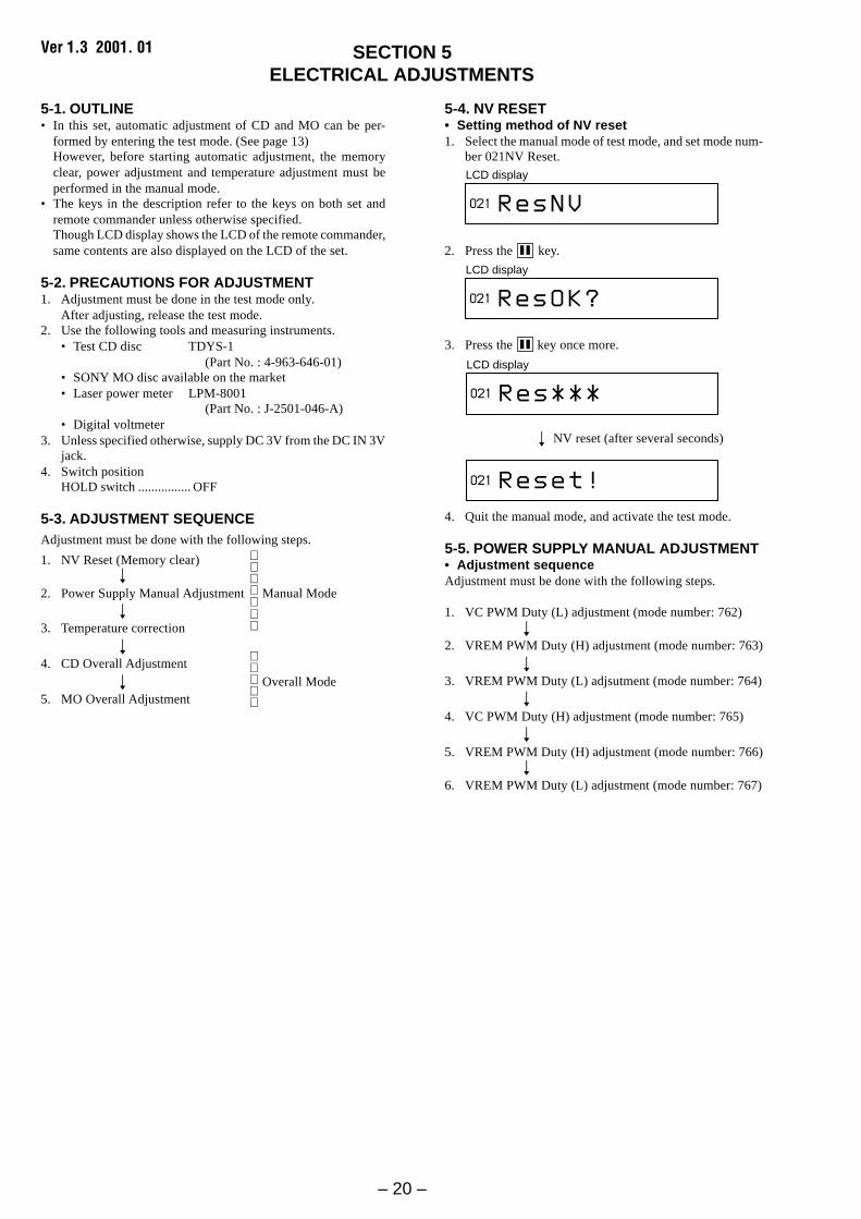
5-4. NV RESET• Setting method of NV reset1. Select the manual mode of test mode, and set mode num-
ber 021NV Reset.
2. Press the X key.
3. Press the X key once more.
r NV reset (after several seconds)
4. Quit the manual mode, and activate the test mode.
5-5. POWER SUPPLY MANUAL ADJUSTMENT• Adjustment sequenceAdjustment must be done with the following steps.
1. VC PWM Duty (L) adjustment (mode number: 762)r
2. VREM PWM Duty (H) adjustment (mode number: 763)r
3. VREM PWM Duty (L) adjsutment (mode number: 764)r
4. VC PWM Duty (H) adjustment (mode number: 765)r
5. VREM PWM Duty (H) adjustment (mode number: 766)r
6. VREM PWM Duty (L) adjustment (mode number: 767)
LCD display
R e s N V021
LCD display
R e s O K ?021
LCD display
R e s * * *021
R e s e t !021
Ver 1.3 2001. 01
– 21 –
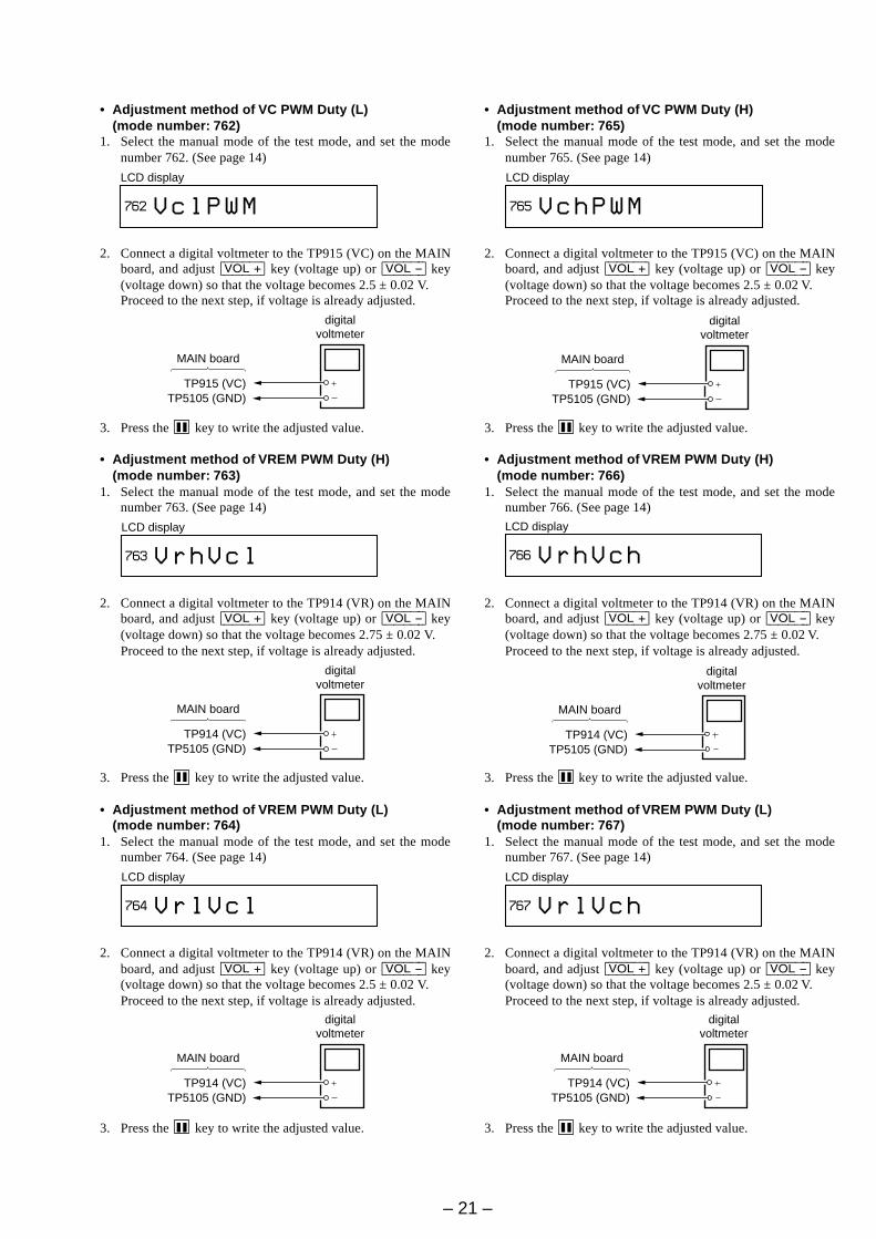
• Adjustment method of VC PWM Duty (L)(mode number: 762)
1. Select the manual mode of the test mode, and set the modenumber 762. (See page 14)
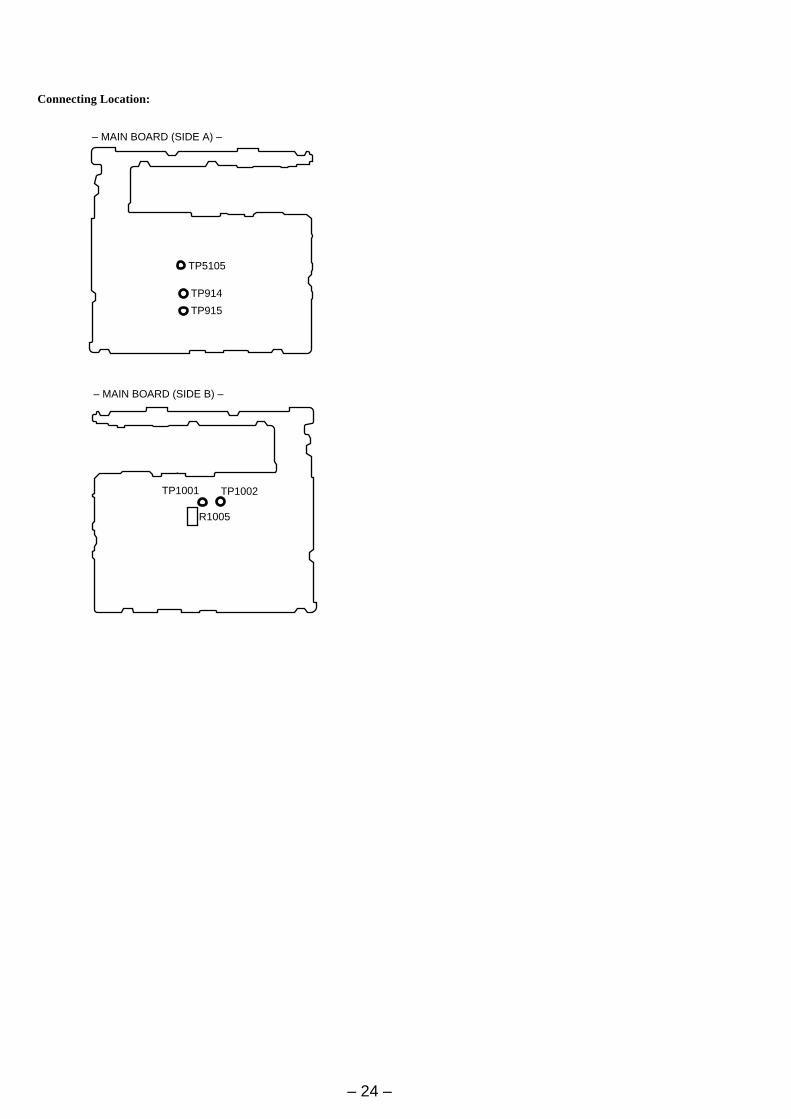
2. Connect a digital voltmeter to the TP915 (VC) on the MAINboard, and adjust [VOL +] key (voltage up) or [VOL --] key(voltage down) so that the voltage becomes 2.5 ± 0.02 V.Proceed to the next step, if voltage is already adjusted.
3. Press the X key to write the adjusted value.
• Adjustment method of VREM PWM Duty (H)(mode number: 763)
1. Select the manual mode of the test mode, and set the modenumber 763. (See page 14)
2. Connect a digital voltmeter to the TP914 (VR) on the MAINboard, and adjust [VOL +] key (voltage up) or [VOL --] key(voltage down) so that the voltage becomes 2.75 ± 0.02 V.Proceed to the next step, if voltage is already adjusted.
3. Press the X key to write the adjusted value.
• Adjustment method of VREM PWM Duty (L)(mode number: 764)
1. Select the manual mode of the test mode, and set the modenumber 764. (See page 14)
2. Connect a digital voltmeter to the TP914 (VR) on the MAINboard, and adjust [VOL +] key (voltage up) or [VOL --] key(voltage down) so that the voltage becomes 2.5 ± 0.02 V.Proceed to the next step, if voltage is already adjusted.
3. Press the X key to write the adjusted value.
V c l P W M762
LCD display
digital voltmeter
MAIN board
TP915 (VC)TP5105 (GND)
V r h V c l763
LCD display
digital voltmeter
MAIN board
TP914 (VC)TP5105 (GND)
V r l V c l764
LCD display
digital voltmeter
MAIN board
TP914 (VC)TP5105 (GND)
• Adjustment method of VC PWM Duty (H)(mode number: 765)
1. Select the manual mode of the test mode, and set the modenumber 765. (See page 14)
2. Connect a digital voltmeter to the TP915 (VC) on the MAINboard, and adjust [VOL +] key (voltage up) or [VOL --] key(voltage down) so that the voltage becomes 2.5 ± 0.02 V.Proceed to the next step, if voltage is already adjusted.
3. Press the X key to write the adjusted value.
• Adjustment method of VREM PWM Duty (H)(mode number: 766)
1. Select the manual mode of the test mode, and set the modenumber 766. (See page 14)
2. Connect a digital voltmeter to the TP914 (VR) on the MAINboard, and adjust [VOL +] key (voltage up) or [VOL --] key(voltage down) so that the voltage becomes 2.75 ± 0.02 V.Proceed to the next step, if voltage is already adjusted.
3. Press the X key to write the adjusted value.
• Adjustment method of VREM PWM Duty (L)(mode number: 767)
1. Select the manual mode of the test mode, and set the modenumber 767. (See page 14)
2. Connect a digital voltmeter to the TP914 (VR) on the MAINboard, and adjust [VOL +] key (voltage up) or [VOL --] key(voltage down) so that the voltage becomes 2.5 ± 0.02 V.Proceed to the next step, if voltage is already adjusted.
3. Press the X key to write the adjusted value.
V c h P W M765
LCD display
digital voltmeter
MAIN board
TP915 (VC)TP5105 (GND)
V r h V c h766
LCD display
digital voltmeter
MAIN board
TP914 (VC)TP5105 (GND)
V r l V c h767
LCD display
digital voltmeter
MAIN board
TP914 (VC)TP5105 (GND)
– 22 –
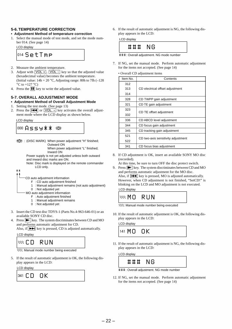
7. If NG, set the manual mode. Perform automatic adjustmentfor the items not accepted. (See page 14)
• Overall CD adjustment items
Item No. Contents
312
313 CD electrical offset adjustment
314
328 CD TWPP gain adjustment
321 CD TE gain adjustment
323CD TE offset adjustment
332
336 CD ABCD level adjustment
344 CD focus gain adjustment
345 CD tracking gain adjustment
521CD two-axis sensitivity adjustment
522
341 CD focus bias adjustment
8. If CD adjustment is OK, insert an available SONY MO disc(recorded).At this time, be sure to turn OFF the disc protect switch.
9. Press N key. The system discriminates between CD and MOand performs automatic adjustment for the MO disc.Also, if . key is pressed, MO is adjusted automatically.However, when CD adjustment is not finished, “SetCD!” isblinking on the LCD and MO adjustment is not executed.
10. If the result of automatic adjustment is OK, the following dis-play appears in the LCD:
11. If the result of automatic adjustment is NG, the following dis-play appears in the LCD:
12. If NG, set the manual mode. Perform automatic adjustmentfor the items not accepted. (See page 14)
LCD display
M O O K141
LCD display
# # # : Overall adjustment. NG mode number
# # # N G
5-6. TEMPERATURE CORRECTION• Adjustment Method of temperature correction1. Select the manual mode of test mode, and set the mode num-
ber 014. (See page 14)
2. Measure the ambient temperature.3. Adjust with [VOL +], [VOL --] key so that the adjusted value
(hexadecimal value) becomes the ambient temperature.(Initial value: 14h = 20 °C, Adjusting range: 80h to 7fh (–128°C to +127 °C)
4. Press the X key to write the adjusted value.
5-7. OVERALL ADJUSTMENT MODE• Adjustment Method of Overall Adjustment Mode1. Setting the test mode. (See page 13)2. Press the . or [VOL --] key activates the overall adjust-
ment mode where the LCD display as shown below.
3. Insert the CD test disc TDYS-1 (Parts No.4-963-646-01) or anavailable SONY CD disc.
4. Press N key. The system discriminates between CD and MOand performs automatic adjustment for CD.Also, if > key is pressed, CD is adjusted automatically.
5. If the result of automatic adjustment is OK, the following dis-play appears in the LCD:
S e t T m p014
LCD display
LCD display
A s s y * *000
: (DISC MARK) When power adjustment “H” finished; Outward ONWhen power adjustment “L” finished; Inward ON
Power supply is not yet adjusted unless both outward and inward disc marks are ON.Note: Disc mark is displayed on the remote commander
LCD only.* *
CD auto adjustment information F : CD auto adjustment finished 1 : Manual adjustment remains (not auto adjustment) 0 : Not adjusted yet MO auto adjustment information F : Auto adjustment finished 1 : Manual adjustment remains 0 : Not adjusted yet
LCD display
C D R U N%%%
%%%: Manual mode number being executed
LCD display
C D O K341
LCD display
# # # : Overall adjustment. NG mode number
# # # N G
LCD display
%%%: Manual mode number being executed
M O R U N%%%
6. If the result of automatic adjustment is NG, the following dis-play appears in the LCD:
– 23 –
13. To clear the data in overall adjustment mode, set the manualmode and change the mode number 021 (Res NV) to reset theNV. (See page 14)
14. When both CD and MO overall adjustments are OK, set themanual mode and clear the clock data.For the microprocessor version 1.20 or later, set the mode num-ber 043 (Resume).Note: In the mode number 043 (Resume), “Res***” display cannot
be seen because of too fast processing.
If microprocessor version 1.20 or later
r Press the X key, historical data clear
Note: In step 10, set the clock data to 99Y11M11D11H11M00S,and in step 14, do not set the clock.
R e s u m e043
LCD display
R e s C l r043
• Overall MO adjustment items
Item No. Contents
112
113MO electrical offset adjustment
114
118
221 Low reflective CD TE gain adjustment
223Low reflective CD TE offset adjustment
232
236 Low reflective CD ABCD level adjustment
244 Low reflective CD focus gain adjustment
245 Low reflective CD tracking gain adjustment
121 MO TE gain adjustment
122 MO TE offset adjustment
134 MO TWPP gain adjustment
131MO x2 speed read TWPP offset adjustment
132
136 MO ABCD level adjustment
144 MO focus gain adjustment
145 MO tracking gain adjustment
434 MO write TWPP gain adjustment
431MO write TWPP offset adjustment
432
436 MO write ABCD level adjustment
445 MO write tracking gain adjustment
411MO x1 speed read TWPP offset adjustment
412
448 32 cluster full recording
141 MO focus bias adjustment
5-8. LASER POWER CHECKConnection :
Check Method :1. Select the manual mode of test mode, and set the laser power
adjusting mode. (mode number 010)2. Press the . key continuously until the optical pick-up
moves to the most inward track.3. Open the cover and set the laser power meter on the objective
lens of the optical pick-up.4. Press the N key, and set the laser MO read adjustment mode.
(mode number 011)5. Check that the laser power meter reading is 0.81 ± 0.08 mW.6. Check that the voltage between TP1001 and TP1002 at this
time is below 44 mV.7. Press the N key, and set the laser CD read adjustment
mode. (mode number 012)8. Check that the laser power meter reading is 0.97 ± 0.10 mW.9. Check that the voltage between TP1001 and TP1002 at this
time is below 44 mV.10. Press the N key, and set the laser MO write adjustment mode.
(mode number 013)11. Check that the laser power meter reading is 4.95 ± 0.50 mW.12. Check that the voltage between TP1001 and TP1002 at this
time is below 80 mV.13. Press the x key.14. Release the test mode.
digital voltmeter
MAIN board
laser power meter
Optical pick-upobjective lens
Between TP1001 and TP1002
– 24 –
Connecting Location:
– MAIN BOARD (SIDE A) –
– MAIN BOARD (SIDE B) –
TP5105
TP914
TP915
TP1001 TP1002
R1005
– 25 – – 26 –
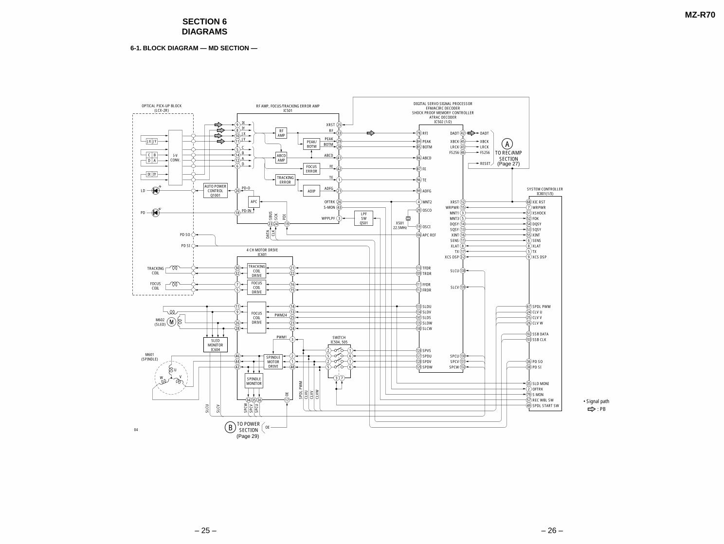
6-1. BLOCK DIAGRAM — MD SECTION —
SECTION 6DIAGRAMS
MZ-R70
04
IXIYJXJY
CBAD
PD-O
PD-IN
RFAMP
ABCDAMP
APC
TRACKINGERROR
FOCUSERROR
PEAK/BOTM
ADIP
RF
PEAKBOTM
FE
ADFG
OFTRKS-MON
WPPLPF
XRST
DADTRFI
PEAKBOTM
ABCD
FE
TE
ADFG
MNT2
OSCO
OSCI
APC REF
TFDRTRDR
FFDRFRDR
SLDUSLDVSLDSSLDWSLCW
SPVSSPDUSPDVSPDW PD SI
SLD MONIOFTRKS MONREC WBL SWSPDL START SW
PD SO
SSB CLKSSB DATA
CLV WCLV VCLV USPDL PWM
XCS DSPTXXLATSENSXINTSQSYDQSYFOKXSHOCKWRPWRXIC RST
TE
ABCD
981011
514126
20
18
23 24 19
25
33
2928
41
42
1
21
2643
3
RF AMP, FOCUS/TRACKING ERROR AMPIC501
I-VCONV.
JX JY
C BD A
IX IY
AUTO POWERCONTROL
Q1001
SLEDMONITOR
IC604
LD
PD
SBUS
SCK
PDI
DATA CLK
TRACKINGCOIL
DRIVE
3032
2122
4 CH MOTOR DRIVEIC601
FOCUSCOIL
DRIVE
LPFSW
Q501
SPINDLEMOTORDRIVE
SPINDLEMONITOR
75
1615
FOCUSCOIL
DRIVE
119
2628
464442
34 35 36 17
1413252324
2
3
148
PWM24
PWM1
M602(SLED)
TRACKINGCOIL
FOCUSCOIL
M601(SPINDLE)
OE
SPDL
PW
MCL
VU
SPCW
SLCV
SLCU
SPCV
SPCU
CLVV
CLVW
TO POWERSECTIONB OE
U
VW
PD SO
PD SI
OPTICAL PICK-UP BLOCK(LCX-2R)
52
25
3 7
61
16
SWITCHIC504, 505
X50122.5MHz
124127128129
106
110109
138
139
130131132
111112
133134141135140
20
4
99
96
87
19
8485
78 42
XBCK 45LRCK 43
FS256
DADT
XBCKLRCKFS256
RESET
46
XRST 12WRPWR 15
MNT1 3MNT3 5DQSY 14SQSY 13XINT 16
SENS 11XLAT 8
TX 17XCS DSP 32
SLCU
SLCV
SPCUSPCV
SPCW
86
DIGITAL SERVO SIGNAL PROCESSOREFM/ACIRC DECODER
SHOCK PROOF MEMORY CONTROLLERATRAC DECODER
IC502 (1/2)
TO REC/AMPSECTION
A
68751525453556859
35
67242526
2795749
SYSTEM CONTROLLERIC801(1/3)
102103
3638
• Signal path : PB
(Page 27)
(Page 29)
MZ-R70
– 27 – – 28 –
6-2. BLOCK DIAGRAM — AUDIO SECTION —
OVER WRITEHEAD DRIVEQ601, 602
SWITCHINGREGULATOR
Q603
EFMLOGIC
A/DCONV.
04
EFM
MOTORDRIVE
F1R1
CLKM603OVER WRITE
HEADUP/DOWNMOTOR
HR601OVERWRITEHEAD
3133
57
1819
35
32
34
OE 24RECDW TP
EFMOSTDO
STDI
BCLKLRCKMCLKXRST
FS4
DW BT
REC +B
23B+SW
BATT +B
22
REC DRIVEIC603
123
113
DIN1 33LIN 2
41LIN 1
44
RIN 240
RIN 143
LOUT 229
ROUT 228
XCS 12PD
KEY-R
47
ADDT
DADT
XBCKLRCK
FS256RESET
41
SWDT 6SCLK 7SRDT 10
DI XPD ADAXCS ADASCLK
DOXCS
4
5
32146
MUTESTB
CDTI15CCLK13CDTO
SWDTSCLK
14
SO0SCK0SI0XCS NV
D/ACONV.
DIGITAL SIGNAL PROCESSOREFM/ACIRC ENCODER
ATRAC ENCODER16M BIT DRAM
IC502 (2/2)
TO PBSECTIONA
BEEP
POWER/LCDSECTION
CTO
POWER/LCDSECTION
D
121311
HD CON130HD CON231
MODE 127MODE 228MODE 329
119
111110
SYSTEM CONTROLLERIC801 (2/3)
3
BEEP 18
19
XHP STBY 23MUTE 117
XOPT CONT 116XJACK DET 114
OPT DET 113XMIC DET 115
RMC DTCK
241
EEPROMIC802
1817
15
22
24
2
23
R-CH
R-CH
RVCC
KEY-RDTCK
R-CH
R-CH HEADPHONE AMPIC303
OPTCONTROL
Q302
R-CH
R-CH
R-CH
VC +B
14 12
9
STBY
MIC AMPIC302
1
J304
2
J302
J303MIC IN
(PLUG IN POWER)
J301LINE IN
(OPTICAL)
A/D, D/A CONVERTERIC301
i
i
• Signal path : REC : PB
(Page 26)
(Page 29) (Page 29)
MZ-R70
– 29 – – 30 –
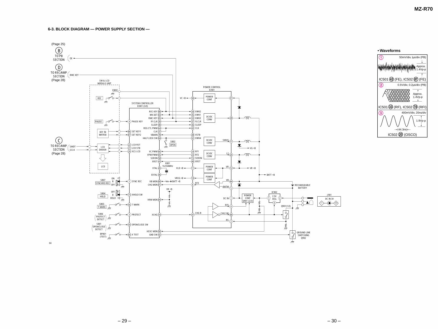
04
TO PBSECTION
BOE
TO REC/AMPSECTION
DRMC KEY
TO REC/AMPSECTION
CSWDTSCLK
REC
SW & LCDMODULE UNIT
PAUSE
SYSTEM CONTROLLERIC801 (3/3)
888385394064377884
66
REC KEY
VC +B
WK DETRMC KEY
FF CLRSLEEP
REG CTL PWMCLK
VBAKNHALF LOCK SW
VC PWM65VPM PWM58SERON43XRST
45XTAL VLD +B
46EXTAL
80VB MON81CHG MON
42GND SW90HI DC MON
59XCHG
89VRM MON
35 XWK133 XWK337 FLCLR36 SLEEP43 CLK
38 VSTB32 XWK4
24 RF123 RF215 SERON40 XRST
RF3
BATT +B
VR +B
VG +B
11 12
44
5
1
34 XWK2
4 PAUSE KEY
86 SET KEY187 SET KEY2
22 LCD RST21 LCD STB20 XCS LCD
1 SYNC REC BATT +B
KEY INMATRIX
LCDDRIVER
X80116.934MHzLCD
ON
OFF
S807SYNCHRO REC
73 XHOLD SW
56 T MARK
OFF
HOLD
S804HOLD
S803T MARK
60 X TESTBP801(TEST)
3 PROTECTS806PROTECTDETECT
50 OPEN/CLOSE SWS801OPEN/CLOSE
DETECT
VR +B
POWERCONT
VREG +B 10
8
CHG B47
POWERCONT
POWERCONT
Q901 (2/2)
2.5VREG
VR
26DC/DCCONV
L2
VB
BATM
4RF5
48CHG SW
2RS
DC IN
S802OPEN
1
5
2
IC902
Q901(1/2)
RECHARGEABLEBATTERY
GROUND LINESWITCHING
Q902
17DC/DCCONV
SWVG
28DC/DCCONV
31POWERCONT
POWER CONTROLIC901
DC IN 3V
J901
30
XWKI
6-3. BLOCK DIAGRAM — POWER SUPPLY SECTION —
(Page 25)
(Page 28)
(Page 28)
1
IC501rs (FE), IC502ij (FE)
2
IC501ed (RF), IC502uk (RFI)
Approx.1.4Vp-p
3
IC502 w; (OSCO)
1.9Vp-p
• Waveforms
44.3ns
400mV/div, 20ns/div
0.5V/div, 0.2µs/div (PB)
50mV/div, lµs/div (PB)
Approx.1.4Vp-p
– 31 – – 32 –
MZ-R70
1
A
B
C
D
E
F
G
H
I
2 3 4 5 6 7 8 9 10 11
TP904
C638
R619
C632
C525
C925
L901
LF90
1
TH90
1
D907
C930
C905
C917
C915
L903
C528
C527
C617
C618
C616
FB50
5
C304
L301
C303
C202
C113
C103
C102
C334
C625C6
23
C624
R525
R636
C640
R526
S802(OPEN)
R815
R811
R834
R835
R808
R806
R840
R805
R803
R802
R801
R614
C600
R814
R812
R938
R928C9
21
R927
R931
R934
R912
R919
R908
R903
R203
R208
R223
C926
R528
C510
R524 R321
TP344
TP315
TP343
TP333
TP332
RB603 RB602
C220
C222
C203
D101 D201
TP331 TP334 TP341
TP335 TP342
L501CN501
L902
TP5112AP5101
AP5102
TP5120
R204
R104
R102
TP347
TP348
D905
TP903
C122
R301
R202
C307
C333
C106
C308 R201
C120
R325
C913
C524
R101
R322
R930
L905
L904
L603Q905
C933C932
C935
C922
TP823
C923
C934
D906
R907
C206
C902
111-677-124-
TP905
TP906
TP311
TP312
TP313
TP314TP316
TP317
TP336TP337
TP346 TP345
TP338
C201 R209R921
R307
R302
C534
R520C536
R522
R838
TP828
AP808
TP5118
AP5119
TP914
TP915
R942
R929
R937
R936
C918C910C929
R923
R924 R913
R612R639
TP601
04 D600
D601
Q603
R611C612
R637L606
C605
C613
C615 C614
C601
C602R613
D602
R809
R813
R807TP816
AP909 AP910
C810
S803T.MARK
OPTICALPICK-UP
TP9001TP801
C535
FB601IC504 IC505
C629
8 51 4
8 51 4 C514
IC601
AP530
TP5105
L601
C621
L604X501
C631
R638
S801(OPEN/CLOSE)
MAIN BOARD (SIDE A)
1
4
8
5
1
5
10
152025
30
3540 45 48
1
10
20
J304(1/2)
J301(1/2)
LINE IN(OPTICAL)
i 1
(LINE OUT)
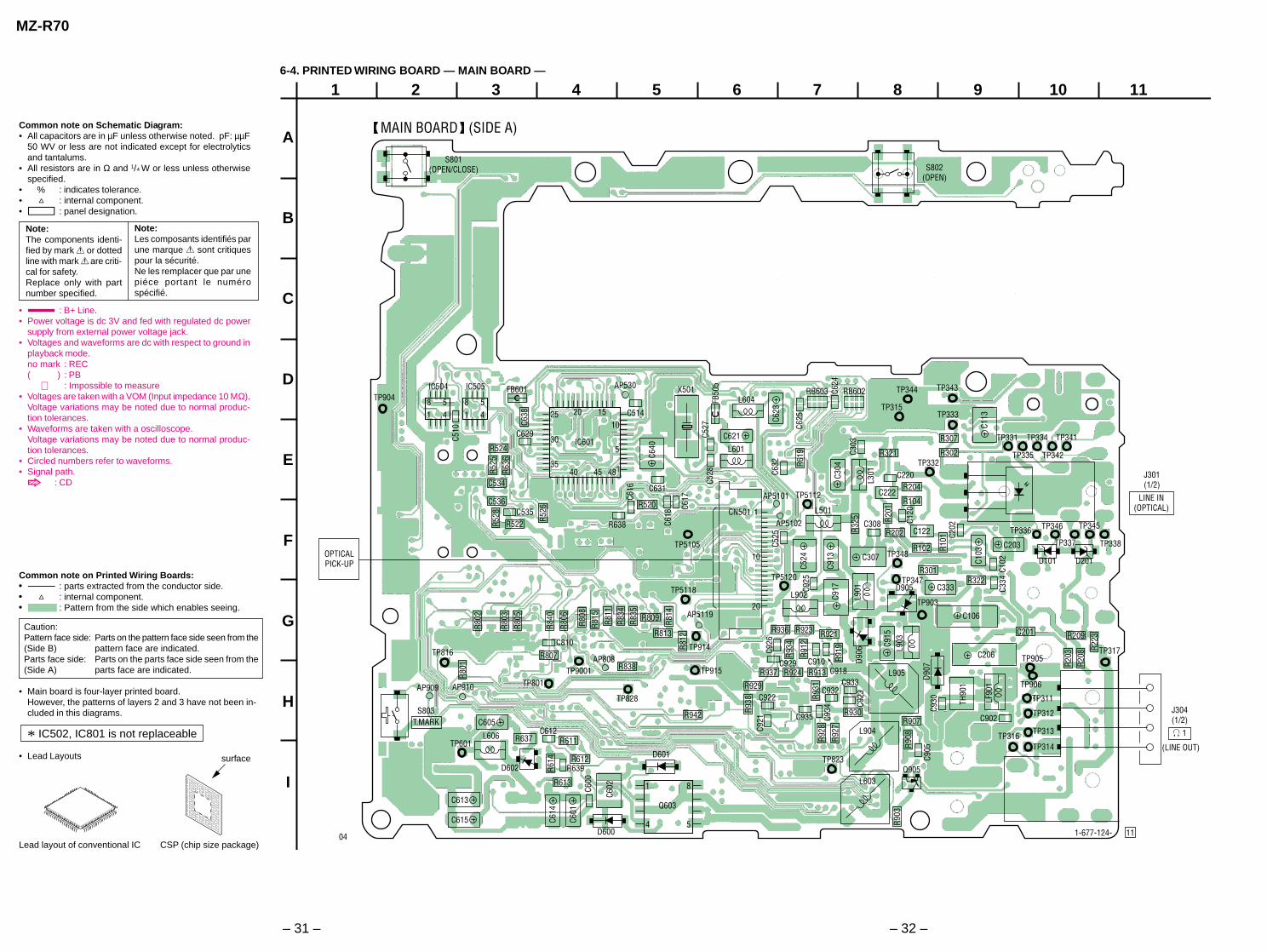
Common note on Printed Wiring Boards:• Y : parts extracted from the conductor side.• f : internal component.• : Pattern from the side which enables seeing.
Caution:Pattern face side: Parts on the pattern face side seen from the(Side B) pattern face are indicated.Parts face side: Parts on the parts face side seen from the(Side A) parts face are indicated.
• Main board is four-layer printed board.However, the patterns of layers 2 and 3 have not been in-cluded in this diagrams.
* IC502, IC801 is not replaceable
• Lead Layouts surface
Lead layout of conventional IC CSP (chip size package)
Common note on Schematic Diagram:• All capacitors are in µF unless otherwise noted. pF: µµF
50 WV or less are not indicated except for electrolyticsand tantalums.
• All resistors are in Ω and 1/4 W or less unless otherwisespecified.
• % : indicates tolerance.• f : internal component.• C : panel designation.
• A : B+ Line.• Power voltage is dc 3V and fed with regulated dc power
supply from external power voltage jack.• Voltages and waveforms are dc with respect to ground in
playback mode.no mark : REC( ) : PB
∗ : Impossible to measure• Voltages are taken with a VOM (Input impedance 10 MΩ).
Voltage variations may be noted due to normal produc-tion tolerances.
• Waveforms are taken with a oscilloscope.Voltage variations may be noted due to normal produc-tion tolerances.
• Circled numbers refer to waveforms.• Signal path.
J : CD
Note:The components identi-fied by mark 0 or dottedline with mark 0 are criti-cal for safety.Replace only with partnumber specified.
Note:Les composants identifiés parune marque 0 sont critiquespour la sécurité.Ne les remplacer que par unepiéce portant le numérospécifié.
6-4. PRINTED WIRING BOARD — MAIN BOARD —
– 33 – – 34 –
MZ-R70
1
A
B
C
D
E
F
G
H
I
J
2345678910111213
R100
5R1
004
R1006
Q1001
IC301
IC501
C210
C108
R211
R112
R118
C216
C118
C116
C320 C3
22C2
12
C332
C111
R319
R317 C2
08
C110
C335
R109
R108
C217
C117
C323 C306
RB302CN602
C213
C112C312
C330
C504C1004
22 1
23 44
C503 C520
C521
C501AP502
C340
R218C318
IC302
8 7
14 1
R122
R222
R123
C337 IC303
C339
R111
C218
C321
C223C123
C211
C331
R212R318
R517
RB601TP1001 TP1002
IC604 IC502
Q501
R519
R518
C502
C505
FB50
1
C530
C513
C506
R536
AP532AP533
AP511AP534
11112
23
4567108139
151614181917
20252421262322282729323130363433147
118116
119120
117114113 112
115
110109 111104108 106104105 103101102 100
144 14635 37 46 47 50 53 56 59 64 6842 45 48 51 55 57 60 63 66 67
111110109114
108
112117
113
116
115
118
119
121120
124123
125122
126127
128
130129
131
133135132134
137138136
139141142
140103100
106104
107105
102101
145
97969288
88 87 86 83 81 78 74 72 69 64 63 60 5890 89 85 84 80 77 75 71 68 65 62 59 5793 92 9196 95 9499 98 97
82 79 76 73 70 67 66 61 55 5652 53 5449 50 5146 47 4843 45 4440 41 4237 36 3934 35 36
32 3326 28 3125 29 30
19 22 2721 2320 24
10 13 1611 14 1712 15 18
742 6 8
1 3 5 9
8582787673
98959189868380
99949390878481
777472
7975
43 44 49 52 54 58 61 62 65 697071
38 4039 41
143
AP529AP525 AP523
AP5103
AP5104AP524
AP508AP504
AP505
AP531AP535
R530R529
C529
R535
C533
R527
C519
C630
R537
R621 C5
26
C619
S807SYNCHRO REC
S804HOLD
C620
C938
C937
C622
AP1001
L502FB503FB502
FB504
BP801
AP519
AP830
AP521
OFF ON
C532
L605
L602
R507
C336
C338
C806 L8
01
C100
1
C507
C517
C515
R506
R842
R100
1
C919
C936
C901
R503
R508
R509
R510
C537
R935
R609 R608
C633
R1010
R1003
R1002
R905
R306C310
C1002
C522
D901
C904
Q301Q901
Q302
R906
C939
FB30
1
R922
C920
R901
R902
C317
04
C319D301
C316
C315
C324
FB303
FB302
FB304
C1243
J901DC IN 3V
4
1
1 14 1 5
5IC902
C311
C224
D302
D902
R103
C301 C1
003
L302
R305
C903
C916
R939 R915
C911
D501
AP5209
AP806C801 AP911
AP807AP907
AP834AP517X801
AP511AP516
AP5210
C610 C611 C609
R505
C511AP509
C516C512
C509AP506
AP501 AP510
AP83
3
AP802AP912
AP515 AP518AP832
AP520AP512
AP908
AP801
AP80
4AP
803
AP507
AP805C508
C807
R944R914
R904
R911
R916
CN601 Q601 Q602
IC802
IC603
IC801
CN801
R940
C906
Q906
R932
Q902
41
58
S
D903
C101
R941R502
C531
1
1 7
2 8
2 8
1 7
4
8
5
1
1
5
10
1315202425
30
3540 45 48
7 12
24 19
6
18
13
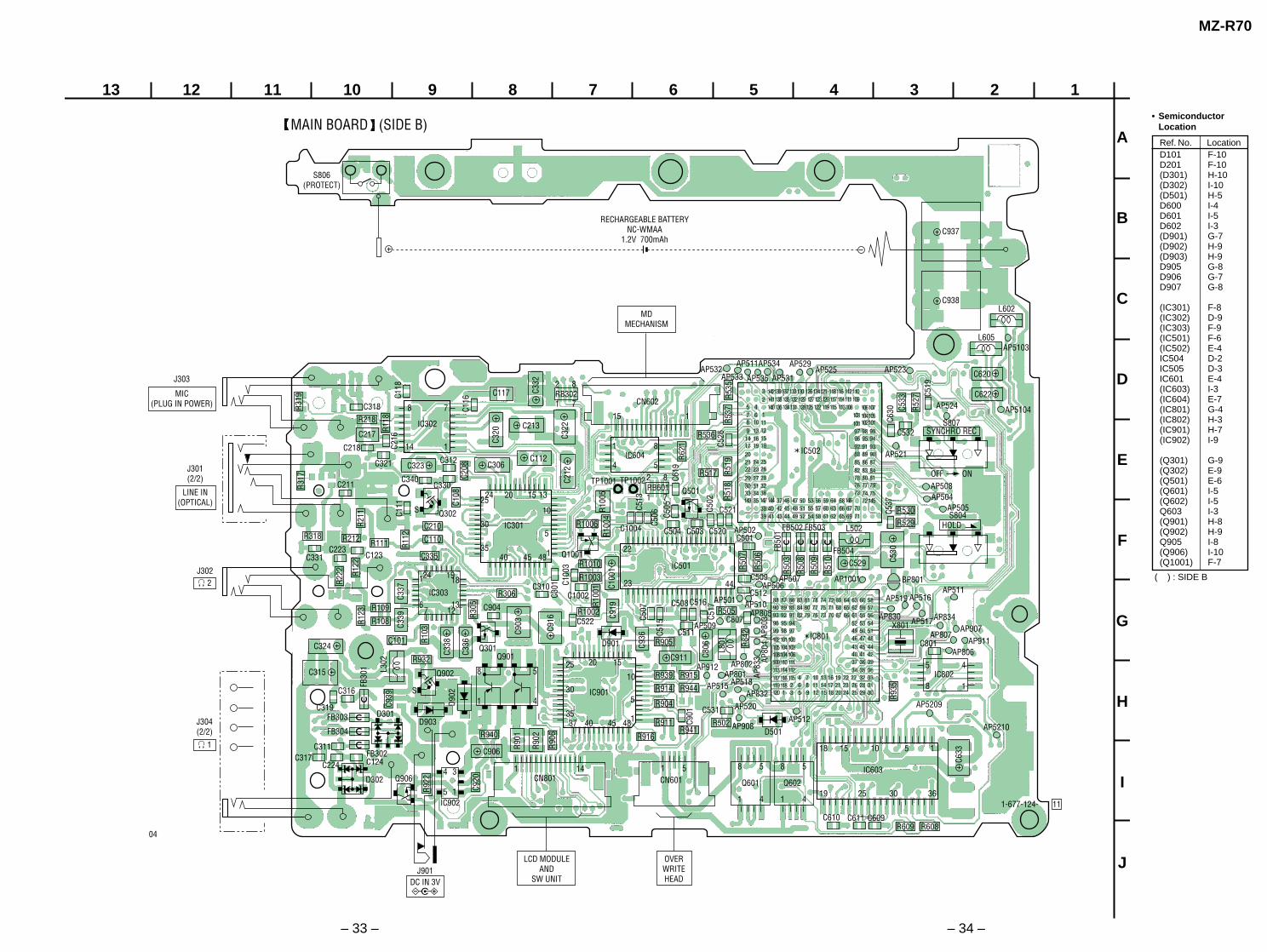
MAIN BOARD (SIDE B)
111-677-124-
8 1
5 4
S806(PROTECT)
5
1025 1520
1
30
3537 40 45 48
IC901
!
1 4 1 4
8 5 8 5
118 51015
3619 3025
RECHARGEABLE BATTERYNC-WMAA
1.2V 700mAh
MDMECHANISM
LCD MODULEAND
SW UNIT
OVERWRITEHEAD
115
J304(2/2)
i 1
J302
J301(2/2)
LINE IN(OPTICAL)
i 2
J303
MIC(PLUG IN POWER)
S
D101 F-10D201 F-10(D301) H-10(D302) I-10(D501) H-5D600 I-4D601 I-5D602 I-3(D901) G-7(D902) H-9(D903) H-9D905 G-8D906 G-7D907 G-8
(IC301) F-8(IC302) D-9(IC303) F-9(IC501) F-6(IC502) E-4IC504 D-2IC505 D-3IC601 E-4(IC603) I-3(IC604) E-7(IC801) G-4(IC802) H-3(IC901) H-7(IC902) I-9
(Q301) G-9(Q302) E-9(Q501) E-6(Q601) I-5(Q602) I-5Q603 I-3(Q901) H-8(Q902) H-9Q905 I-8(Q906) I-10(Q1001) F-7
• SemiconductorLocation
Ref. No. Location
( ) : SIDE B
– 35 – – 36 –
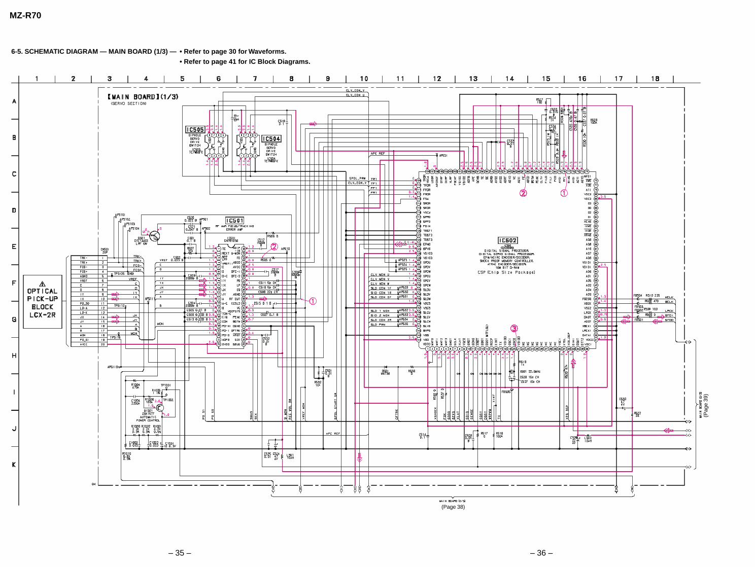
6-5. SCHEMATIC DIAGRAM — MAIN BOARD (1/3) — • Refer to page 30 for Waveforms.
• Refer to page 41 for IC Block Diagrams.
MZ-R70
(Page 38)
(Pag
e 39
)
– 37 – – 38 –
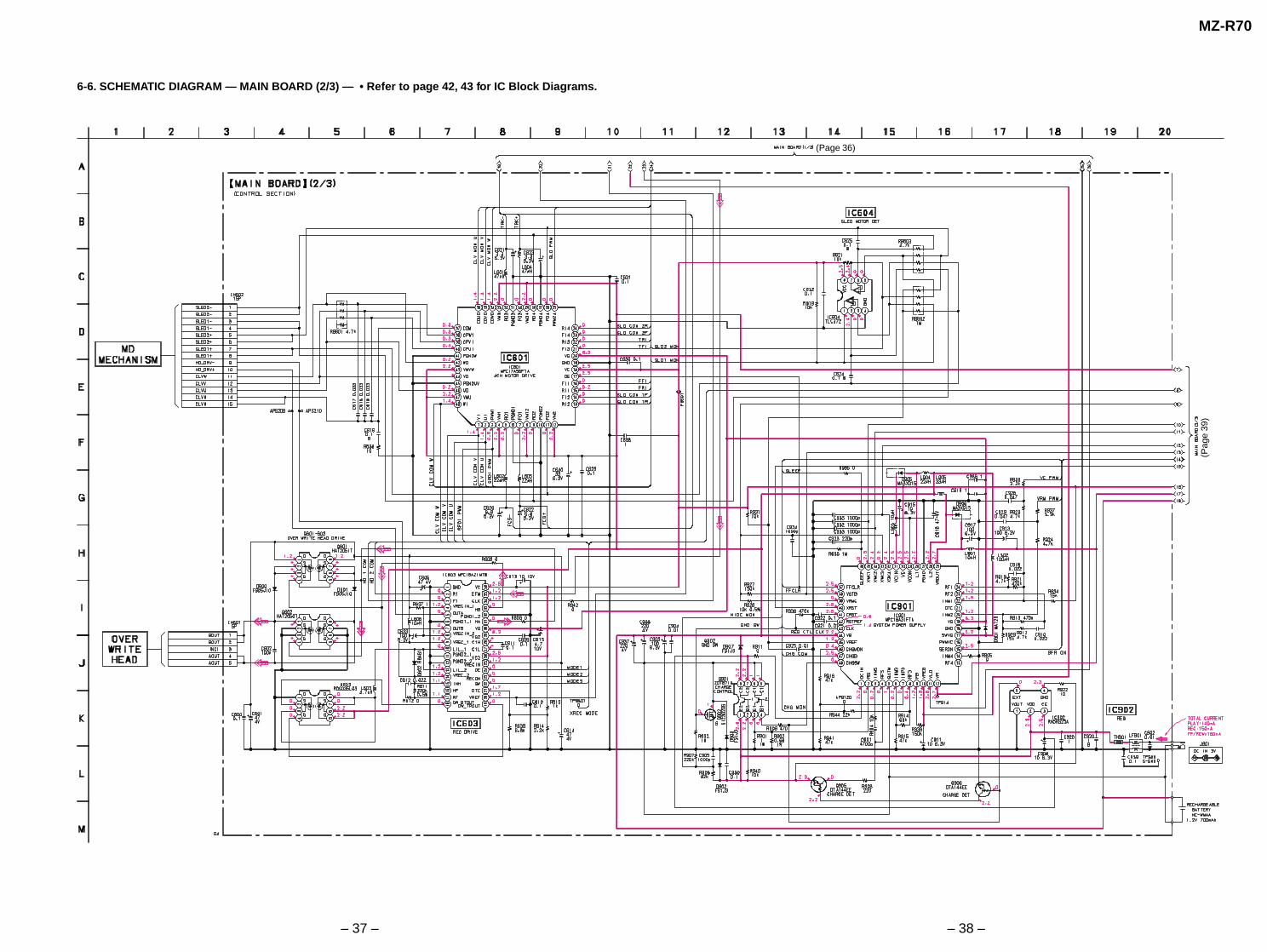
MZ-R70
6-6. SCHEMATIC DIAGRAM — MAIN BOARD (2/3) — • Refer to page 42, 43 for IC Block Diagrams.
(Page 36)
(Pag
e 39
)
– 39 – – 40 –
MZ-R70
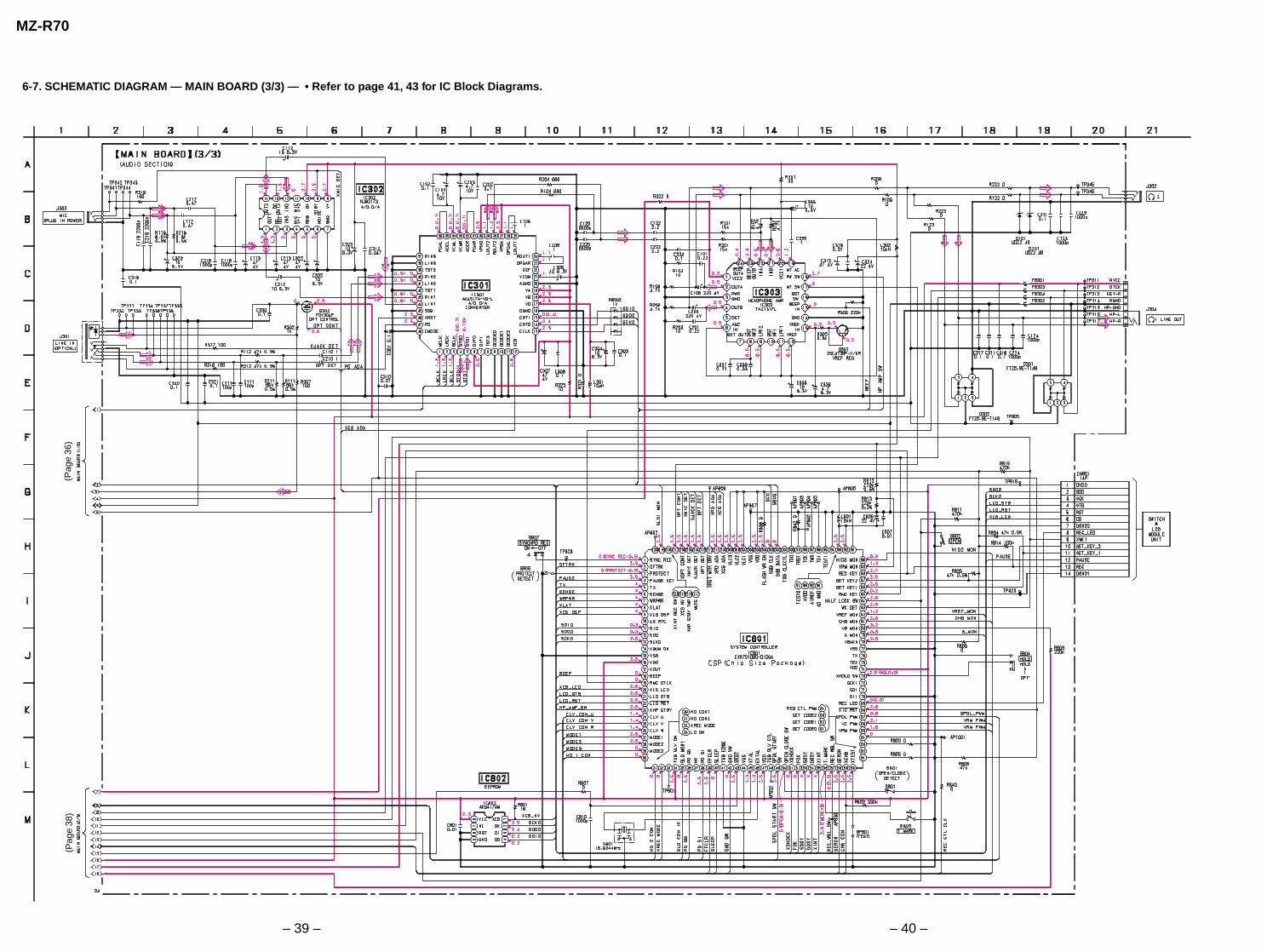
6-7. SCHEMATIC DIAGRAM — MAIN BOARD (3/3) — • Refer to page 41, 43 for IC Block Diagrams.
(Pag
e 36
)(P
age
38)
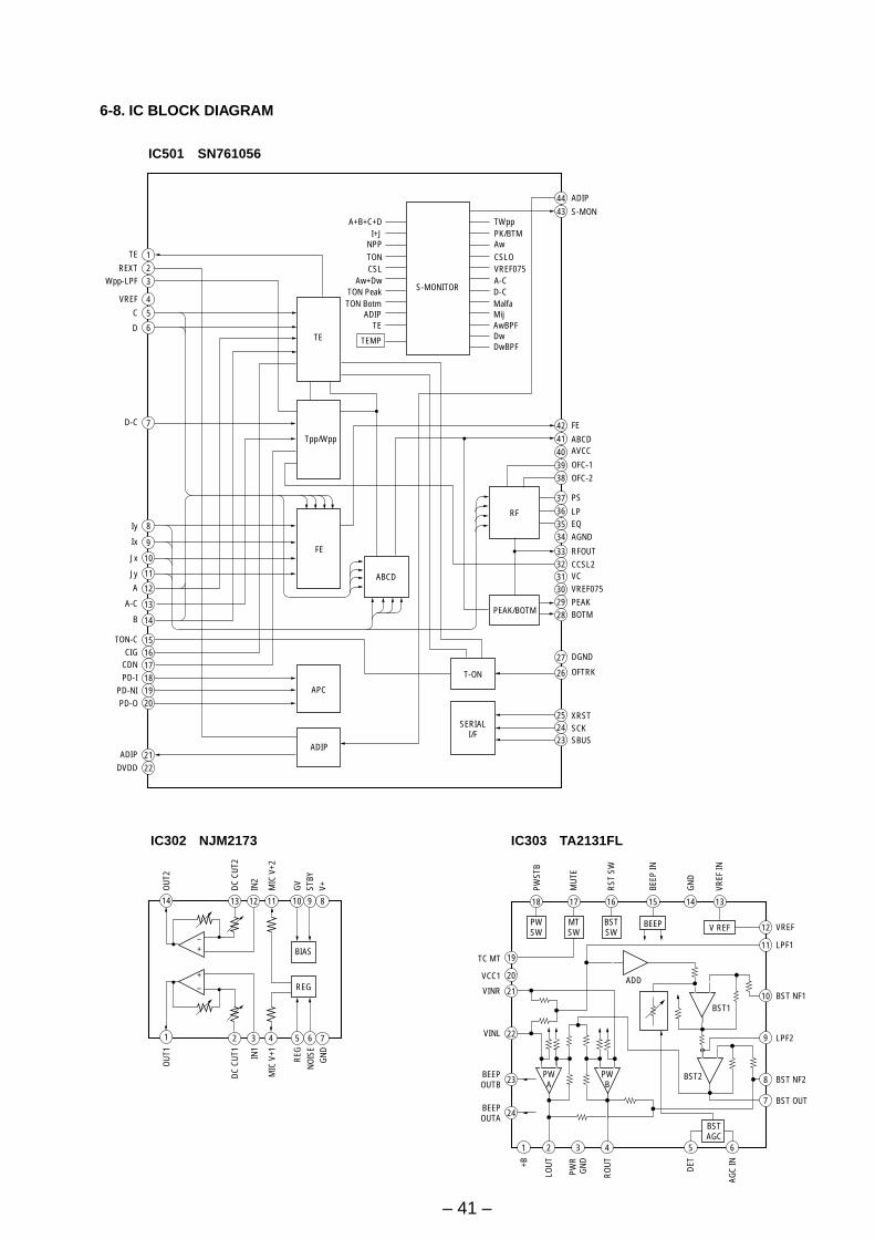
– 41 –
IC501 SN761056
IC303 TA2131FLIC302 NJM2173
6-8. IC BLOCK DIAGRAM
1TE
REXTWpp-LPF
VREF
C
D
D-C
Iy
Ix
Jx
Jy
A
A-C
B
ADIP
FE
ABCDAVCC
OFC-1OFC-2
PS
LPEQAGND
RFOUTCCSL2VC
XRSTSCKSBUS
VREF075PEAKBOTM
DGND
OFTRK
S-MON
TON-CCIG
CDN
ADIPDVDD
PD-IPD-NIPD-O
4344
TWppPK/BTMAwCSLOVREF075A-CD-CMalfaMijAwBPFDwDwBPF
42
38
37363534
31302928
27
26
252423
39
4140
23
4
5
6
7
8
9
10
11
12
13
14
151617181920
2122
A+B+C+DI+J
NPPTONCSL
Aw+DwTON PeakTON Botm
ADIPTE
TEMP
3332
S-MONITOR
TE
RF
FE
APC
ADIP
T-ON
SERIALI/F
PEAK/BOTM
ABCD
Tpp/Wpp
1
14
OUT1
2
DC C
UT1
3
IN1
4
MIC
V+1
REG
NOIS
EGN
D
13
DC C
UT2
OUT2
12
IN2
11
MIC
V+2
10
GV
9 8
75 6
STBY
V+
+–
+– REG
BIAS
V REFMTSW
BSTSW
BEEP
19
20
21
22
23
24
18 17 16 15 14 13
PWSW 12
11
10
8
7
BST1
9
BST2
654321
BSTAGC
PWB
PWA
ADD
TC MT
VCC1
VINR
VINL
BEEPOUTB
BEEPOUTA
+B
LOUT
PWR
GND
ROUT DE
T
AGC
IN
BST OUT
BST NF2
LPF2
BST NF1
LPF1
VREF
VREF
IN
GND
BEEP
IN
RST
SW
MUT
E
PWST
B
– 42 –
1234
5
6
VCEFMCLK
HB
PGND1 2
HA
VGVG2
C1H
C1L
VC2
VRECINOERECON
SW(2.5/1.3V)DTCVREFDW TPOUT
GNDR1F1
VRECIN 1
OUTA
PGND1 1
OUTB
VRECIN 2
VREC 1
LIL 1
PGND2 1PGND2 2
LIL 2VREC 2
INMINP
RFDW BTOUT
7
8
9
10
11121314
1516
CONTROLLOGIC
PREDRIVER
STEPUP/DOWN
PREDRIVER
PWM
EFMPRE
DRIVER
CHARGEPUMPPRE
DRIVER
LEVELDET
33
3130
28
27
26
252423
29
32
34
3635
SYSTEMCONTROL
SAW
1718
22212019
+-
36
24
1615
38
39
40
35 34 33 32 31 30 29 28 27 26 25
4 5 6 7 9 10 11 12
37
44
46
47
414243
81
VI
RO1
PGND
1
FO1
VM12
RO2
PGND
2
FO2
RI2
FI2
RI1FI1
OE
VC
GND
VG
FI3RI3FI4
RI4
PWM
24
FO4
VM4
PGND
4
RO4
VM34
FO3
PGND
3
RO3
VM3
COM
CPWI
CPVI
PGNDWWO
VMVW
VO
PGNDUVUO
WI
VMU
CPUI
COW
OCO
VOCO
UO
VC
VC
VC
VG
VC
VG
VC
VC
VG
VC
VCVG
VC
VCVG
VC
VCVG
VM2
VM1UI
PWM
1
2 3
48
45
232221
2019
1718
14
13
BIAS
PRE DRIVER
HI-BRIDGECONTROL
PRE DRIVER
PRE DRIVER
HI-BRIDGECONTROL
3 PHASECONTROL
PRE DRIVER
HI-BRIDGECONTROL
HI-BRIDGECONTROL
PRE DRIVER
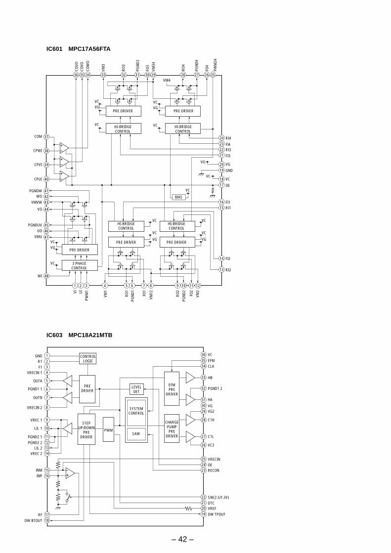
IC601 MPC17A56FTA
IC603 MPC18A21MTB
– 43 –
CLOCKDIVIDER
CONTROLREGISTER
I/F
AUDIOI/F
CONTROLLERHPF
IPGALMCLK
CMOD
ECC
LK(S
SI)
CDTI
(SSO
)CD
TO
DGND VD VB VA
AGND
VCOM DZ
FOP
GAR
ROUT
1
PD RST
SSB
LIN1
RIN1
TST1
LIN2
RIN2
TST2
LIN3
RIN3
LRCKBCLKSDTOSDTIDIFODIFI
TST3
DCODE0DCODE1DCODE2CS(SCK)
ADCLVCMCVCMRADCR
IPGARVRAD
LOUT2
ROUT2VRDAOPGALLOUT1
ADO
DACDBBDPGA
1
48
36
333435
32
3130
29
28272625
3839404142434445 3747 46
234567
9101112
151413 16 24232217 18 19 20 21
8
37FFCLR
VSTL
VRMC
XRST
CRSTRSTREF
CLK
CHGSW
DCIN
INM
3
RS
INM
5
RF5
BATM
INP3 RF
3 FB
VREG VLD VR
RF4
INM4SERON
PWMVC
SWVGGNDVG
DTCINM1
RF2
RF1
INM2
VB
SLEE
P
VC
VC
VC
RF2 RF2
XRST
FFCLR
VC
VB VC
VG VG
VC
VC
VR
XWK1
XWK2
XWK3
XWK4
VCIN
VC L1 PGND
L2 VROU
T
VCON
VC
DCIN
VB
VREG
RF4
DCIN
DCIN
CHGMON
CHGB
VREF
36 35 34 33 32 31 30 29 28 27 26 25
24
23
222120
191817
161514
13
38
39
40
4142
43
4445
46
47
48
1 2 3 4 5 6 7 8 9 10 11 12
STEP-UPDC/DC
CONVERTER
SAW
OSC2
SYSTEMCONTROL
STEP-UPPRE DRIVER
STEP-UPPRE DRIVER
PWM PWM
BANDGAPREFERENCE
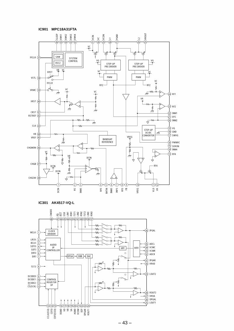
IC901 MPC18A31FTA
IC301 AK4517-VQ-L
– 44 –
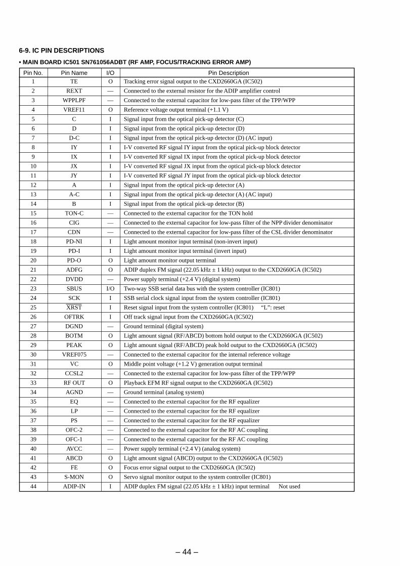
Pin No. Pin Name I/O Pin Description1 TE O Tracking error signal output to the CXD2660GA (IC502)
2 REXT — Connected to the external resistor for the ADIP amplifier control
3 WPPLPF — Connected to the external capacitor for low-pass filter of the TPP/WPP
4 VREF11 O Reference voltage output terminal (+1.1 V)
5 C I Signal input from the optical pick-up detector (C)
6 D I Signal input from the optical pick-up detector (D)
7 D-C I Signal input from the optical pick-up detector (D) (AC input)
8 IY I I-V converted RF signal IY input from the optical pick-up block detector
9 IX I I-V converted RF signal IX input from the optical pick-up block detector
10 JX I I-V converted RF signal JX input from the optical pick-up block detector
11 JY I I-V converted RF signal JY input from the optical pick-up block detector
12 A I Signal input from the optical pick-up detector (A)
13 A-C I Signal input from the optical pick-up detector (A) (AC input)
14 B I Signal input from the optical pick-up detector (B)
15 TON-C — Connected to the external capacitor for the TON hold
16 CIG — Connected to the external capacitor for low-pass filter of the NPP divider denominator
17 CDN — Connected to the external capacitor for low-pass filter of the CSL divider denominator
18 PD-NI I Light amount monitor input terminal (non-invert input)
19 PD-I I Light amount monitor input terminal (invert input)
20 PD-O O Light amount monitor output terminal
21 ADFG O ADIP duplex FM signal (22.05 kHz ± 1 kHz) output to the CXD2660GA (IC502)
22 DVDD — Power supply terminal (+2.4 V) (digital system)
23 SBUS I/O Two-way SSB serial data bus with the system controller (IC801)
24 SCK I SSB serial clock signal input from the system controller (IC801)
25 XRST I Reset signal input from the system controller (IC801) “L”: reset
26 OFTRK I Off track signal input from the CXD2660GA (IC502)
27 DGND — Ground terminal (digital system)
28 BOTM O Light amount signal (RF/ABCD) bottom hold output to the CXD2660GA (IC502)
29 PEAK O Light amount signal (RF/ABCD) peak hold output to the CXD2660GA (IC502)
30 VREF075 — Connected to the external capacitor for the internal reference voltage
31 VC O Middle point voltage (+1.2 V) generation output terminal
32 CCSL2 — Connected to the external capacitor for low-pass filter of the TPP/WPP
33 RF OUT O Playback EFM RF signal output to the CXD2660GA (IC502)
34 AGND — Ground terminal (analog system)
35 EQ — Connected to the external capacitor for the RF equalizer
36 LP — Connected to the external capacitor for the RF equalizer
37 PS — Connected to the external capacitor for the RF equalizer
38 OFC-2 — Connected to the external capacitor for the RF AC coupling
39 OFC-1 — Connected to the external capacitor for the RF AC coupling
40 AVCC — Power supply terminal (+2.4 V) (analog system)
41 ABCD O Light amount signal (ABCD) output to the CXD2660GA (IC502)
42 FE O Focus error signal output to the CXD2660GA (IC502)
43 S-MON O Servo signal monitor output to the system controller (IC801)
44 ADIP-IN I ADIP duplex FM signal (22.05 kHz ± 1 kHz) input terminal Not used
6-9. IC PIN DESCRIPTIONS
• MAIN BOARD IC501 SN761056ADBT (RF AMP, FOCUS/TRACKING ERROR AMP)
– 45 –
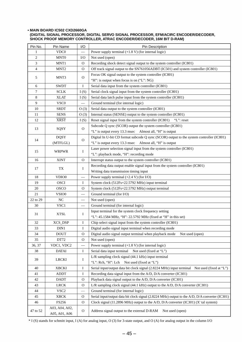
Pin No. Pin Name I/O Pin Description1 VDC0 — Power supply terminal (+1.8 V) (for internal logic)
2 MNT0 I/O Not used (open)
3 MNT1 O Recording shock detect signal output to the system controller (IC801)
4 MNT2 O Off track signal output to the SN761056ADBT (IC501) and system controller (IC801)
5 MNT3 OFocus OK signal output to the system controller (IC801)
“H”: is output when focus is on (“L”: NG)
6 SWDT I Serial data input from the system controller (IC801)
7 SCLK I (S) Serial clock signal input from the system controller (IC801)
8 XLAT I (S) Serial data latch pulse input from the system controller (IC801)
9 VSC0 — Ground terminal (for internal logic)
10 SRDT O (3) Serial data output to the system controller (IC801)
11 SENS O (3) Internal status (SENSE) output to the system controller (IC801)
12 XRST I (S) Reset signal input from the system controller (IC801) “L”: reset
13 SQSY OSubcode Q sync (SCOR) output the system controller (IC801)
“L” is output every 13.3 msec Almost all, “H” is output
14DQSY
ODigital In U-bit CD format subcode Q sync (SCOR) output to the system controller (IC801)
(MTFLGL) “L” is output every 13.3 msec Almost all, “H” is output
15 WRPWR ILaser power selection signal input from the system controller (IC801)
“L”: playback mode, “H”: recording mode
16 XINT O Interrupt status output to the system controller (IC801)
17 TX IRecording data output enable signal input from the system controller (IC801)
Writing data transmission timing input
18 VDIO0 — Power supply terminal (+2.4 V) (for I/O)
19 OSCI I System clock (512Fs=22.5792 MHz) input terminal
20 OSCO O System clock (512Fs=22.5792 MHz) output terminal
21 VSIO0 — Ground terminal (for I/O)
22 to 29 NC — Not used (open)
30 VSC1 — Ground terminal (for internal logic)
31 XTSL IInput terminal for the system clock frequency setting
“L”: 45.1584 MHz, “H”: 22.5792 MHz (fixed at “H” in this set)
32 XCS_DSP I Chip select signal input from the system controller (IC801)
33 DIN1 I Digital audio signal input terminal when recording mode
34 DOUT O Digital audio signal output terminal when playback mode Not used (open)
35 DT72 O Not used (open)
36, 37 VDC1, VDC2 — Power supply terminal (+1.8 V) (for internal logic)
38 DATAI I Serial data input terminal Not used (fixed at “L”)
39 LRCKI IL/R sampling clock signal (44.1 kHz) input terminal
“L”: Rch, “H”: Lch Not used (fixed at “L”)
40 XBCKI I Serial input/output data bit clock signal (2.8224 MHz) input terminal Not used (fixed at “L”)
41 ADDT I Recording data signal input from the A/D, D/A converter (IC301)
42 DADT O Playback data signal output to the A/D, D/A converter (IC301)
43 LRCK O L/R sampling clock signal (44.1 kHz) output to the A/D, D/A converter (IC301)
44 VSC2 — Ground terminal (for internal logic)
45 XBCK O Serial input/output data bit clock signal (2.8224 MHz) output to the A/D, D/A converter (IC301)
46 FS256 O Clock signal (11.2896 MHz) output to the A/D, D/A converter (IC301) (X' tal system)
47 to 52A03, A04, A02,
O Address signal output to the external D-RAM Not used (open)A05, A01, A06
• MAIN BOARD IC502 CXD2660GA(DIGITAL SIGNAL PROCESSOR, DIGITAL SERVO SIGNAL PROCESSOR, EFM/ACIRC ENCODER/DECODER,SHOCK PROOF MEMORY CONTROLLER, ATRAC ENCODER/DECODER, 16M BIT D-RAM)
* I (S) stands for schmitt input, I (A) for analog input, O (3) for 3-state output, and O (A) for analog output in the column I/O
– 46 –
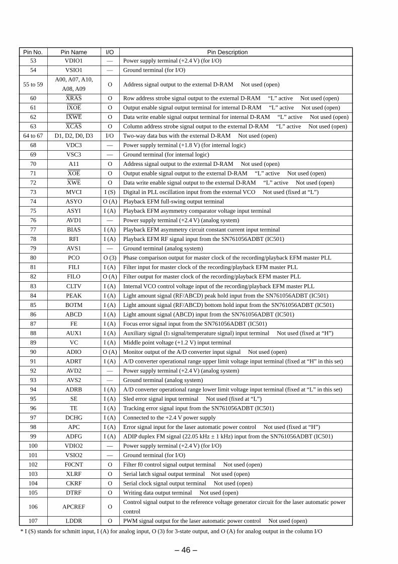
Pin No. Pin Name I/O Pin Description53 VDIO1 — Power supply terminal (+2.4 V) (for I/O)
54 VSIO1 — Ground terminal (for I/O)
55 to 59A00, A07, A10,
O Address signal output to the external D-RAM Not used (open)A08, A09
60 XRAS O Row address strobe signal output to the external D-RAM “L” active Not used (open)
61 IXOE O Output enable signal output terminal for internal D-RAM “L” active Not used (open)
62 IXWE O Data write enable signal output terminal for internal D-RAM “L” active Not used (open)
63 XCAS O Column address strobe signal output to the external D-RAM “L” active Not used (open)
64 to 67 D1, D2, D0, D3 I/O Two-way data bus with the external D-RAM Not used (open)
68 VDC3 — Power supply terminal (+1.8 V) (for internal logic)
69 VSC3 — Ground terminal (for internal logic)
70 A11 O Address signal output to the external D-RAM Not used (open)
71 XOE O Output enable signal output to the external D-RAM “L” active Not used (open)
72 XWE O Data write enable signal output to the external D-RAM “L” active Not used (open)
73 MVCI I (S) Digital in PLL oscillation input from the external VCO Not used (fixed at “L”)
74 ASYO O (A) Playback EFM full-swing output terminal
75 ASYI I (A) Playback EFM asymmetry comparator voltage input terminal
76 AVD1 — Power supply terminal (+2.4 V) (analog system)
77 BIAS I (A) Playback EFM asymmetry circuit constant current input terminal
78 RFI I (A) Playback EFM RF signal input from the SN761056ADBT (IC501)
79 AVS1 — Ground terminal (analog system)
80 PCO O (3) Phase comparison output for master clock of the recording/playback EFM master PLL
81 FILI I (A) Filter input for master clock of the recording/playback EFM master PLL
82 FILO O (A) Filter output for master clock of the recording/playback EFM master PLL
83 CLTV I (A) Internal VCO control voltage input of the recording/playback EFM master PLL
84 PEAK I (A) Light amount signal (RF/ABCD) peak hold input from the SN761056ADBT (IC501)
85 BOTM I (A) Light amount signal (RF/ABCD) bottom hold input from the SN761056ADBT (IC501)
86 ABCD I (A) Light amount signal (ABCD) input from the SN761056ADBT (IC501)
87 FE I (A) Focus error signal input from the SN761056ADBT (IC501)
88 AUX1 I (A) Auxiliary signal (I3 signal/temperature signal) input terminal Not used (fixed at “H”)
89 VC I (A) Middle point voltage (+1.2 V) input terminal
90 ADIO O (A) Monitor output of the A/D converter input signal Not used (open)
91 ADRT I (A) A/D converter operational range upper limit voltage input terminal (fixed at “H” in this set)
92 AVD2 — Power supply terminal (+2.4 V) (analog system)
93 AVS2 — Ground terminal (analog system)
94 ADRB I (A) A/D converter operational range lower limit voltage input terminal (fixed at “L” in this set)
95 SE I (A) Sled error signal input terminal Not used (fixed at “L”)
96 TE I (A) Tracking error signal input from the SN761056ADBT (IC501)
97 DCHG I (A) Connected to the +2.4 V power supply
98 APC I (A) Error signal input for the laser automatic power control Not used (fixed at “H”)
99 ADFG I (A) ADIP duplex FM signal (22.05 kHz ± 1 kHz) input from the SN761056ADBT (IC501)
100 VDIO2 — Power supply terminal (+2.4 V) (for I/O)
101 VSIO2 — Ground terminal (for I/O)
102 F0CNT O Filter f0 control signal output terminal Not used (open)
103 XLRF O Serial latch signal output terminal Not used (open)
104 CKRF O Serial clock signal output terminal Not used (open)
105 DTRF O Writing data output terminal Not used (open)
106 APCREF OControl signal output to the reference voltage generator circuit for the laser automatic power
control
107 LDDR O PWM signal output for the laser automatic power control Not used (open)
* I (S) stands for schmitt input, I (A) for analog input, O (3) for 3-state output, and O (A) for analog output in the column I/O
– 47 –
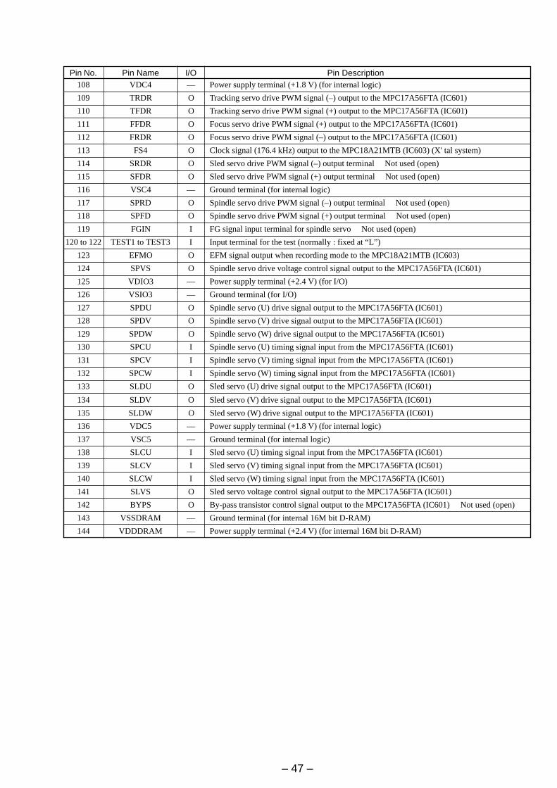
Pin No. Pin Name I/O Pin Description108 VDC4 — Power supply terminal (+1.8 V) (for internal logic)
109 TRDR O Tracking servo drive PWM signal (–) output to the MPC17A56FTA (IC601)
110 TFDR O Tracking servo drive PWM signal (+) output to the MPC17A56FTA (IC601)
111 FFDR O Focus servo drive PWM signal (+) output to the MPC17A56FTA (IC601)
112 FRDR O Focus servo drive PWM signal (–) output to the MPC17A56FTA (IC601)
113 FS4 O Clock signal (176.4 kHz) output to the MPC18A21MTB (IC603) (X' tal system)
114 SRDR O Sled servo drive PWM signal (–) output terminal Not used (open)
115 SFDR O Sled servo drive PWM signal (+) output terminal Not used (open)
116 VSC4 — Ground terminal (for internal logic)
117 SPRD O Spindle servo drive PWM signal (–) output terminal Not used (open)
118 SPFD O Spindle servo drive PWM signal (+) output terminal Not used (open)
119 FGIN I FG signal input terminal for spindle servo Not used (open)
120 to 122 TEST1 to TEST3 I Input terminal for the test (normally : fixed at “L”)
123 EFMO O EFM signal output when recording mode to the MPC18A21MTB (IC603)
124 SPVS O Spindle servo drive voltage control signal output to the MPC17A56FTA (IC601)
125 VDIO3 — Power supply terminal (+2.4 V) (for I/O)
126 VSIO3 — Ground terminal (for I/O)
127 SPDU O Spindle servo (U) drive signal output to the MPC17A56FTA (IC601)
128 SPDV O Spindle servo (V) drive signal output to the MPC17A56FTA (IC601)
129 SPDW O Spindle servo (W) drive signal output to the MPC17A56FTA (IC601)
130 SPCU I Spindle servo (U) timing signal input from the MPC17A56FTA (IC601)
131 SPCV I Spindle servo (V) timing signal input from the MPC17A56FTA (IC601)
132 SPCW I Spindle servo (W) timing signal input from the MPC17A56FTA (IC601)
133 SLDU O Sled servo (U) drive signal output to the MPC17A56FTA (IC601)
134 SLDV O Sled servo (V) drive signal output to the MPC17A56FTA (IC601)
135 SLDW O Sled servo (W) drive signal output to the MPC17A56FTA (IC601)
136 VDC5 — Power supply terminal (+1.8 V) (for internal logic)
137 VSC5 — Ground terminal (for internal logic)
138 SLCU I Sled servo (U) timing signal input from the MPC17A56FTA (IC601)
139 SLCV I Sled servo (V) timing signal input from the MPC17A56FTA (IC601)
140 SLCW I Sled servo (W) timing signal input from the MPC17A56FTA (IC601)
141 SLVS O Sled servo voltage control signal output to the MPC17A56FTA (IC601)
142 BYPS O By-pass transistor control signal output to the MPC17A56FTA (IC601) Not used (open)
143 VSSDRAM — Ground terminal (for internal 16M bit D-RAM)
144 VDDDRAM — Power supply terminal (+2.4 V) (for internal 16M bit D-RAM)
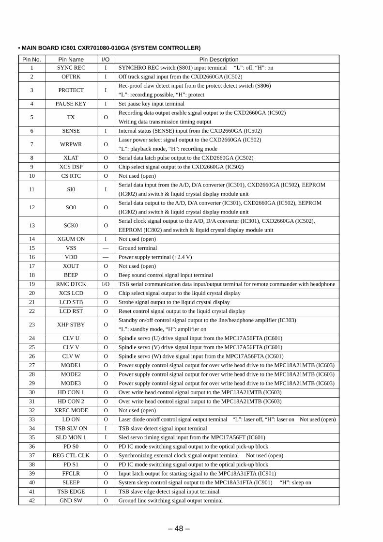
– 48 –
Pin No. Pin Name I/O Pin Description1 SYNC REC I SYNCHRO REC switch (S801) input terminal “L”: off, “H”: on
2 OFTRK I Off track signal input from the CXD2660GA (IC502)
3 PROTECT IRec-proof claw detect input from the protect detect switch (S806)
“L”: recording possible, “H”: protect
4 PAUSE KEY I Set pause key input terminal
5 TX ORecording data output enable signal output to the CXD2660GA (IC502)
Writing data transmission timing output
6 SENSE I Internal status (SENSE) input from the CXD2660GA (IC502)
7 WRPWR OLaser power select signal output to the CXD2660GA (IC502)
“L”: playback mode, “H”: recording mode
8 XLAT O Serial data latch pulse output to the CXD2660GA (IC502)
9 XCS DSP O Chip select signal output to the CXD2660GA (IC502)
10 CS RTC O Not used (open)
11 SI0 ISerial data input from the A/D, D/A converter (IC301), CXD2660GA (IC502), EEPROM
(IC802) and switch & liquid crystal display module unit
12 SO0 OSerial data output to the A/D, D/A converter (IC301), CXD2660GA (IC502), EEPROM
(IC802) and switch & liquid crystal display module unit
13 SCK0 OSerial clock signal output to the A/D, D/A converter (IC301), CXD2660GA (IC502),
EEPROM (IC802) and switch & liquid crystal display module unit
14 XGUM ON I Not used (open)
15 VSS — Ground terminal
16 VDD — Power supply terminal (+2.4 V)
17 XOUT O Not used (open)
18 BEEP O Beep sound control signal input terminal
19 RMC DTCK I/O TSB serial communication data input/output terminal for remote commander with headphone
20 XCS LCD O Chip select signal output to the liquid crystal display
21 LCD STB O Strobe signal output to the liquid crystal display
22 LCD RST O Reset control signal output to the liquid crystal display
23 XHP STBY OStandby on/off control signal output to the line/headphone amplifier (IC303)
“L”: standby mode, “H”: amplifier on
24 CLV U O Spindle servo (U) drive signal input from the MPC17A56FTA (IC601)
25 CLV V O Spindle servo (V) drive signal input from the MPC17A56FTA (IC601)
26 CLV W O Spindle servo (W) drive signal input from the MPC17A56FTA (IC601)
27 MODE1 O Power supply control signal output for over write head drive to the MPC18A21MTB (IC603)
28 MODE2 O Power supply control signal output for over write head drive to the MPC18A21MTB (IC603)
29 MODE3 O Power supply control signal output for over write head drive to the MPC18A21MTB (IC603)
30 HD CON 1 O Over write head control signal output to the MPC18A21MTB (IC603)
31 HD CON 2 O Over write head control signal output to the MPC18A21MTB (IC603)
32 XREC MODE O Not used (open)
33 LD ON O Laser diode on/off control signal output terminal “L”: laser off, “H”: laser on Not used (open)
34 TSB SLV ON I TSB slave detect signal input terminal
35 SLD MON 1 I Sled servo timing signal input from the MPC17A56FT (IC601)
36 PD S0 O PD IC mode switching signal output to the optical pick-up block
37 REG CTL CLK O Synchronizing external clock signal output terminal Not used (open)
38 PD S1 O PD IC mode switching signal output to the optical pick-up block
39 FFCLR O Input latch output for starting signal to the MPC18A31FTA (IC901)
40 SLEEP O System sleep control signal output to the MPC18A31FTA (IC901) “H”: sleep on
41 TSB EDGE I TSB slave edge detect signal input terminal
42 GND SW O Ground line switching signal output terminal
• MAIN BOARD IC801 CXR701080-010GA (SYSTEM CONTROLLER)
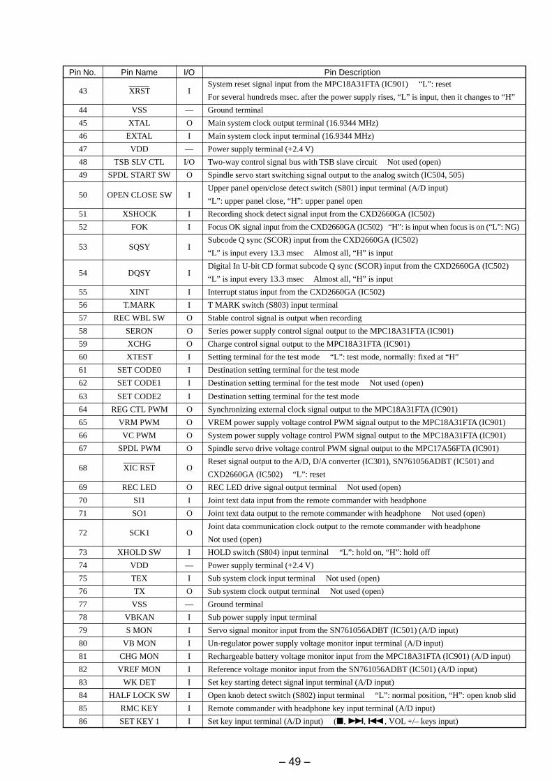
– 49 –
Pin No. Pin Name I/O Pin Description
43 XRST ISystem reset signal input from the MPC18A31FTA (IC901) “L”: reset
For several hundreds msec. after the power supply rises, “L” is input, then it changes to “H”
44 VSS — Ground terminal
45 XTAL O Main system clock output terminal (16.9344 MHz)
46 EXTAL I Main system clock input terminal (16.9344 MHz)
47 VDD — Power supply terminal (+2.4 V)
48 TSB SLV CTL I/O Two-way control signal bus with TSB slave circuit Not used (open)
49 SPDL START SW O Spindle servo start switching signal output to the analog switch (IC504, 505)
50 OPEN CLOSE SW IUpper panel open/close detect switch (S801) input terminal (A/D input)
“L”: upper panel close, “H”: upper panel open
51 XSHOCK I Recording shock detect signal input from the CXD2660GA (IC502)
52 FOK I Focus OK signal input from the CXD2660GA (IC502) “H”: is input when focus is on (“L”: NG)
53 SQSY ISubcode Q sync (SCOR) input from the CXD2660GA (IC502)
“L” is input every 13.3 msec Almost all, “H” is input
54 DQSY IDigital In U-bit CD format subcode Q sync (SCOR) input from the CXD2660GA (IC502)
“L” is input every 13.3 msec Almost all, “H” is input
55 XINT I Interrupt status input from the CXD2660GA (IC502)
56 T.MARK I T MARK switch (S803) input terminal
57 REC WBL SW O Stable control signal is output when recording
58 SERON O Series power supply control signal output to the MPC18A31FTA (IC901)
59 XCHG O Charge control signal output to the MPC18A31FTA (IC901)
60 XTEST I Setting terminal for the test mode “L”: test mode, normally: fixed at “H”
61 SET CODE0 I Destination setting terminal for the test mode
62 SET CODE1 I Destination setting terminal for the test mode Not used (open)
63 SET CODE2 I Destination setting terminal for the test mode
64 REG CTL PWM O Synchronizing external clock signal output to the MPC18A31FTA (IC901)
65 VRM PWM O VREM power supply voltage control PWM signal output to the MPC18A31FTA (IC901)
66 VC PWM O System power supply voltage control PWM signal output to the MPC18A31FTA (IC901)
67 SPDL PWM O Spindle servo drive voltage control PWM signal output to the MPC17A56FTA (IC901)
68 XIC RST OReset signal output to the A/D, D/A converter (IC301), SN761056ADBT (IC501) and
CXD2660GA (IC502) “L”: reset
69 REC LED O REC LED drive signal output terminal Not used (open)
70 SI1 I Joint text data input from the remote commander with headphone
71 SO1 O Joint text data output to the remote commander with headphone Not used (open)
72 SCK1 OJoint data communication clock output to the remote commander with headphone
Not used (open)
73 XHOLD SW I HOLD switch (S804) input terminal “L”: hold on, “H”: hold off
74 VDD — Power supply terminal (+2.4 V)
75 TEX I Sub system clock input terminal Not used (open)
76 TX O Sub system clock output terminal Not used (open)
77 VSS — Ground terminal
78 VBKAN I Sub power supply input terminal
79 S MON I Servo signal monitor input from the SN761056ADBT (IC501) (A/D input)
80 VB MON I Un-regulator power supply voltage monitor input terminal (A/D input)
81 CHG MON I Rechargeable battery voltage monitor input from the MPC18A31FTA (IC901) (A/D input)
82 VREF MON I Reference voltage monitor input from the SN761056ADBT (IC501) (A/D input)
83 WK DET I Set key starting detect signal input terminal (A/D input)
84 HALF LOCK SW I Open knob detect switch (S802) input terminal “L”: normal position, “H”: open knob slid
85 RMC KEY I Remote commander with headphone key input terminal (A/D input)
86 SET KEY 1 I Set key input terminal (A/D input) (x, >, ., VOL +/– keys input)
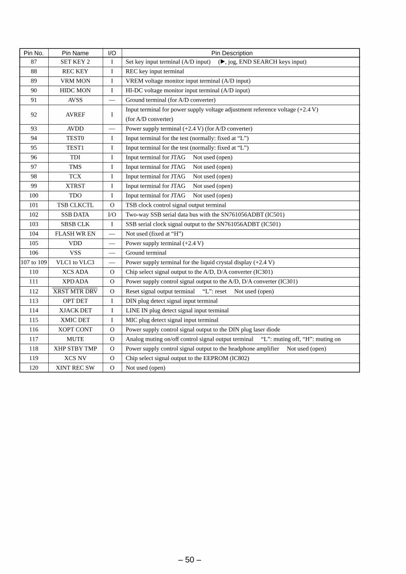
– 50 –
Pin No. Pin Name I/O Pin Description87 SET KEY 2 I Set key input terminal (A/D input) (B, jog, END SEARCH keys input)
88 REC KEY I REC key input terminal
89 VRM MON I VREM voltage monitor input terminal (A/D input)
90 HIDC MON I HI-DC voltage monitor input terminal (A/D input)
91 AVSS — Ground terminal (for A/D converter)
92 AVREF IInput terminal for power supply voltage adjustment reference voltage (+2.4 V)
(for A/D converter)
93 AVDD — Power supply terminal (+2.4 V) (for A/D converter)
94 TEST0 I Input terminal for the test (normally: fixed at “L”)
95 TEST1 I Input terminal for the test (normally: fixed at “L”)
96 TDI I Input terminal for JTAG Not used (open)
97 TMS I Input terminal for JTAG Not used (open)
98 TCX I Input terminal for JTAG Not used (open)
99 XTRST I Input terminal for JTAG Not used (open)
100 TDO I Input terminal for JTAG Not used (open)
101 TSB CLKCTL O TSB clock control signal output terminal
102 SSB DATA I/O Two-way SSB serial data bus with the SN761056ADBT (IC501)
103 SBSB CLK I SSB serial clock signal output to the SN761056ADBT (IC501)
104 FLASH WR EN — Not used (fixed at “H”)
105 VDD — Power supply terminal (+2.4 V)
106 VSS — Ground terminal
107 to 109 VLC1 to VLC3 — Power supply terminal for the liquid crystal display (+2.4 V)
110 XCS ADA O Chip select signal output to the A/D, D/A converter (IC301)
111 XPD ADA O Power supply control signal output to the A/D, D/A converter (IC301)
112 XRST MTR DRV O Reset signal output terminal “L”: reset Not used (open)
113 OPT DET I DIN plug detect signal input terminal
114 XJACK DET I LINE IN plug detect signal input terminal
115 XMIC DET I MIC plug detect signal input terminal
116 XOPT CONT O Power supply control signal output to the DIN plug laser diode
117 MUTE O Analog muting on/off control signal output terminal “L”: muting off, “H”: muting on
118 XHP STBY TMP O Power supply control signal output to the headphone amplifier Not used (open)
119 XCS NV O Chip select signal output to the EEPROM (IC802)
120 XINT REC SW O Not used (open)
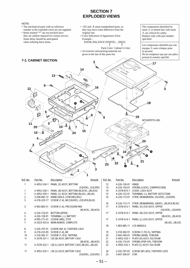
– 51 –
1
32
3
4
5
6
1125
10
10
10
129
13
14
16
7
2415
89
3 17
3
18
19MT-MZR70-165
20
212223 9
9
A
BA
BC
C
SECTION 7EXPLODED VIEWS
NOTE:• The mechanical parts with no reference
number in the exploded views are not supplied.• Items marked “*” are not stocked since
they are seldom required for routine service.Some delay should be anticipatedwhen ordering these items.
• -XX and -X mean standardized parts, sothey may have some difference from theoriginal one.
• Color Indication of Appearance PartsExample :
KNOB, BALANCE (WHITE) ... (RED)
Parts Color Cabinet’s Color• Accessories and packing materials are
given in the last of this parts list.
Ref. No. Part No. Description Remark
7-1. CABINET SECTION
Ref. No. Part No. Description Remark
1 X-4952-534-1 PANEL (S) ASSY, BOTTOM(SILVER)...(SILVER)
1 X-4952-538-1 PANEL (B) ASSY, BOTTOM (BLACK)...(BLACK)1 X-4952-539-1 PANEL (L) ASSY, BOTTOM (BLUE)...(BLUE)2 3-938-805-72 KNOB (HOLD, SYNCHRO REC)3 4-218-229-17 SCREW (1.4), MI (SILVER)...(SILVER,BLUE)
3 4-963-883-51 SCREW (1.4), PRECISION PAN (BLACK)...(BLACK)
4 4-226-124-01 BUTTON (OPEN)5 4-226-128-01 TERMINAL (–), BATTERY6 4-995-271-01 SCREW (MD), STEP7 A-3323-423-A MAIN BOARD, COMPLETE
8 3-335-797-91 SCREW (M1.4), TOOTHED LOCK9 4-218-233-05 SCREW (1.4), MI10 3-318-382-21 SCREW (1.7X3), TAPPING11 X-3378-331-1 LID (B) ASSY, BATTERY CASE
(BLACK)...(BLACK)11 X-3378-332-1 LID (L) ASSY, BATTERY CASE (BLUE)...(BLUE)
11 X-4952-535-1 LID (S) ASSY, BATTERY CASE (SILVER)...(SILVER)
12 4-226-126-01 HINGE13 4-226-120-01 SPRING (LOCK), COMPRESSION14 X-3378-815-1 LEVER, LOCK ASSY15 4-226-122-01 TERMINAL (+), BATTERY DETECTION16 4-226-113-01 STRIP, ORNAMENTAL (SILVER)...(SILVER)
16 4-226-113-11 STRIP, ORNAMENTAL (GRAY)...(BLACK,BLUE)17 X-3378-612-1 PANEL (S) (SV) ASSY, UPPER
(SILVER)...(SILVER)17 X-3378-613-1 PANEL (B) (SV) ASSY, UPPER
(BLACK)...(BLACK)17 X-3378-614-1 PANEL (L) (SV) ASSY, UPPER
(BLUE)...(BLUE)18 1-803-885-11 LCD MODULE
19 3-318-382-91 SCREW (1.7X2.5), TAPPING20 3-043-549-01 SPRING (ARM), TENSION21 X-4952-533-1 PLATE (R) ASSY, FULCRUM22 4-226-116-01 SPRING (POP-UP), TORSION23 X-4952-532-1 PLATE (L) ASSY, FULCRUM
24 3-335-797-81 SCREW (M1.4X5), TOOTHED LOCK25 3-047-350-01 STAY
R R
The components identified bymark 0 or dotted line with mark0 are critical for safety.Replace only with part numberspecified.
Les composants identifiés par unemarque 0 sont critiques pourla sécurité.Ne les remplacer que par une piéceportant le numéro spécifié.
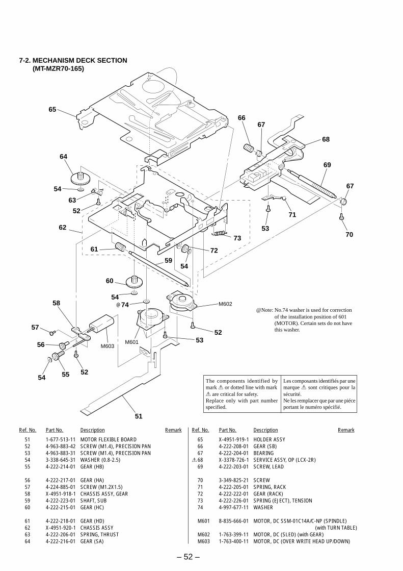
– 52 –
6566
67
68
69
67
7053
71
72
73
5459
M602
5253M601
51
M603
525554
56
57
58
62
52
63
54
64
5474
60
61
7-2. MECHANISM DECK SECTION(MT-MZR70-165)
Ref. No. Part No. Description Remark Ref. No. Part No. Description Remark
51 1-677-513-11 MOTOR FLEXIBLE BOARD52 4-963-883-42 SCREW (M1.4), PRECISION PAN53 4-963-883-31 SCREW (M1.4), PRECISION PAN54 3-338-645-31 WASHER (0.8-2.5)55 4-222-214-01 GEAR (HB)
56 4-222-217-01 GEAR (HA)57 4-224-885-01 SCREW (M1.2X1.5)58 X-4951-918-1 CHASSIS ASSY, GEAR59 4-222-223-01 SHAFT, SUB60 4-222-215-01 GEAR (HC)
61 4-222-218-01 GEAR (HD)62 X-4951-920-1 CHASSIS ASSY63 4-222-206-01 SPRING, THRUST64 4-222-216-01 GEAR (SA)
65 X-4951-919-1 HOLDER ASSY66 4-222-208-01 GEAR (SB)67 4-222-204-01 BEARING
068 X-3378-726-1 SERVICE ASSY, OP (LCX-2R)69 4-222-203-01 SCREW, LEAD
70 3-349-825-21 SCREW71 4-222-205-01 SPRING, RACK72 4-222-222-01 GEAR (RACK)73 4-222-226-01 SPRING (EJECT), TENSION74 4-997-677-11 WASHER
M601 8-835-666-01 MOTOR, DC SSM-01C14A/C-NP (SPINDLE)(with TURN TABLE)
M602 1-763-399-11 MOTOR, DC (SLED) (with GEAR)M603 1-763-400-11 MOTOR, DC (OVER WRITE HEAD UP/DOWN)
The components identified bymark 0 or dotted line with mark0 are critical for safety.Replace only with part numberspecified.
Les composants identifiés par unemarque 0 sont critiques pour lasécurité.Ne les remplacer que par une piéceportant le numéro spécifié.
@Note: No.74 washer is used for correctionof the installation position of 601(MOTOR). Certain sets do not havethis washer.
@
– 53 –
SECTION 8ELECTRICAL PARTS LIST
NOTE:• Due to standardization, replacements in
the parts list may be different from theparts specified in the diagrams or thecomponents used on the set.
• -XX and -X mean standardized parts, sothey may have some difference from theoriginal one.
• RESISTORSAll resistors are in ohms.METAL:Metal-film resistor.METAL OXIDE: Metal oxide-film resistor.F:nonflammable
• CAPACITORSuF : µF
• COILSuH : µH
• Items marked “*” are not stocked sincethey are seldom required for routine service.Some delay should be anticipatedwhen ordering these items.
• SEMICONDUCTORSIn each case, u : µ, for example:uA.. : µA.. uPA.. : µPA..uPB.. : µPB.. uPC.. : µPC.. uPD.. : µPD..
• AbbreviationAR : Argentine modelAUS : Australian modelCH : Chinese modelCND : Canadian modelEE : East European modelFR : French modelHK : Hong Kong modelJE : Tourist modelKR : Korea model
Ref. No. Part No. Description Remark Ref. No. Part No. Description Remark
A-3323-423-A MAIN BOARD, COMPLETE*********************
< CAPACITOR >
C101 1-115-467-11 CERAMIC CHIP 0.22uF 10% 10VC102 1-107-820-11 CERAMIC CHIP 0.1uF 16VC103 1-135-210-11 TANTALUM CHIP 4.7uF 20% 10VC106 1-125-899-11 TANTAL. CHIP 220uF 20% 4VC108 1-125-837-11 CERAMIC CHIP 1uF 10% 6.3V
C110 1-125-837-11 CERAMIC CHIP 1uF 10% 6.3VC111 1-164-874-11 CERAMIC CHIP 100PF 5% 16VC112 1-135-259-11 TANTAL. CHIP 10uF 20% 6.3VC113 1-110-569-11 TANTAL. CHIP 47uF 20% 4VC116 1-164-937-11 CERAMIC CHIP 0.001uF 10% 16V
C117 1-125-985-11 CERAMIC CHIP 0.47uF 10% 25VC118 1-164-939-11 CERAMIC CHIP 0.0022uF 10% 16VC120 1-164-942-11 CERAMIC CHIP 0.0068uF 10% 16VC122 1-125-838-11 CERAMIC CHIP 2.2uF 10% 6.3VC123 1-164-937-11 CERAMIC CHIP 0.001uF 10% 16V
C124 1-164-937-11 CERAMIC CHIP 0.001uF 10% 16VC201 1-115-467-11 CERAMIC CHIP 0.22uF 10% 10VC202 1-107-820-11 CERAMIC CHIP 0.1uF 16VC203 1-135-210-11 TANTALUM CHIP 4.7uF 20% 10VC206 1-125-899-11 TANTAL. CHIP 220uF 20% 4V
C208 1-125-837-11 CERAMIC CHIP 1uF 10% 6.3VC210 1-125-837-11 CERAMIC CHIP 1uF 10% 6.3VC211 1-164-874-11 CERAMIC CHIP 100PF 5% 16VC212 1-135-259-11 TANTAL. CHIP 10uF 20% 6.3VC213 1-110-569-11 TANTAL. CHIP 47uF 20% 4V
C216 1-164-937-11 CERAMIC CHIP 0.001uF 10% 16VC217 1-125-985-11 CERAMIC CHIP 0.47uF 10% 25VC218 1-164-939-11 CERAMIC CHIP 0.0022uF 10% 16VC220 1-164-942-11 CERAMIC CHIP 0.0068uF 10% 16VC222 1-125-838-11 CERAMIC CHIP 2.2uF 10% 6.3V
C223 1-164-937-11 CERAMIC CHIP 0.001uF 10% 16VC224 1-164-937-11 CERAMIC CHIP 0.001uF 10% 16VC301 1-107-820-11 CERAMIC CHIP 0.1uF 16VC303 1-107-820-11 CERAMIC CHIP 0.1uF 16VC304 1-135-259-11 TANTAL. CHIP 10uF 20% 6.3V
C306 1-135-259-11 TANTAL. CHIP 10uF 20% 6.3VC307 1-110-569-11 TANTAL. CHIP 47uF 20% 4VC308 1-107-820-11 CERAMIC CHIP 0.1uF 16VC310 1-164-943-11 CERAMIC CHIP 0.01uF 10% 16VC311 1-125-777-11 CERAMIC CHIP 0.1uF 10% 10V
C312 1-164-949-11 CERAMIC CHIP 0.047uF 16VC315 1-110-569-11 TANTAL. CHIP 47uF 20% 4VC316 1-125-777-11 CERAMIC CHIP 0.1uF 10% 10VC317 1-125-777-11 CERAMIC CHIP 0.1uF 10% 10VC318 1-125-777-11 CERAMIC CHIP 0.1uF 10% 10V
C319 1-164-943-11 CERAMIC CHIP 0.01uF 10% 16VC320 1-135-259-11 TANTAL. CHIP 10uF 20% 6.3VC321 1-125-777-11 CERAMIC CHIP 0.1uF 10% 10VC322 1-110-569-11 TANTAL. CHIP 47uF 20% 4VC323 1-135-259-11 TANTAL. CHIP 10uF 20% 6.3V
C324 1-104-847-11 TANTAL. CHIP 22uF 20% 4VC330 1-107-820-11 CERAMIC CHIP 0.1uF 16VC331 1-125-777-11 CERAMIC CHIP 0.1uF 10% 10VC332 1-135-259-11 TANTAL. CHIP 10uF 20% 6.3VC333 1-135-259-11 TANTAL. CHIP 10uF 20% 6.3V
C334 1-125-777-11 CERAMIC CHIP 0.1uF 10% 10VC335 1-125-837-11 CERAMIC CHIP 1uF 10% 6.3VC336 1-135-181-21 TANTALUM CHIP 4.7uF 20% 6.3VC337 1-110-501-11 CERAMIC CHIP 0.33uF 10% 16VC338 1-135-259-11 TANTAL. CHIP 10uF 20% 6.3V
C339 1-110-501-11 CERAMIC CHIP 0.33uF 10% 16VC340 1-125-777-11 CERAMIC CHIP 0.1uF 10% 10VC501 1-125-777-11 CERAMIC CHIP 0.1uF 10% 10VC502 1-127-772-81 CERAMIC CHIP 0.033uF 10% 10VC503 1-164-940-11 CERAMIC CHIP 0.0033uF 10% 16V
C504 1-164-940-11 CERAMIC CHIP 0.0033uF 10% 16VC505 1-164-943-11 CERAMIC CHIP 0.01uF 10% 16VC506 1-127-772-81 CERAMIC CHIP 0.033uF 10% 10VC507 1-125-777-11 CERAMIC CHIP 0.1uF 10% 10VC508 1-164-858-11 CERAMIC CHIP 22PF 5% 16V
C509 1-164-940-11 CERAMIC CHIP 0.0033uF 10% 16VC510 1-125-777-11 CERAMIC CHIP 0.1uF 10% 10VC511 1-164-845-11 CERAMIC CHIP 5PF 0.25PF 16VC512 1-164-938-11 CERAMIC CHIP 0.0015uF 10% 16VC513 1-127-772-81 CERAMIC CHIP 0.033uF 10% 10V
C514 1-125-777-11 CERAMIC CHIP 0.1uF 10% 10VC515 1-125-777-11 CERAMIC CHIP 0.1uF 10% 10VC516 1-164-845-11 CERAMIC CHIP 5PF 0.25PF 16VC517 1-164-940-11 CERAMIC CHIP 0.0033uF 10% 16VC519 1-125-777-11 CERAMIC CHIP 0.1uF 10% 10V
C520 1-107-819-11 CERAMIC CHIP 0.022uF 10% 16VC521 1-119-923-81 CERAMIC CHIP 0.047uF 10% 10VC522 1-164-943-11 CERAMIC CHIP 0.01uF 10% 16VC524 1-110-569-11 TANTAL. CHIP 47uF 20% 4VC525 1-164-943-11 CERAMIC CHIP 0.01uF 10% 16V
MAIN
The components identified bymark 0 or dotted line with mark0 are critical for safety.Replace only with part numberspecified.
Les composants identifiés par unemarque 0 sont critiques pourla sécurité.Ne les remplacer que par une piéceportant le numéro spécifié.
When indicating parts by referencenumber, please include the board.
– 54 –
C526 1-164-943-11 CERAMIC CHIP 0.01uF 10% 16VC527 1-164-854-11 CERAMIC CHIP 15PF 5% 16VC528 1-164-854-11 CERAMIC CHIP 15PF 5% 16VC529 1-104-847-11 TANTAL. CHIP 22uF 20% 4VC530 1-110-569-11 TANTAL. CHIP 47uF 20% 4V
C531 1-164-943-11 CERAMIC CHIP 0.01uF 10% 16VC532 1-164-943-11 CERAMIC CHIP 0.01uF 10% 16VC533 1-164-245-11 CERAMIC CHIP 0.015uF 10% 25VC534 1-117-863-11 CERAMIC CHIP 0.47uF 10% 6.3VC535 1-164-935-11 CERAMIC CHIP 470PF 10% 16V
C536 1-117-863-11 CERAMIC CHIP 0.47uF 10% 6.3VC537 1-164-943-11 CERAMIC CHIP 0.01uF 10% 16VC600 1-125-777-11 CERAMIC CHIP 0.1uF 10% 10VC601 1-131-862-91 TANTAL. CHIP 47uF 20% 4VC602 1-109-813-11 CAP-CHIP 100PF 5% 100V
C605 1-131-862-91 TANTAL. CHIP 47uF 20% 4VC609 1-125-777-11 CERAMIC CHIP 0.1uF 10% 10VC610 1-125-777-11 CERAMIC CHIP 0.1uF 10% 10VC611 1-125-777-11 CERAMIC CHIP 0.1uF 10% 10VC612 1-107-819-11 CERAMIC CHIP 0.022uF 10% 16V
C613 1-104-851-11 TANTAL. CHIP 10uF 20% 10VC614 1-131-862-91 TANTAL. CHIP 47uF 20% 4VC615 1-135-210-11 TANTAL. CHIP 4.7uF 20% 10VC616 1-125-777-11 CERAMIC CHIP 0.1uF 10% 10VC617 1-127-772-81 CERAMIC CHIP 0.033uF 10% 10V
C618 1-127-772-81 CERAMIC CHIP 0.033uF 10% 10VC619 1-127-772-81 CERAMIC CHIP 0.033uF 10% 10VC620 1-135-211-11 TANTAL. CHIP 6.8uF 20% 6.3VC621 1-104-912-11 TANTAL. CHIP 3.3uF 20% 6.3VC622 1-135-211-11 TANTAL. CHIP 6.8uF 20% 6.3V
C623 1-104-912-11 TANTAL. CHIP 3.3uF 20% 6.3VC624 1-125-777-11 CERAMIC CHIP 0.1uF 10% 10VC625 1-125-777-11 CERAMIC CHIP 0.1uF 10% 10VC629 1-125-777-11 CERAMIC CHIP 0.1uF 10% 10VC630 1-125-777-11 CERAMIC CHIP 0.1uF 10% 10V
C631 1-125-777-11 CERAMIC CHIP 0.1uF 10% 10VC632 1-125-777-11 CERAMIC CHIP 0.1uF 10% 10VC633 1-128-964-11 TANTAL. CHIP 100uF 20% 6.3VC638 1-125-837-11 CERAMIC CHIP 1uF 10% 6.3VC640 1-131-726-11 TANTAL. CHIP 33uF 20% 6.3V
C801 1-164-943-11 CERAMIC CHIP 0.01uF 10% 16VC806 1-104-847-11 TANTAL. CHIP 22uF 20% 4VC807 1-164-943-11 CERAMIC CHIP 0.01uF 10% 16VC810 1-164-937-11 CERAMIC CHIP 0.001uF 10% 16VC901 1-164-941-11 CERAMIC CHIP 0.0047uF 10% 16V
C902 1-164-943-11 CERAMIC CHIP 0.01uF 10% 16VC903 1-128-964-11 TANTAL. CHIP 100uF 20% 6.3VC904 1-164-943-11 CERAMIC CHIP 0.01uF 10% 16VC905 1-164-937-11 CERAMIC CHIP 0.001uF 10% 16VC906 1-135-259-11 TANTAL. CHIP 10uF 20% 6.3V
C910 1-107-819-11 CERAMIC CHIP 0.022uF 10% 16VC911 1-135-259-11 TANTAL. CHIP 10uF 20% 6.3VC913 1-135-259-11 TANTAL. CHIP 10uF 20% 6.3V
Ref. No. Part No. Description Remark Ref. No. Part No. Description Remark
MAIN
C915 1-115-169-11 TANTALUM 10uF 20% 6.3VC916 1-110-569-11 TANTAL. CHIP 47uF 20% 4VC917 1-128-964-11 TANTAL. CHIP 100uF 20% 6.3VC918 1-107-819-11 CERAMIC CHIP 0.022uF 10% 16VC919 1-109-982-11 CERAMIC CHIP 1uF 10% 10V
C920 1-125-837-11 CERAMIC CHIP 1uF 10% 6.3VC921 1-164-943-11 CERAMIC CHIP 0.01uF 10% 16VC922 1-125-777-11 CERAMIC CHIP 0.1uF 10% 10VC923 1-164-933-11 CERAMIC CHIP 220PF 10% 16VC925 1-164-943-11 CERAMIC CHIP 0.01uF 10% 16V
C926 1-119-923-81 CERAMIC CHIP 0.047uF 10% 10VC929 1-119-923-81 CERAMIC CHIP 0.047uF 10% 10VC930 1-125-777-11 CERAMIC CHIP 0.1uF 10% 10VC932 1-164-937-11 CERAMIC CHIP 0.001uF 10% 16VC933 1-164-937-11 CERAMIC CHIP 0.001uF 10% 16V
C934 1-164-937-11 CERAMIC CHIP 0.001uF 10% 16VC935 1-164-937-11 CERAMIC CHIP 0.001uF 10% 16VC936 1-109-982-11 CERAMIC CHIP 1uF 10% 10VC937 1-126-246-11 ELECT CHIP 220uF 20% 4VC938 1-126-246-11 ELECT CHIP 220uF 20% 4V
C939 1-107-826-11 CERAMIC CHIP 0.1uF 10% 16VC1001 1-115-169-11 TANTALUM 10uF 20% 6.3VC1002 1-127-772-81 CERAMIC CHIP 0.033uF 10% 10VC1003 1-127-772-81 CERAMIC CHIP 0.033uF 10% 10VC1004 1-164-939-11 CERAMIC CHIP 0.0022uF 10% 16V
< CONNECTOR >
CN501 1-573-360-21 CONNECTOR, FFC/FPC 20PCN601 1-785-355-21 CONNECTOR, FFC/FPC (ZIF) 5PCN602 1-573-355-11 CONNECTOR, FFC/FPC 15PCN801 1-573-354-11 CONNECTOR, FFC/FPC 14P
< DIODE >
D101 8-719-056-72 DIODE UDZ-TE-17-2.4BD201 8-719-056-72 DIODE UDZ-TE-17-2.4BD301 8-719-066-17 DIODE FTZ6.8E-T148D302 8-719-066-17 DIODE FTZ6.8E-T148D501 8-719-421-27 DIODE MA728
D600 8-719-072-10 DIODE FS05J10-TPD601 8-719-072-10 DIODE FS05J10-TPD602 8-719-066-34 DIODE RB461F-T106D901 8-719-420-51 DIODE MA729D902 8-719-072-26 DIODE FS1J3-TP
D903 8-719-072-26 DIODE FS1J3-TPD905 8-719-074-74 DIODE MA3XD15001S0D906 8-719-074-74 DIODE MA3XD15001S0D907 8-719-072-26 DIODE FS1J3-TP
< FERRITE BEAD >
FB301 1-414-228-11 FERRITE BEAD INDUCTORFB302 1-414-228-11 FERRITE BEAD INDUCTORFB303 1-414-228-11 FERRITE BEAD INDUCTORFB304 1-414-228-11 FERRITE BEAD INDUCTORFB501 1-414-228-11 FERRITE BEAD INDUCTOR
– 55 –
Ref. No. Part No. Description Remark Ref. No. Part No. Description Remark
FB502 1-414-228-11 FERRITE BEAD INDUCTORFB503 1-414-228-11 FERRITE BEAD INDUCTORFB504 1-414-228-11 FERRITE BEAD INDUCTORFB505 1-414-228-11 FERRITE BEAD INDUCTORFB601 1-500-329-21 FERRITE BEAD INDUCTOR
< IC >
IC301 8-759-584-59 IC AK4517A-VQ-LIC302 8-759-656-15 IC NJM2173IC303 8-759-598-15 IC TA2131FL-ELIC501 8-759-661-14 IC SN761056ADBT
@ IC502 8-752-397-66 IC CXD2660GA
IC504 8-759-647-75 IC TC7W66FK(TE85R)IC505 8-759-647-75 IC TC7W66FK(TE85R)IC601 8-759-642-14 IC MPC17A56FTAIC603 8-759-656-16 IC MPC18A21MTBIC604 8-759-358-40 IC TLC372CPW-E20
@ IC801 8-752-914-08 IC CXR701080-010GAIC802 8-759-445-94 IC AK6480AM-E2IC901 8-759-642-13 IC MPC18A31FTAIC902 8-759-652-23 IC RN5RG25AA-TRJ301 8-749-015-24 IC JFJ7001 (LINE IN (OPTICAL))
< JACK >
J302 1-779-881-11 JACK (i2)J303 1-779-881-21 JACK (MIC (PLUG IN POWER))J304 1-793-288-41 JACK (i1)J901 1-785-383-11 JACK, DC (POLARITY UNIFIED TYPE)
(DC IN 3V)
< COIL >
L301 1-469-535-21 INDUCTOR 10uHL302 1-469-535-21 INDUCTOR 10uHL501 1-469-535-21 INDUCTOR 10uHL502 1-469-535-21 INDUCTOR 10uHL601 1-410-389-31 INDUCTOR CHIP 47uH
L602 1-414-400-41 INDUCTOR 22uHL603 1-419-441-21 INDUCTOR 4.7uHL604 1-410-389-31 INDUCTOR CHIP 47uHL605 1-414-400-41 INDUCTOR 22uHL606 1-469-535-21 INDUCTOR 10uH
L801 1-469-535-21 INDUCTOR 10uHL901 1-414-398-11 INDUCTOR 10uHL902 1-469-426-21 INDUCTOR 100uHL903 1-469-367-21 INDUCTOR 10uHL904 1-419-257-21 INDUCTOR 22uH
L905 1-419-407-21 INDUCTOR 33uH
< FILTER >
LF901 1-416-405-21 FILTER, CHIP EMI (COMMON MODE)
< TRANSISTOR >
Q301 8-729-037-52 TRANSISTOR 2SD2216J-QR(TX).SO
Q302 8-729-046-49 FET FDV304PQ501 8-729-928-81 TRANSISTOR DTC144EEQ601 8-729-046-43 FET HAT2051T-ELQ602 8-729-046-42 FET HAT2050T-ELQ603 8-729-051-73 FET RDS035L03
Q901 8-729-046-44 FET ZDT6718TAQ902 8-729-046-45 FET SI2302DS-T1Q905 8-729-928-27 TRANSISTOR DTA144EEQ906 8-729-928-81 TRANSISTOR DTC144EEQ1001 8-729-922-10 TRANSISTOR 2SA1577-QR
< RESISTOR >
R101 1-216-835-11 METAL CHIP 15K 5% 1/16WR102 1-216-829-11 METAL CHIP 4.7K 5% 1/16WR103 1-216-797-11 METAL CHIP 10 5% 1/16WR104 1-216-819-11 METAL CHIP 680 5% 1/16WR108 1-216-829-11 METAL CHIP 4.7K 5% 1/16W
R109 1-216-864-11 METAL CHIP 0 5% 1/16WR111 1-218-891-11 METAL CHIP 68K 0.5% 1/16WR112 1-218-887-11 METAL CHIP 47K 0.5% 1/16WR118 1-218-867-11 METAL CHIP 6.8K 0.5% 1/16WR122 1-216-864-11 METAL CHIP 0 5% 1/16W
R123 1-216-864-11 METAL CHIP 0 5% 1/16WR201 1-216-835-11 METAL CHIP 15K 5% 1/16WR202 1-216-829-11 METAL CHIP 4.7K 5% 1/16WR203 1-216-797-11 METAL CHIP 10 5% 1/16WR204 1-216-819-11 METAL CHIP 680 5% 1/16W
R208 1-216-829-11 METAL CHIP 4.7K 5% 1/16WR209 1-216-864-11 METAL CHIP 0 5% 1/16WR211 1-218-891-11 METAL CHIP 68K 0.5% 1/16WR212 1-218-887-11 METAL CHIP 47K 0.5% 1/16WR218 1-218-867-11 METAL CHIP 6.8K 0.5% 1/16W
R222 1-216-864-11 METAL CHIP 0 5% 1/16WR223 1-216-864-11 METAL CHIP 0 5% 1/16WR301 1-216-803-11 METAL CHIP 33 5% 1/16WR302 1-216-821-11 METAL CHIP 1K 5% 1/16WR305 1-216-831-11 METAL CHIP 6.8K 5% 1/16W
R306 1-216-849-11 METAL CHIP 220K 5% 1/16WR307 1-216-809-11 METAL CHIP 100 5% 1/16WR317 1-216-809-11 METAL CHIP 100 5% 1/16WR318 1-216-809-11 METAL CHIP 100 5% 1/16WR319 1-216-809-11 METAL CHIP 100 5% 1/16W
R321 1-216-864-11 METAL CHIP 0 5% 1/16WR322 1-216-864-11 METAL CHIP 0 5% 1/16WR325 1-216-797-11 METAL CHIP 10 5% 1/16WR502 1-216-833-11 RES-CHIP 10K 5% 1/16WR503 1-216-864-11 METAL CHIP 0 5% 1/16W
R505 1-216-864-11 METAL CHIP 0 5% 1/16WR506 1-216-864-11 METAL CHIP 0 5% 1/16WR507 1-216-839-11 METAL CHIP 33K 5% 1/16WR508 1-216-809-11 METAL CHIP 100 5% 1/16WR509 1-216-817-11 METAL CHIP 470 5% 1/16W
R510 1-216-813-11 METAL CHIP 220 5% 1/16W
MAIN
@ Replacement of CXD2660GA (IC502), CXR701080(IC801) used in this set requires a special tool.Therfore, it cannot be replaced.
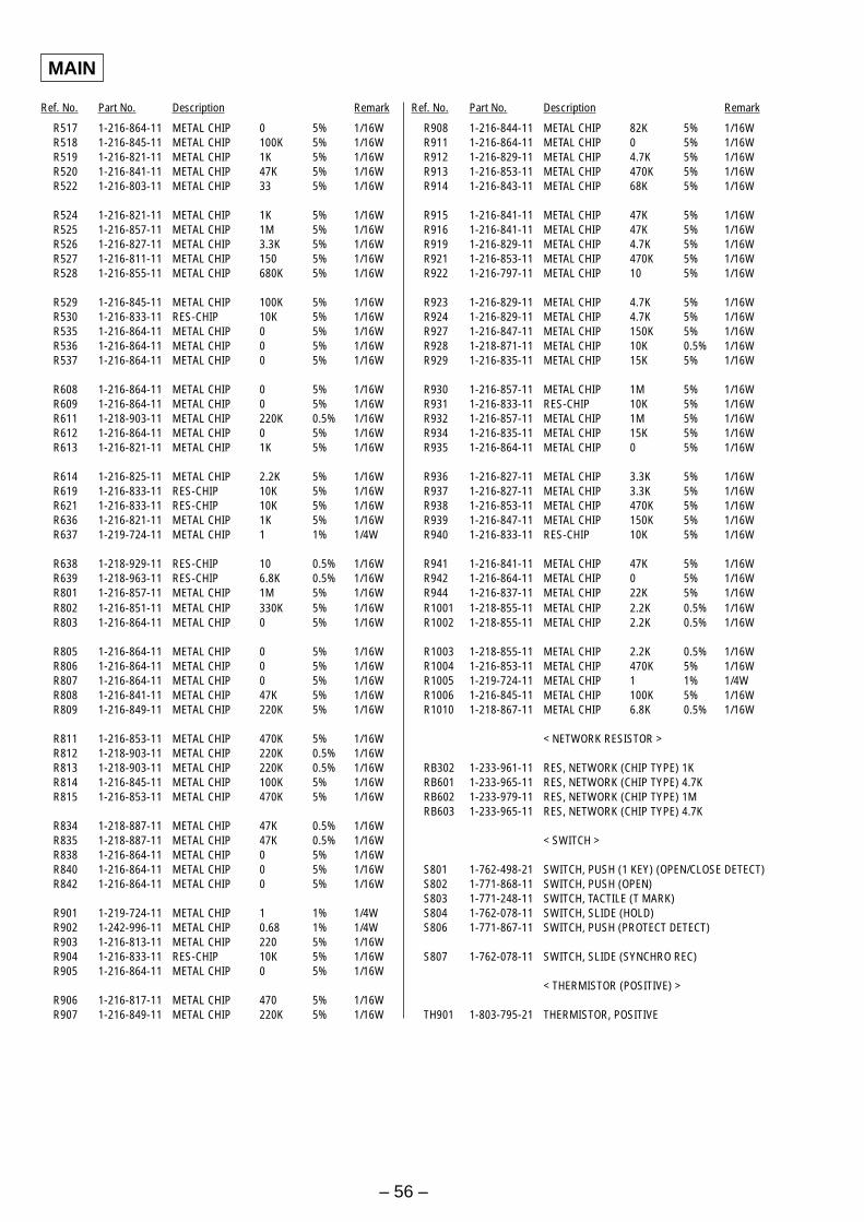
– 56 –
Ref. No. Part No. Description Remark
R517 1-216-864-11 METAL CHIP 0 5% 1/16WR518 1-216-845-11 METAL CHIP 100K 5% 1/16WR519 1-216-821-11 METAL CHIP 1K 5% 1/16WR520 1-216-841-11 METAL CHIP 47K 5% 1/16WR522 1-216-803-11 METAL CHIP 33 5% 1/16W
R524 1-216-821-11 METAL CHIP 1K 5% 1/16WR525 1-216-857-11 METAL CHIP 1M 5% 1/16WR526 1-216-827-11 METAL CHIP 3.3K 5% 1/16WR527 1-216-811-11 METAL CHIP 150 5% 1/16WR528 1-216-855-11 METAL CHIP 680K 5% 1/16W
R529 1-216-845-11 METAL CHIP 100K 5% 1/16WR530 1-216-833-11 RES-CHIP 10K 5% 1/16WR535 1-216-864-11 METAL CHIP 0 5% 1/16WR536 1-216-864-11 METAL CHIP 0 5% 1/16WR537 1-216-864-11 METAL CHIP 0 5% 1/16W
R608 1-216-864-11 METAL CHIP 0 5% 1/16WR609 1-216-864-11 METAL CHIP 0 5% 1/16WR611 1-218-903-11 METAL CHIP 220K 0.5% 1/16WR612 1-216-864-11 METAL CHIP 0 5% 1/16WR613 1-216-821-11 METAL CHIP 1K 5% 1/16W
R614 1-216-825-11 METAL CHIP 2.2K 5% 1/16WR619 1-216-833-11 RES-CHIP 10K 5% 1/16WR621 1-216-833-11 RES-CHIP 10K 5% 1/16WR636 1-216-821-11 METAL CHIP 1K 5% 1/16WR637 1-219-724-11 METAL CHIP 1 1% 1/4W
R638 1-218-929-11 RES-CHIP 10 0.5% 1/16WR639 1-218-963-11 RES-CHIP 6.8K 0.5% 1/16WR801 1-216-857-11 METAL CHIP 1M 5% 1/16WR802 1-216-851-11 METAL CHIP 330K 5% 1/16WR803 1-216-864-11 METAL CHIP 0 5% 1/16W
R805 1-216-864-11 METAL CHIP 0 5% 1/16WR806 1-216-864-11 METAL CHIP 0 5% 1/16WR807 1-216-864-11 METAL CHIP 0 5% 1/16WR808 1-216-841-11 METAL CHIP 47K 5% 1/16WR809 1-216-849-11 METAL CHIP 220K 5% 1/16W
R811 1-216-853-11 METAL CHIP 470K 5% 1/16WR812 1-218-903-11 METAL CHIP 220K 0.5% 1/16WR813 1-218-903-11 METAL CHIP 220K 0.5% 1/16WR814 1-216-845-11 METAL CHIP 100K 5% 1/16WR815 1-216-853-11 METAL CHIP 470K 5% 1/16W
R834 1-218-887-11 METAL CHIP 47K 0.5% 1/16WR835 1-218-887-11 METAL CHIP 47K 0.5% 1/16WR838 1-216-864-11 METAL CHIP 0 5% 1/16WR840 1-216-864-11 METAL CHIP 0 5% 1/16WR842 1-216-864-11 METAL CHIP 0 5% 1/16W
R901 1-219-724-11 METAL CHIP 1 1% 1/4WR902 1-242-996-11 METAL CHIP 0.68 1% 1/4WR903 1-216-813-11 METAL CHIP 220 5% 1/16WR904 1-216-833-11 RES-CHIP 10K 5% 1/16WR905 1-216-864-11 METAL CHIP 0 5% 1/16W
R906 1-216-817-11 METAL CHIP 470 5% 1/16WR907 1-216-849-11 METAL CHIP 220K 5% 1/16W
R908 1-216-844-11 METAL CHIP 82K 5% 1/16WR911 1-216-864-11 METAL CHIP 0 5% 1/16WR912 1-216-829-11 METAL CHIP 4.7K 5% 1/16WR913 1-216-853-11 METAL CHIP 470K 5% 1/16WR914 1-216-843-11 METAL CHIP 68K 5% 1/16W
R915 1-216-841-11 METAL CHIP 47K 5% 1/16WR916 1-216-841-11 METAL CHIP 47K 5% 1/16WR919 1-216-829-11 METAL CHIP 4.7K 5% 1/16WR921 1-216-853-11 METAL CHIP 470K 5% 1/16WR922 1-216-797-11 METAL CHIP 10 5% 1/16W
R923 1-216-829-11 METAL CHIP 4.7K 5% 1/16WR924 1-216-829-11 METAL CHIP 4.7K 5% 1/16WR927 1-216-847-11 METAL CHIP 150K 5% 1/16WR928 1-218-871-11 METAL CHIP 10K 0.5% 1/16WR929 1-216-835-11 METAL CHIP 15K 5% 1/16W
R930 1-216-857-11 METAL CHIP 1M 5% 1/16WR931 1-216-833-11 RES-CHIP 10K 5% 1/16WR932 1-216-857-11 METAL CHIP 1M 5% 1/16WR934 1-216-835-11 METAL CHIP 15K 5% 1/16WR935 1-216-864-11 METAL CHIP 0 5% 1/16W
R936 1-216-827-11 METAL CHIP 3.3K 5% 1/16WR937 1-216-827-11 METAL CHIP 3.3K 5% 1/16WR938 1-216-853-11 METAL CHIP 470K 5% 1/16WR939 1-216-847-11 METAL CHIP 150K 5% 1/16WR940 1-216-833-11 RES-CHIP 10K 5% 1/16W
R941 1-216-841-11 METAL CHIP 47K 5% 1/16WR942 1-216-864-11 METAL CHIP 0 5% 1/16WR944 1-216-837-11 METAL CHIP 22K 5% 1/16WR1001 1-218-855-11 METAL CHIP 2.2K 0.5% 1/16WR1002 1-218-855-11 METAL CHIP 2.2K 0.5% 1/16W
R1003 1-218-855-11 METAL CHIP 2.2K 0.5% 1/16WR1004 1-216-853-11 METAL CHIP 470K 5% 1/16WR1005 1-219-724-11 METAL CHIP 1 1% 1/4WR1006 1-216-845-11 METAL CHIP 100K 5% 1/16WR1010 1-218-867-11 METAL CHIP 6.8K 0.5% 1/16W
< NETWORK RESISTOR >
RB302 1-233-961-11 RES, NETWORK (CHIP TYPE) 1KRB601 1-233-965-11 RES, NETWORK (CHIP TYPE) 4.7KRB602 1-233-979-11 RES, NETWORK (CHIP TYPE) 1MRB603 1-233-965-11 RES, NETWORK (CHIP TYPE) 4.7K
< SWITCH >
S801 1-762-498-21 SWITCH, PUSH (1 KEY) (OPEN/CLOSE DETECT)S802 1-771-868-11 SWITCH, PUSH (OPEN)S803 1-771-248-11 SWITCH, TACTILE (T MARK)S804 1-762-078-11 SWITCH, SLIDE (HOLD)S806 1-771-867-11 SWITCH, PUSH (PROTECT DETECT)
S807 1-762-078-11 SWITCH, SLIDE (SYNCHRO REC)
< THERMISTOR (POSITIVE) >
TH901 1-803-795-21 THERMISTOR, POSITIVE
Ref. No. Part No. Description Remark
MAIN
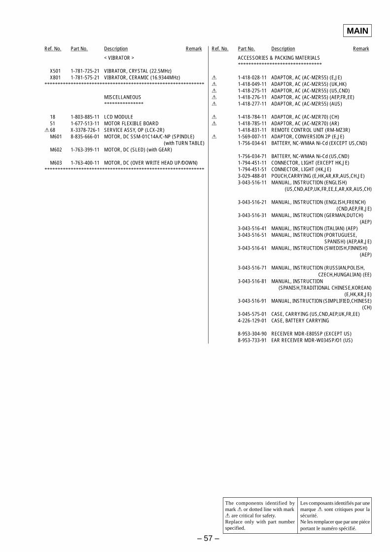
– 57 –
Ref. No. Part No. Description Remark
< VIBRATOR >
X501 1-781-725-21 VIBRATOR, CRYSTAL (22.5MHz)X801 1-781-575-21 VIBRATOR, CERAMIC (16.9344MHz)
*************************************************************
MISCELLANEOUS***************
18 1-803-885-11 LCD MODULE51 1-677-513-11 MOTOR FLEXIBLE BOARD
068 X-3378-726-1 SERVICE ASSY, OP (LCX-2R)M601 8-835-666-01 MOTOR, DC SSM-01C14A/C-NP (SPINDLE)
(with TURN TABLE)M602 1-763-399-11 MOTOR, DC (SLED) (with GEAR)
M603 1-763-400-11 MOTOR, DC (OVER WRITE HEAD UP/DOWN)*************************************************************
MAIN
The components identified bymark 0 or dotted line with mark0 are critical for safety.Replace only with part numberspecified.
Les composants identifiés par unemarque 0 sont critiques pour lasécurité.Ne les remplacer que par une piéceportant le numéro spécifié.
Ref. No. Part No. Description Remark
ACCESSORIES & PACKING MATERIALS********************************
0 1-418-028-11 ADAPTOR, AC (AC-MZR55) (E,JE)0 1-418-049-11 ADAPTOR, AC (AC-MZR55) (UK,HK)0 1-418-275-11 ADAPTOR, AC (AC-MZR55) (US,CND)0 1-418-276-11 ADAPTOR, AC (AC-MZR55) (AEP,FR,EE)0 1-418-277-11 ADAPTOR, AC (AC-MZR55) (AUS)
0 1-418-784-11 ADAPTOR, AC (AC-MZR70) (CH)0 1-418-785-11 ADAPTOR, AC (AC-MZR70) (AR)
1-418-831-11 REMOTE CONTROL UNIT (RM-MZ3R)0 1-569-007-11 ADAPTOR, CONVERSION 2P (E,JE)
1-756-034-61 BATTERY, NC-WMAA Ni-Cd (EXCEPT US,CND)
1-756-034-71 BATTERY, NC-WMAA Ni-Cd (US,CND)1-794-451-11 CONNECTOR, LIGHT (EXCEPT HK,JE)1-794-451-51 CONNECTOR, LIGHT (HK,JE)3-029-488-01 POUCH,CARRYING (E,HK,AR,KR,AUS,CH,JE)3-043-516-11 MANUAL, INSTRUCTION (ENGLISH)
(US,CND,AEP,UK,FR,EE,E,AR,KR,AUS,CH)
3-043-516-21 MANUAL, INSTRUCTION (ENGLISH,FRENCH)(CND,AEP,FR,JE)
3-043-516-31 MANUAL, INSTRUCTION (GERMAN,DUTCH)(AEP)
3-043-516-41 MANUAL, INSTRUCTION (ITALIAN) (AEP)3-043-516-51 MANUAL, INSTRUCTION (PORTUGUESE,
SPANISH) (AEP,AR,JE)3-043-516-61 MANUAL, INSTRUCTION (SWEDISH,FINNISH)
(AEP)
3-043-516-71 MANUAL, INSTRUCTION (RUSSIAN,POLISH,CZECH,HUNGALIAN) (EE)
3-043-516-81 MANUAL, INSTRUCTION(SPANISH,TRADITIONAL CHINESE,KOREAN)
(E,HK,KR,JE)3-043-516-91 MANUAL, INSTRUCTION (SIMPLIFIED,CHINESE)
(CH)3-045-575-01 CASE, CARRYING (US,CND,AEP,UK,FR,EE)4-226-129-01 CASE, BATTERY CARRYING
8-953-304-90 RECEIVER MDR-E805SP (EXCEPT US)8-953-733-91 EAR RECEIVER MDR-W034SP/O1 (US)

– 58 –
MZ-R70
Sony CorporationPersonal Audio Division Company9-927-631-12 2000B0425-1
Printed in Japan C2000. 2Published by General Engineering Dept.
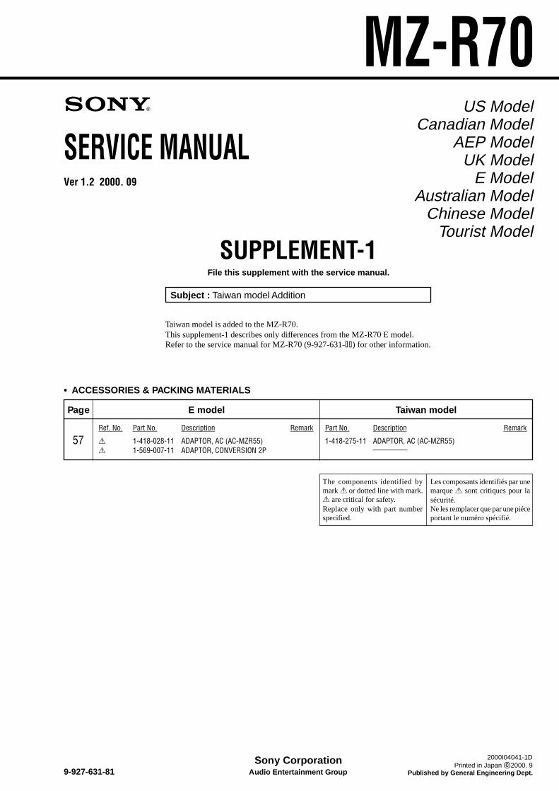
SERVICE MANUAL
Sony CorporationAudio Entertainment Group
2000I04041-1DPrinted in Japan C2000. 9
Published by General Engineering Dept.9-927-631-81
• ACCESSORIES & PACKING MATERIALS
Part No. Description Remark
Page E model Taiwan model
Ref. No. Part No. Description Remark
57 1-418-275-11 ADAPTOR, AC (AC-MZR55)0 1-418-028-11 ADAPTOR, AC (AC-MZR55)0 1-569-007-11 ADAPTOR, CONVERSION 2P
SUPPLEMENT-1File this supplement with the service manual.
Subject : Taiwan model Addition
Taiwan model is added to the MZ-R70.This supplement-1 describes only differences from the MZ-R70 E model.Refer to the service manual for MZ-R70 (9-927-631-S) for other information.
Ver 1.2 2000. 09
MZ-R70US Model
Canadian ModelAEP Model
UK ModelE Model
Australian ModelChinese Model
Tourist Model
The components identified bymark 0 or dotted line with mark.0 are critical for safety.Replace only with part numberspecified.
Les composants identifiés par unemarque 0 sont critiques pour lasécurité.Ne les remplacer que par une piéceportant le numéro spécifié.