MAX941MAX942 Hih-Speed Low-Power 3V5V Rail-to … 1.0 4.2 mW MAX942/MAX944 1.0 3.6 Propagation Delay...
12
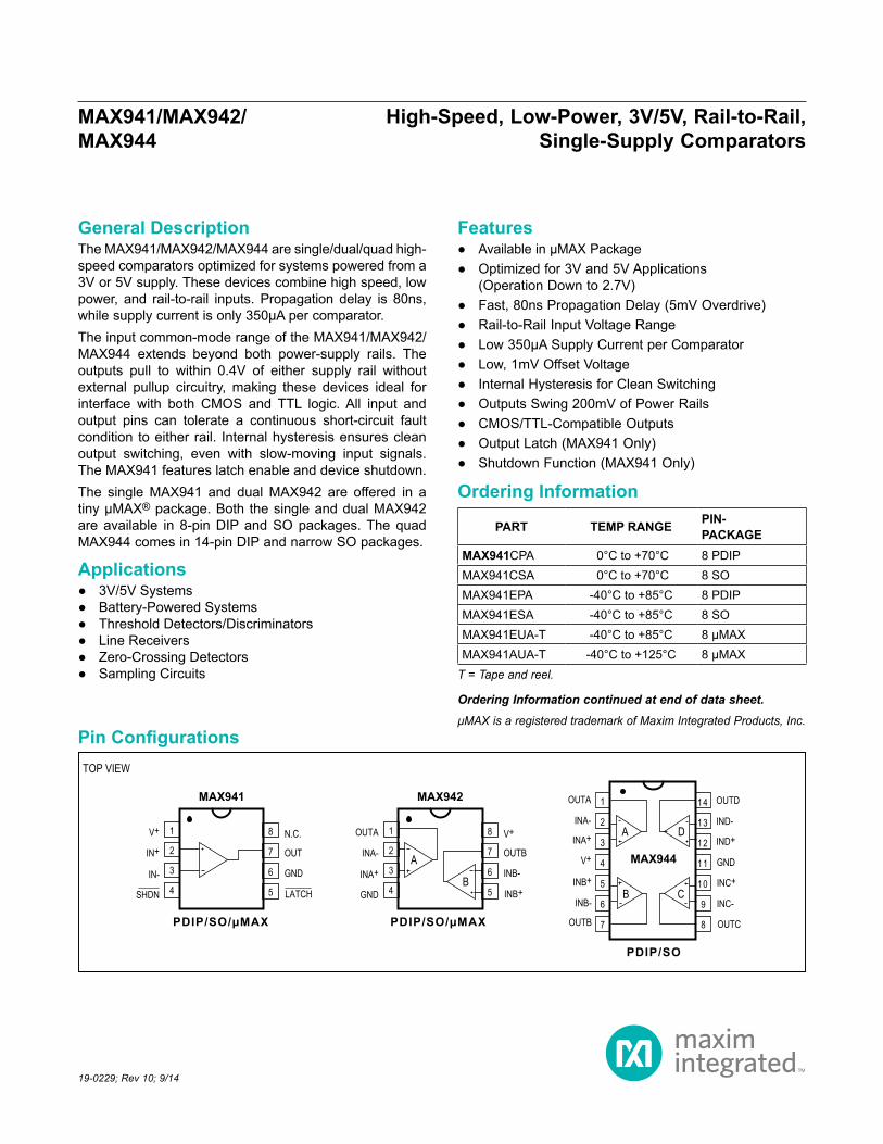
General Description The MAX941/MAX942/MAX944 are single/dual/quad high- speed comparators optimized for systems powered from a 3V or 5V supply. These devices combine high speed, low power, and rail-to-rail inputs. Propagation delay is 80ns, while supply current is only 350μA per comparator. The input common-mode range of the MAX941/MAX942/ MAX944 extends beyond both power-supply rails. The outputs pull to within 0.4V of either supply rail without external pullup circuitry, making these devices ideal for interface with both CMOS and TTL logic. All input and output pins can tolerate a continuous short-circuit fault condition to either rail. Internal hysteresis ensures clean output switching, even with slow-moving input signals. The MAX941 features latch enable and device shutdown. The single MAX941 and dual MAX942 are offered in a tiny μMAX ® package. Both the single and dual MAX942 are available in 8-pin DIP and SO packages. The quad MAX944 comes in 14-pin DIP and narrow SO packages. Applications ● 3V/5V Systems ● Battery-Powered Systems ● Threshold Detectors/Discriminators ● Line Receivers ● Zero-Crossing Detectors ● Sampling Circuits Features ● Available in μMAX Package ● Optimized for 3V and 5V Applications (Operation Down to 2.7V) ● Fast, 80ns Propagation Delay (5mV Overdrive) ● Rail-to-Rail Input Voltage Range ● Low 350μA Supply Current per Comparator ● Low, 1mV Offset Voltage ● Internal Hysteresis for Clean Switching ● Outputs Swing 200mV of Power Rails ● CMOS/TTL-Compatible Outputs ● Output Latch (MAX941 Only) ● Shutdown Function (MAX941 Only) Ordering Information continued at end of data sheet. μMAX is a registered trademark of Maxim Integrated Products, Inc. 19-0229; Rev 10; 9/14 T = Tape and reel. PART TEMP RANGE PIN- PACKAGE MAX941CPA 0°C to +70°C 8 PDIP MAX941CSA 0°C to +70°C 8 SO MAX941EPA -40°C to +85°C 8 PDIP MAX941ESA -40°C to +85°C 8 SO MAX941EUA-T -40°C to +85°C 8 µMAX MAX941AUA-T -40°C to +125°C 8 µMAX 1 2 3 4 8 7 6 5 N.C. OUT GND LATCH SHDN IN- IN + V + PDIP/SO/μMAX 1 2 3 4 8 7 6 5 V + OUTB INB- INB + GND INA + INA- OUTA MAX942 PDIP/SO/μMAX 14 13 12 11 10 9 8 1 2 3 4 5 6 7 OUTD IND- IND + GND V + INA + INA- OUTA INC + INC- OUTC OUTB INB- INB + PDIP/SO MAX941 MAX944 TOP VIEW A B A D B C MAX941/MAX942/ MAX944 High-Speed, Low-Power, 3V/5V, Rail-to-Rail, Single-Supply Comparators Pin Configurations Ordering Information
Transcript of MAX941MAX942 Hih-Speed Low-Power 3V5V Rail-to … 1.0 4.2 mW MAX942/MAX944 1.0 3.6 Propagation Delay...
General DescriptionThe MAX941/MAX942/MAX944 are single/dual/quad high-speed comparators optimized for systems powered from a 3V or 5V supply. These devices combine high speed, low power, and rail-to-rail inputs. Propagation delay is 80ns, while supply current is only 350μA per comparator.The input common-mode range of the MAX941/MAX942/MAX944 extends beyond both power-supply rails. The outputs pull to within 0.4V of either supply rail without external pullup circuitry, making these devices ideal for interface with both CMOS and TTL logic. All input and output pins can tolerate a continuous short-circuit fault condition to either rail. Internal hysteresis ensures clean output switching, even with slow-moving input signals. The MAX941 features latch enable and device shutdown.The single MAX941 and dual MAX942 are offered in a tiny μMAX® package. Both the single and dual MAX942 are available in 8-pin DIP and SO packages. The quad MAX944 comes in 14-pin DIP and narrow SO packages.
Applications 3V/5V Systems Battery-Powered Systems Threshold Detectors/Discriminators Line Receivers Zero-Crossing Detectors Sampling Circuits
Features Available in μMAX Package Optimized for 3V and 5V Applications
(Operation Down to 2.7V) Fast, 80ns Propagation Delay (5mV Overdrive) Rail-to-Rail Input Voltage Range Low 350μA Supply Current per Comparator Low, 1mV Offset Voltage Internal Hysteresis for Clean Switching Outputs Swing 200mV of Power Rails CMOS/TTL-Compatible Outputs Output Latch (MAX941 Only) Shutdown Function (MAX941 Only)
Ordering Information continued at end of data sheet.μMAX is a registered trademark of Maxim Integrated Products, Inc.
19-0229; Rev 10; 9/14
T = Tape and reel.
PART TEMP RANGE PIN-PACKAGE
MAX941CPA 0°C to +70°C 8 PDIPMAX941CSA 0°C to +70°C 8 SOMAX941EPA -40°C to +85°C 8 PDIPMAX941ESA -40°C to +85°C 8 SOMAX941EUA-T -40°C to +85°C 8 µMAXMAX941AUA-T -40°C to +125°C 8 µMAX
1
2
3
4
8
7
6
5
N.C.
OUT
GND
LATCHSHDN
IN-
IN+
V+
PDIP/SO/µMAX
1
2
3
4
8
7
6
5
V+
OUTB
INB-
INB+GND
INA+
INA-
OUTA
MAX942
PDIP/SO/µMAX
14
13
12
11
10
9
8
1
2
3
4
5
6
7
OUTD
IND-
IND+
GNDV+
INA+
INA-
OUTA
INC+
INC-
OUTCOUTB
INB-
INB+
PDIP/SO
MAX941
MAX944
TOP VIEW
A
B
A D
B C
MAX941/MAX942/ MAX944
High-Speed, Low-Power, 3V/5V, Rail-to-Rail, Single-Supply Comparators
Pin Configurations
Ordering Information
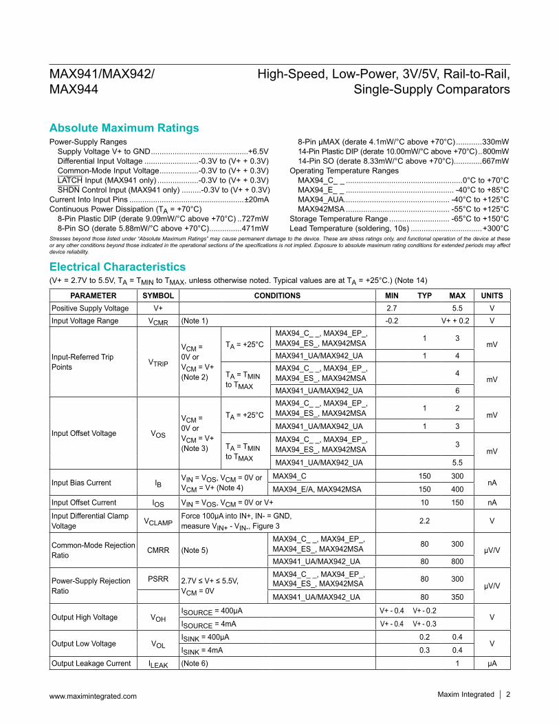
Power-Supply Ranges Supply Voltage V+ to GND .............................................+6.5V Differential Input Voltage .........................-0.3V to (V+ + 0.3V) Common-Mode Input Voltage ..................-0.3V to (V+ + 0.3V) LATCH Input (MAX941 only) ...................-0.3V to (V+ + 0.3V) SHDN Control Input (MAX941 only) .........-0.3V to (V+ + 0.3V)Current Into Input Pins .....................................................±20mAContinuous Power Dissipation (TA = +70°C) 8-Pin Plastic DIP (derate 9.09mW/°C above +70°C) ..727mW 8-Pin SO (derate 5.88mW/°C above +70°C) ...............471mW
8-Pin μMAX (derate 4.1mW/°C above +70°C) ............330mW 14-Pin Plastic DIP (derate 10.00mW/°C above +70°C) ..800mW 14-Pin SO (derate 8.33mW/°C above +70°C) .............667mWOperating Temperature Ranges MAX94_C_ _ ......................................................0°C to +70°C MAX94_E_ _ .................................................. -40°C to +85°C MAX94_AUA ................................................. -40°C to +125°C MAX942MSA ................................................ -55°C to +125°CStorage Temperature Range ............................ -65°C to +150°CLead Temperature (soldering, 10s) .................................+300°C
(V+ = 2.7V to 5.5V, TA = TMIN to TMAX, unless otherwise noted. Typical values are at TA = +25°C.) (Note 14)
PARAMETER SYMBOL CONDITIONS MIN TYP MAX UNITSPositive Supply Voltage V+ 2.7 5.5 VInput Voltage Range VCMR (Note 1) -0.2 V+ + 0.2 V
Input-Referred Trip Points VTRIP
VCM = 0V orVCM = V+(Note 2)
TA = +25°CMAX94_C_ _, MAX94_EP_,MAX94_ES_, MAX942MSA 1 3
mVMAX941_UA/MAX942_UA 1 4
TA = TMIN to TMAX
MAX94_C_ _, MAX94_EP_,MAX94_ES_, MAX942MSA 4
mVMAX941_UA/MAX942_UA 6
Input Offset Voltage VOS
VCM = 0V orVCM = V+(Note 3)
TA = +25°CMAX94_C_ _, MAX94_EP_,MAX94_ES_, MAX942MSA 1 2
mVMAX941_UA/MAX942_UA 1 3
TA = TMIN to TMAX
MAX94_C_ _, MAX94_EP_,MAX94_ES_, MAX942MSA 3
mVMAX941_UA/MAX942_UA 5.5
Input Bias Current IBVIN = VOS, VCM = 0V orVCM = V+ (Note 4)
MAX94_C 150 300nA
MAX94_E/A, MAX942MSA 150 400
Input Offset Current IOS VIN = VOS, VCM = 0V or V+ 10 150 nA
Input Differential Clamp Voltage VCLAMP
Force 100μA into IN+, IN- = GND, measure VIN+ - VIN-, Figure 3 2.2 V
Common-Mode Rejection Ratio CMRR (Note 5)
MAX94_C_ _, MAX94_EP_, MAX94_ES_, MAX942MSA 80 300
μV/VMAX941_UA/MAX942_UA 80 800
Power-Supply Rejection Ratio
PSRR 2.7V ≤ V+ ≤ 5.5V, VCM = 0V
MAX94_C_ _, MAX94_EP_, MAX94_ES_, MAX942MSA 80 300
μV/VMAX941_UA/MAX942_UA 80 350
Output High Voltage VOHISOURCE = 400μA V+ - 0.4 V+ - 0.2
VISOURCE = 4mA V+ - 0.4 V+ - 0.3
Output Low Voltage VOLISINK = 400μA 0.2 0.4
VISINK = 4mA 0.3 0.4
Output Leakage Current ILEAK (Note 6) 1 µA
MAX941/MAX942/ MAX944
High-Speed, Low-Power, 3V/5V, Rail-to-Rail, Single-Supply Comparators
www.maximintegrated.com Maxim Integrated 2
Absolute Maximum Ratings
Stresses beyond those listed under “Absolute Maximum Ratings” may cause permanent damage to the device. These are stress ratings only, and functional operation of the device at these or any other conditions beyond those indicated in the operational sections of the specifications is not implied. Exposure to absolute maximum rating conditions for extended periods may affect device reliability.
Electrical Characteristics
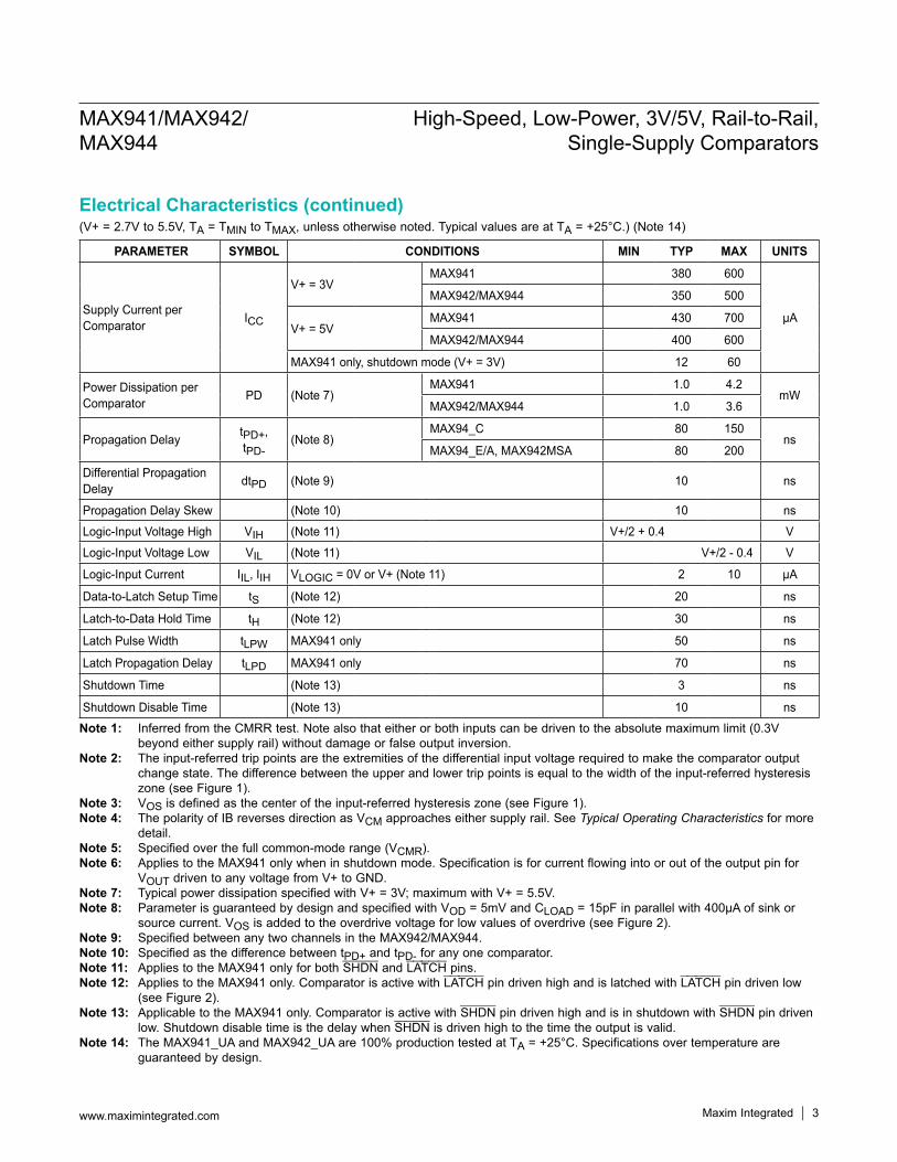
(V+ = 2.7V to 5.5V, TA = TMIN to TMAX, unless otherwise noted. Typical values are at TA = +25°C.) (Note 14)
Note 1: Inferred from the CMRR test. Note also that either or both inputs can be driven to the absolute maximum limit (0.3V beyond either supply rail) without damage or false output inversion.
Note 2: The input-referred trip points are the extremities of the differential input voltage required to make the comparator output change state. The difference between the upper and lower trip points is equal to the width of the input-referred hysteresis zone (see Figure 1).
Note 3: VOS is defined as the center of the input-referred hysteresis zone (see Figure 1).Note 4: The polarity of IB reverses direction as VCM approaches either supply rail. See Typical Operating Characteristics for more
detail.Note 5: Specified over the full common-mode range (VCMR).Note 6: Applies to the MAX941 only when in shutdown mode. Specification is for current flowing into or out of the output pin for
VOUT driven to any voltage from V+ to GND.Note 7: Typical power dissipation specified with V+ = 3V; maximum with V+ = 5.5V.Note 8: Parameter is guaranteed by design and specified with VOD = 5mV and CLOAD = 15pF in parallel with 400μA of sink or
source current. VOS is added to the overdrive voltage for low values of overdrive (see Figure 2).Note 9: Specified between any two channels in the MAX942/MAX944.Note 10: Specified as the difference between tPD+ and tPD- for any one comparator.Note 11: Applies to the MAX941 only for both SHDN and LATCH pins.Note 12: Applies to the MAX941 only. Comparator is active with LATCH pin driven high and is latched with LATCH pin driven low
(see Figure 2).Note 13: Applicable to the MAX941 only. Comparator is active with SHDN pin driven high and is in shutdown with SHDN pin driven
low. Shutdown disable time is the delay when SHDN is driven high to the time the output is valid.Note 14: The MAX941_UA and MAX942_UA are 100% production tested at TA = +25°C. Specifications over temperature are
guaranteed by design.
PARAMETER SYMBOL CONDITIONS MIN TYP MAX UNITS
Supply Current per Comparator ICC
V+ = 3VMAX941 380 600
μA
MAX942/MAX944 350 500
V+ = 5VMAX941 430 700
MAX942/MAX944 400 600
MAX941 only, shutdown mode (V+ = 3V) 12 60
Power Dissipation per Comparator PD (Note 7)
MAX941 1.0 4.2mW
MAX942/MAX944 1.0 3.6
Propagation Delay tPD+,tPD-
(Note 8)MAX94_C 80 150
nsMAX94_E/A, MAX942MSA 80 200
Differential Propagation Delay dtPD (Note 9) 10 ns
Propagation Delay Skew (Note 10) 10 ns
Logic-Input Voltage High VIH (Note 11) V+/2 + 0.4 V
Logic-Input Voltage Low VIL (Note 11) V+/2 - 0.4 V
Logic-Input Current IIL, IIH VLOGIC = 0V or V+ (Note 11) 2 10 µA
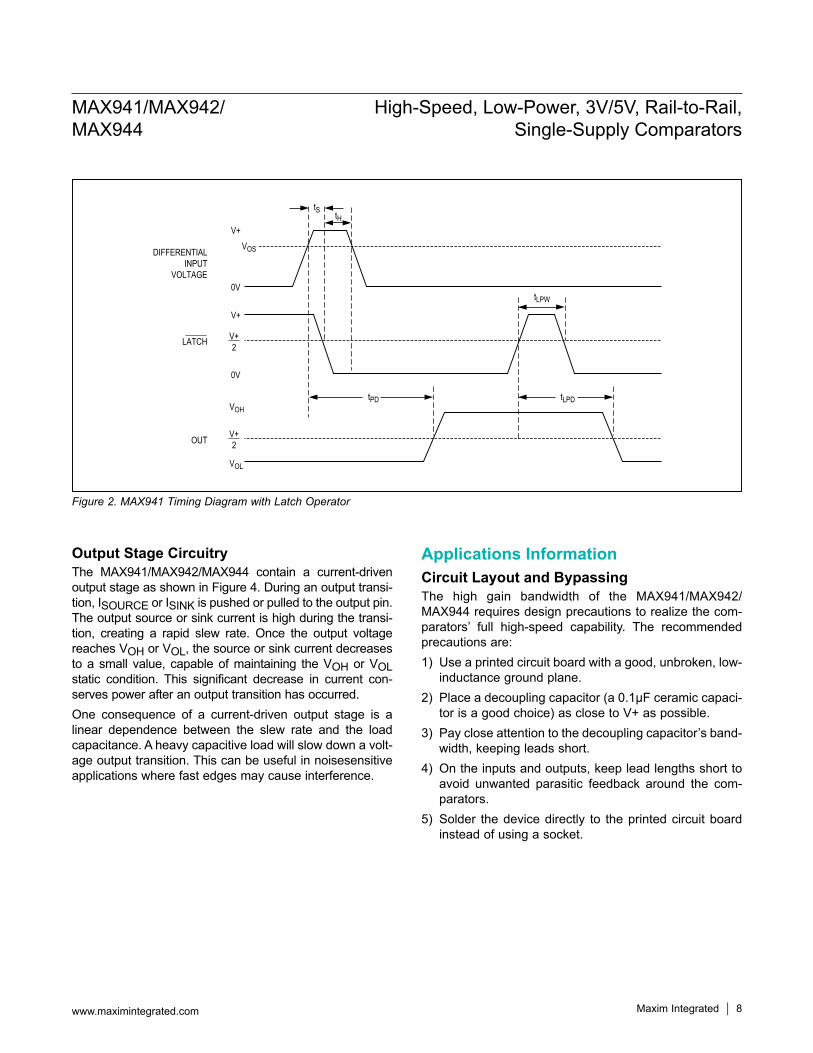
Data-to-Latch Setup Time tS (Note 12) 20 ns
Latch-to-Data Hold Time tH (Note 12) 30 ns
Latch Pulse Width tLPW MAX941 only 50 ns
Latch Propagation Delay tLPD MAX941 only 70 ns
Shutdown Time (Note 13) 3 ns
Shutdown Disable Time (Note 13) 10 ns
MAX941/MAX942/ MAX944
High-Speed, Low-Power, 3V/5V, Rail-to-Rail, Single-Supply Comparators
www.maximintegrated.com Maxim Integrated 3
Electrical Characteristics (continued)
(V+ = 3.0V, TA = +25°C, unless otherwise noted.)
100
40
0 100
PROPAGATION DELAY vs. INPUT OVERDRIVE
50
90 MAX9
41 to
c01
INPUT OVERDRIVE (mV)
PROP
AGAT
ION
DELA
Y (n
s)
75
70
60
25 50
80
30
tPD+
tPD-
RS = 10ΩCLOAD = 15pF
130
-60 -20 40 80
PROPAGATION DELAY vs.TEMPERATURE
70
110
MAX9
41 to
c04
TEMPERATURE (°C)
PROP
AGAT
ION
DELA
Y (n
s)
0 60
90
120
60
100
80
-40 20 100 120 140
RS = 10ΩCLOAD = 15pFVOD = 5mV
01
OUTPUT LOW VOLTAGEvs. SINK CURRENT
MAX9
41 to
c07
SINK CURRENT (µA)
V OL (
V)
0.1
0.2
0.3
0.4
0.5
10 100 1000 10,000
TA = -55°C
TA = +25°C
TA = +125°C
400
100
10 100k
PROPAGATION DELAY vs. SOURCE IMPEDANCE
150
350 MAX9
41 to
c02
SOURCE IMPEDANCE (Ω)
PROP
AGAT
ION
DELA
Y (n
s)
10k
250
200
100 1k
300
50
tPD+
tPD-
CLOAD = 15pFVOD = 5mV
100
40
2 6
PROPAGATION DELAY vs. SUPPLY VOLTAGE
50
90 MAX9
41 to
c05
SUPPLY VOLTAGE (V)
PROP
AGAT
ION
DELA
Y (n
s)
5
70
60
3 4
80
30
tPD+
tPD-
RS = 10ΩCLOAD = 15pFVOD = 5mV
MAX941 TOTAL SUPPLY CURRENTvs. SUPPLY VOLTAGE
SUPP
LY C
URRE
NT (µ
A)
02
SUPPLY VOLTAGE (V)
100
200
300
400
500
600
3 4 5 6
MAX9
41 to
c08
TA = +125°C
TA = +25°C
TA = -55°C
180
600
PROPAGATION DELAY vs. CAPACITIVE LOAD
80
160 MAX9
41 to
c03
CAPACITIVE LOAD (pF)
PROP
AGAT
ION
DELA
Y (n
s)
400
120
100
100 300 500
140
200
RS = 10ΩVOD = 5mV
tPD+
tPD-
2.6
1 10,000
OUTPUT HIGH VOLTAGE vs. SOURCE CURRENT
2.7
MAX9
41 to
c06
SOURCE CURRENT (µA)
V OH
(V)
1000
2.9
2.8
10 100
3.0
2.5
TA = +125°C
TA = +25°C
TA = -55°C
MAX942 TOTAL SUPPLY CURRENTvs. SUPPLY VOLTAGE
SUPP
LY C
URRE
NT (µ
A)
300
SUPPLY VOLTAGE (V)
400
500
600
700
800
MAX9
41 to
c09
TA = +125°C
TA = +25°C
TA = -55°C
2 3 4 5 6
MAX941/MAX942/ MAX944
High-Speed, Low-Power, 3V/5V, Rail-to-Rail, Single-Supply Comparators
Maxim Integrated 4www.maximintegrated.com
Typical Operating Characteristics
(V+ = 3.0V, TA = +25°C, unless otherwise noted.)
MAX944 TOTAL SUPPLY CURRENTvs. SUPPLY VOLTAGE
SUPP
LY C
URRE
NT (m
A)
0.75
SUPPLY VOLTAGE (V)
1.00
1.25
1.50
1.75
2.00
MAX9
41 to
c10
TA = +25°C
TA = -55°C
2 3 4 5 6
TA = +125°C
VOLTAGE TRIP POINTS/INPUT OFFSET VOLTAGE vs. TEMPERATURE
TRIP
POI
NTS
/ VOS
(µV)
TEMPERATURE (°C)
-2000
-1500
-500
0
1000
-1000
MAX9
41 to
c13
-60 140-40 -20 0 20 40 60 80 100 120
500VTRIP+
VTRIP-
VOS
VCM = 0
MAX941 SHUTDOWN SUPPLY CURRENTvs. TEMPERATURE
SHUT
DOW
N SU
PPLY
CUR
RENT
(µA)
0
10
20
30
40
TEMPERATURE (°C)
MAX9
41 to
c16
-60 -40 -20 0 20 40 60 80 100 120 140
V+ = 6.0V
V+ = 2.7V
10MHz RESPONSE
INPUT50mV/div
OUTPUT1V/div
VOS
V+
GND
50ns/div
MAX941 toc17
INPUT VOLTAGE RANGEvs. TEMPERATURE
INPU
T VO
LTAG
E RA
NGE
(V)
TEMPERATURE (°C)
-1
0
2
3
4
1
-60 140-40 -20 0 20 40 60 80 100 120
MAX9
41 to
c11
VCM+
V+ = 3.0V
VCM-
INPUT BIAS CURRENT/INPUT OFFSET CURRENT vs. TEMPERATURE
INPU
T BI
AS / O
FFSE
T CU
RREN
T (n
A)
TEMPERATURE (°C)
0
50
150
200
250
100
MAX9
41-1
4
-60 140-40 -20 0 20 40 60 80 100 120
IB+
IB-
IOS
SHORT-CIRCUIT OUTPUT CURRENTvs. TEMPERATURE
SHOR
T-CI
RCUI
T OUT
PUT C
URRE
NT (m
A)
0
10
20
30
40
TEMPERATURE (°C)
MAX9
41 to
c12
-60 -40 -20 0 20 40 60 80 100 120 140
OUTPUT SHORTEDTO V+ (SINKING)
OUTPUT SHORTEDTO GND (SOURCING)
INPUT BIAS CURRENT (IB+, IB-) vs. COMMON-MODE VOLTAGE
I B+, I B
- (nA
)
-100
COMMON-MODE VOLTAGE (V)
MAX9
41 to
c15
-50
0
50
100
150
200
250
0 1 2 3 4 5 6
TA = -55°C
TA = +25°C
TA = +125°C
VIN+ = VIN-NEGATIVE VALUESREPRESENT CURRENTFLOWING INTO THE DEVICE
V+ = 6V
MAX941/MAX942/ MAX944
High-Speed, Low-Power, 3V/5V, Rail-to-Rail, Single-Supply Comparators
Maxim Integrated 5www.maximintegrated.com
Typical Operating Characteristics (continued)
(V+ = 3.0V, TA = +25°C, unless otherwise noted.)
PINNAME FUNCTION
MAX941 MAX942 MAX944— 1 1 OUTA Comparator A Output
— 2 2 INA- Comparator A Inverting Input
— 3 3 INA+ Comparator A Noninverting Input
1 8 4 V+ Positive Supply (V+ to GND must be ≤ 6.5V)
— 5 5 INB+ Comparator B Noninverting Input
— 6 6 INB- Comparator B Inverting Input
— 7 7 OUTB Comparator B Output
— — 8 OUTC Comparator C Output
— — 9 INC- Comparator C Inverting Input
— — 10 INC+ Comparator C Noninverting Input
6 4 11 GND Ground
— — 12 IND+ Comparator D Noninverting Input
— — 13 IND- Comparator D Inverting Input
— — 14 OUTD Comparator D Output
2 — — IN+ Noninverting Input
3 — — IN- Inverting Input
4 — — SHDN Shutdown: MAX941 is active when SHDN is driven high; MAX941 is in shutdown when SHDN is driven low.
5 — — LATCH The output is latched when LATCH is low. The latch is transparent when LATCH is high.
7 — — OUT Comparator Output
8 — — N.C. No Connection. Not internally connected.
PROPAGATION DELAY (tPD+)
INPUT STEP = 100mVVOD = +5mV
INPUT50mV/div
OUTPUT1V/div
VODVOS
V+
V+2
GND
20ns/divtPD+
MAX941 toc18PROPAGATION DELAY (tPD-)
INPUT STEP = 100mVVOD = -5mV
INPUT50mV/div
OUTPUT1V/div
VODVOS
V+
V+2
GND
20ns/divtPD-
MAX941 toc19
MAX941/MAX942/ MAX944
High-Speed, Low-Power, 3V/5V, Rail-to-Rail, Single-Supply Comparators
www.maximintegrated.com Maxim Integrated 6
Pin Description
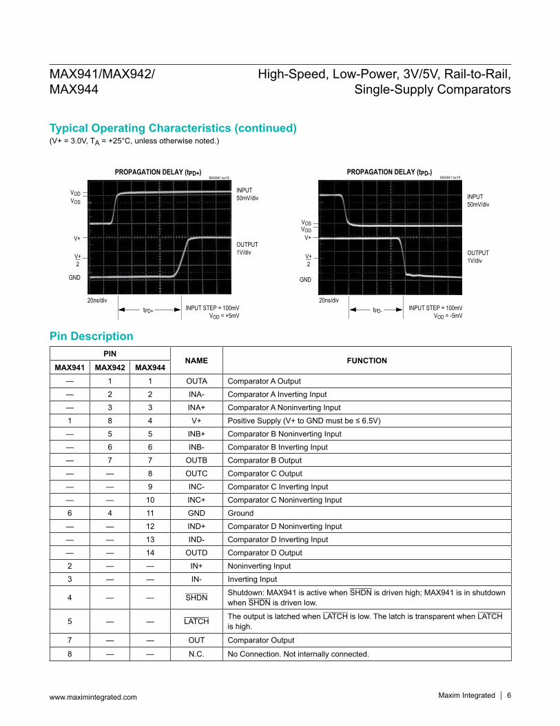
Typical Operating Characteristics (continued)
Detailed DescriptionThe MAX941/MAX942/MAX944 single-supply compara-tors feature internal hysteresis, high speed, and low power. Their outputs are guaranteed to pull within 0.4V of either supply rail without external pullup or pulldown circuitry. Rail-to-rail input voltage range and low-voltage single-supply operation make these devices ideal for por-table equipment. The MAX941/MAX942/MAX944 inter-face directly to CMOS and TTL logic.
TimingMost high-speed comparators oscillate in the linear region because of noise or undesired parasitic feedback. This tends to occur when the voltage on one input is at or equal to the voltage on the other input. To counter the parasitic effects and noise, the MAX941/MAX942/MAX944 have internal hysteresis.The hysteresis in a comparator creates two trip points: one for the rising input voltage and one for the falling input voltage (Figure 1). The difference between the trip points is the hysteresis. When the comparator’s input voltages are equal, the hysteresis effectively causes one com-parator input voltage to move quickly past the other, thus taking the input out of the region where oscillation occurs. Standard comparators require hysteresis to be added with external resistors. The MAX941/MAX942/MAX944’s
fixed internal hysteresis eliminates these resistors and the equations needed to determine appropriate values.Figure 1 illustrates the case where IN- is fixed and IN+ is varied. If the inputs were reversed, the figure would look the same, except the output would be inverted.The MAX941 includes an internal latch that allows stor-age of comparison results. The LATCH pin has a high input impedance. If LATCH is high, the latch is transpar-ent (i.e., the comparator operates as though the latch is not present). The comparator’s output state is stored when LATCH is pulled low. All timing constraints must be met when using the latch function (Figure 2).
Shutdown Mode (MAX941 Only)The MAX941 shuts down when SHDN is low. When shut down, the supply current drops to less than 60μA, and the three-state output becomes high impedance. The SHDN pin has a high input impedance. Connect SHDN to V+ for normal operation. Exit shutdown with LATCH high; other-wise, the output will be indeterminate.
Input Stage CircuitryThe MAX941/MAX942/MAX944 include internal protec-tion circuitry that prevents damage to the precision input stage from large differential input voltages. This protection circuitry consists of two back-to-back diodes between IN+ and IN- as well as two 4.1kΩ resistors (Figure 3). The diodes limit the differential voltage applied to the internal circuitry of the comparators to be no more than 2VF, where VF is the forward voltage drop of the diode (about 0.7V at +25°C).For a large differential input voltage (exceeding 2VF), this protection circuitry increases the input bias current at IN+ (source) and IN- (sink).
F(IN IN ) 2VInput Current 2 x 4.1k+ − − −
=Ω
Input current with large differential input voltages should not be confused with input bias current (IB). As long as the differential input voltage is less than 2VF, this input cur-rent is equal to IB. The protection circuitry also allows for the input common-mode range of the MAX941/MAX942/MAX944 to extend beyond both power-supply rails. The output is in the correct logic state if one or both inputs are within the common-mode range.
Figure 1. Input and Output Waveform, Noninverting Input Varied
VTRIP+
VHYST
VTRIP-
COMPARATOROUTPUT
VOH
VOL
VTRIP+ + VTRIP-2
VOS =
VIN- = 0V
VIN+
MAX941/MAX942/ MAX944
High-Speed, Low-Power, 3V/5V, Rail-to-Rail, Single-Supply Comparators
www.maximintegrated.com Maxim Integrated 7
Output Stage CircuitryThe MAX941/MAX942/MAX944 contain a current-driven output stage as shown in Figure 4. During an output transi-tion, ISOURCE or ISINK is pushed or pulled to the output pin. The output source or sink current is high during the transi-tion, creating a rapid slew rate. Once the output voltage reaches VOH or VOL, the source or sink current decreases to a small value, capable of maintaining the VOH or VOL static condition. This significant decrease in current con-serves power after an output transition has occurred.One consequence of a current-driven output stage is a linear dependence between the slew rate and the load capacitance. A heavy capacitive load will slow down a volt-age output transition. This can be useful in noisesensitive applications where fast edges may cause interference.
Applications InformationCircuit Layout and BypassingThe high gain bandwidth of the MAX941/MAX942/ MAX944 requires design precautions to realize the com-parators’ full high-speed capability. The recommended precautions are:1) Use a printed circuit board with a good, unbroken, low-
inductance ground plane.2) Place a decoupling capacitor (a 0.1μF ceramic capaci-
tor is a good choice) as close to V+ as possible.3) Pay close attention to the decoupling capacitor’s band-
width, keeping leads short.4) On the inputs and outputs, keep lead lengths short to
avoid unwanted parasitic feedback around the com-parators.
5) Solder the device directly to the printed circuit board instead of using a socket.
Figure 2. MAX941 Timing Diagram with Latch Operator
VOH
tLPW
OUT
tLPDtPD
V+
0V
V+
0V
V+2
V+2
VOL
LATCH
DIFFERENTIALINPUT
VOLTAGE
VOS
tHtS
MAX941/MAX942/ MAX944
High-Speed, Low-Power, 3V/5V, Rail-to-Rail, Single-Supply Comparators
www.maximintegrated.com Maxim Integrated 8
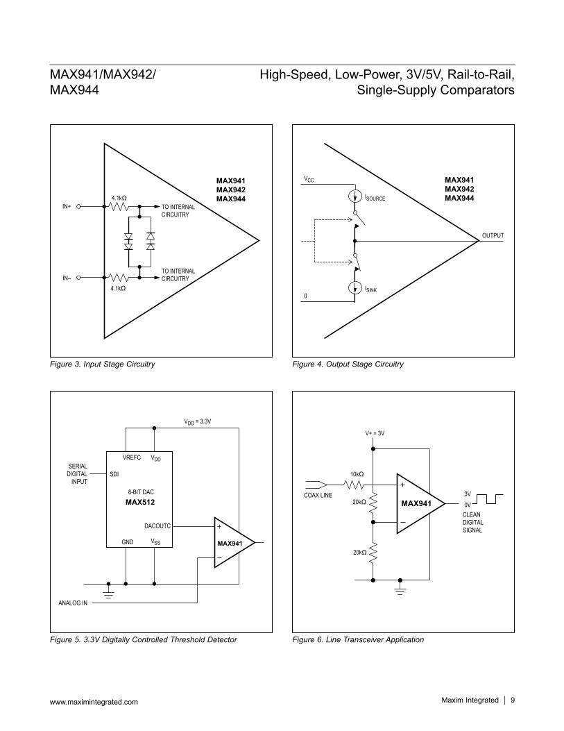
Figure 3. Input Stage Circuitry
Figure 5. 3.3V Digitally Controlled Threshold Detector
Figure 4. Output Stage Circuitry
Figure 6. Line Transceiver Application
MAX941MAX942MAX944
4.1kΩ
4.1kΩ
TO INTERNALCIRCUITRY
TO INTERNALCIRCUITRY
IN–
IN+ISOURCE
ISINK
VCC
0
OUTPUT
MAX941MAX942MAX944
ANALOG IN
VSS
SERIALDIGITAL
INPUT
MAX512
VDD
SDI
DACOUTC
VDD = 3.3V
VREFC
8-BIT DAC
GND MAX941
0V3V
CLEANDIGITALSIGNAL
10kΩ
20kΩ
20kΩ
V+ = 3V
COAX LINEMAX941
MAX941/MAX942/ MAX944
High-Speed, Low-Power, 3V/5V, Rail-to-Rail, Single-Supply Comparators
www.maximintegrated.com Maxim Integrated 9
T = Tape and reel.
PART TEMP RANGE PIN-PACKAGE
MAX942MSA/PR -55°C to +125°C 8 SO
MAX942CPA 0°C to +70°C 8 PDIP
MAX942CSA 0°C to +70°C 8 SO
MAX942EPA -40°C to +85°C 8 PDIP
MAX942ESA -40°C to +85°C 8 SO
MAX942EUA-T -40°C to +85°C 8 µMAX
MAX942AUA-T -40°C to +125°C 8 µMAX
MAX944CPD 0°C to +70°C 14 PDIP
MAX944CSD 0°C to +70°C 14 SO
MAX944EPD -40°C to +85°C 14 PDIP
MAX944ESD -40°C to +85°C 14 SO
MAX941/MAX942/ MAX944
High-Speed, Low-Power, 3V/5V, Rail-to-Rail, Single-Supply Comparators
www.maximintegrated.com Maxim Integrated 10
Chip InformationPROCESS: BIPOLAR
Ordering Information (continued)
PACKAGE TYPE PACKAGE CODE OUTLINE NO. LAND PATTERN NO.
8 μMAX U8-1 21-0036 90-0092
8 PDIP P8-1 21-0043 —
8 SO S8-2 21-0041 90-0096
14 PDIP P14-3 21-0043 —
14 SO S14-1 21-0041 90-0112
MAX941/MAX942/ MAX944
High-Speed, Low-Power, 3V/5V, Rail-to-Rail, Single-Supply Comparators
www.maximintegrated.com Maxim Integrated 11
Package InformationFor the latest package outline information and land patterns (footprints), go to www.maximintegrated.com/packages. Note that a “+”, “#”, or “-” in the package code indicates RoHS status only. Package drawings may show a different suffix character, but the drawing pertains to the package regardless of RoHS status.
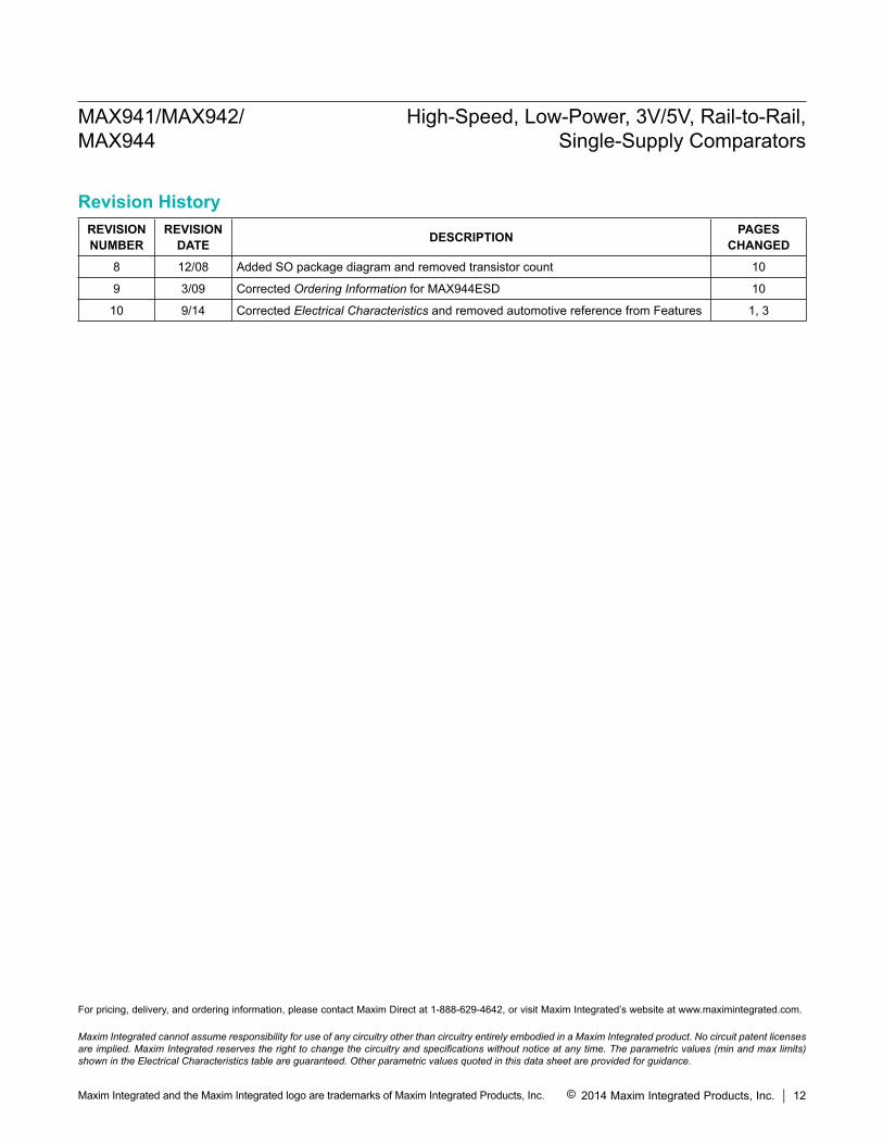
REVISIONNUMBER
REVISIONDATE DESCRIPTION PAGES
CHANGED
8 12/08 Added SO package diagram and removed transistor count 10
9 3/09 Corrected Ordering Information for MAX944ESD 10
10 9/14 Corrected Electrical Characteristics and removed automotive reference from Features 1, 3
Maxim Integrated cannot assume responsibility for use of any circuitry other than circuitry entirely embodied in a Maxim Integrated product. No circuit patent licenses are implied. Maxim Integrated reserves the right to change the circuitry and specifications without notice at any time. The parametric values (min and max limits) shown in the Electrical Characteristics table are guaranteed. Other parametric values quoted in this data sheet are provided for guidance.
Maxim Integrated and the Maxim Integrated logo are trademarks of Maxim Integrated Products, Inc.
MAX941/MAX942/ MAX944
High-Speed, Low-Power, 3V/5V, Rail-to-Rail, Single-Supply Comparators
© 2014 Maxim Integrated Products, Inc. 12
Revision History
For pricing, delivery, and ordering information, please contact Maxim Direct at 1-888-629-4642, or visit Maxim Integrated’s website at www.maximintegrated.com.