LTC3633 - datasheet.octopart.com€¦ · n 3.6V to 15V Input Voltage Range ... RT ITH1 ITH2 INTVCC...
28
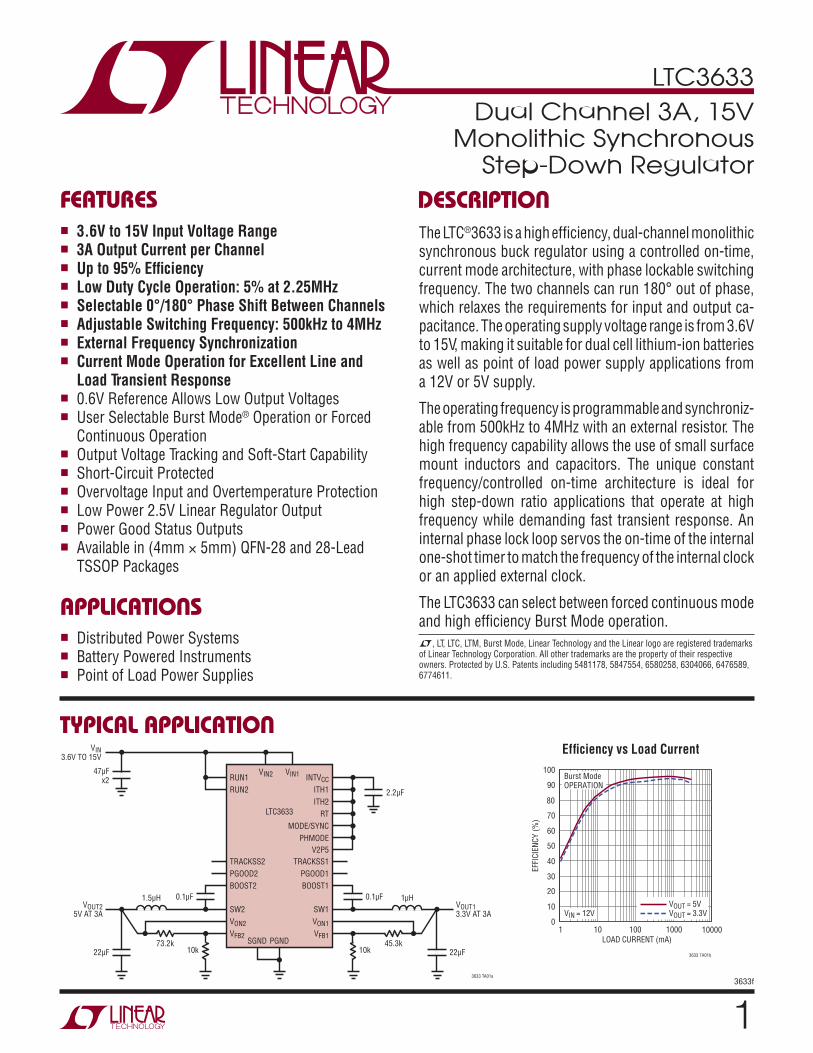
LTC3633 1 3633f n 3.6V to 15V Input Voltage Range n 3A Output Current per Channel n Up to 95% Efficiency n Low Duty Cycle Operation: 5% at 2.25MHz n Selectable 0°/180° Phase Shift Between Channels n Adjustable Switching Frequency: 500kHz to 4MHz n External Frequency Synchronization n Current Mode Operation for Excellent Line and Load Transient Response n 0.6V Reference Allows Low Output Voltages n User Selectable Burst Mode ® Operation or Forced Continuous Operation n Output Voltage Tracking and Soft-Start Capability n Short-Circuit Protected n Overvoltage Input and Overtemperature Protection n Low Power 2.5V Linear Regulator Output n Power Good Status Outputs n Available in (4mm × 5mm) QFN-28 and 28-Lead TSSOP Packages TYPICAL APPLICATION DESCRIPTION Dual Channel 3A, 15V Monolithic Synchronous Step-Down Regulator The LTC ® 3633 is a high efficiency, dual-channel monolithic synchronous buck regulator using a controlled on-time, current mode architecture, with phase lockable switching frequency. The two channels can run 180° out of phase, which relaxes the requirements for input and output ca- pacitance. The operating supply voltage range is from 3.6V to 15V, making it suitable for dual cell lithium-ion batteries as well as point of load power supply applications from a 12V or 5V supply. The operating frequency is programmable and synchroniz- able from 500kHz to 4MHz with an external resistor. The high frequency capability allows the use of small surface mount inductors and capacitors. The unique constant frequency/controlled on-time architecture is ideal for high step-down ratio applications that operate at high frequency while demanding fast transient response. An internal phase lock loop servos the on-time of the internal one-shot timer to match the frequency of the internal clock or an applied external clock. The LTC3633 can select between forced continuous mode and high efficiency Burst Mode operation. FEATURES APPLICATIONS n Distributed Power Systems n Battery Powered Instruments n Point of Load Power Supplies Efficiency vs Load Current L, LT, LTC, LTM, Burst Mode, Linear Technology and the Linear logo are registered trademarks of Linear Technology Corporation. All other trademarks are the property of their respective owners. Protected by U.S. Patents including 5481178, 5847554, 6580258, 6304066, 6476589, 6774611. 1 0 EFFICIENCY (%) 10 30 40 50 70 100 10000 3633 TA01b 20 80 100 90 60 10 1000 V OUT = 5V V OUT = 3.3V LOAD CURRENT (mA) Burst Mode OPERATION V IN = 12V RUN1 RUN2 TRACKSS2 PGOOD2 LTC3633 BOOST2 0.1μF 1.5μH 73.2k 10k SW2 V ON2 V IN2 PGND SGND V IN1 V FB2 PHMODE TRACKSS1 PGOOD1 BOOST1 SW1 V ON1 V FB1 22μF V OUT2 5V AT 3A 0.1μF 1μH 45.3k 10k 22μF V OUT1 3.3V AT 3A V IN 3.6V TO 15V 47μF x2 MODE/SYNC V2P5 RT ITH1 ITH2 INTV CC 2.2μF 3633 TA01a
Transcript of LTC3633 - datasheet.octopart.com€¦ · n 3.6V to 15V Input Voltage Range ... RT ITH1 ITH2 INTVCC...
LTC3633
13633f
n 3.6V to 15V Input Voltage Rangen 3A Output Current per Channeln Up to 95% Effi ciencyn Low Duty Cycle Operation: 5% at 2.25MHzn Selectable 0°/180° Phase Shift Between Channelsn Adjustable Switching Frequency: 500kHz to 4MHzn External Frequency Synchronizationn Current Mode Operation for Excellent Line and
Load Transient Responsen 0.6V Reference Allows Low Output Voltagesn User Selectable Burst Mode® Operation or Forced
Continuous Operationn Output Voltage Tracking and Soft-Start Capabilityn Short-Circuit Protectedn Overvoltage Input and Overtemperature Protectionn Low Power 2.5V Linear Regulator Outputn Power Good Status Outputsn Available in (4mm × 5mm) QFN-28 and 28-Lead
TSSOP Packages
TYPICAL APPLICATION
DESCRIPTION
Dual Channel 3A, 15V Monolithic Synchronous
Step-Down Regulator
The LTC®3633 is a high effi ciency, dual-channel monolithic synchronous buck regulator using a controlled on-time, current mode architecture, with phase lockable switching frequency. The two channels can run 180° out of phase, which relaxes the requirements for input and output ca-pacitance. The operating supply voltage range is from 3.6V to 15V, making it suitable for dual cell lithium-ion batteries as well as point of load power supply applications from a 12V or 5V supply.
The operating frequency is programmable and synchroniz-able from 500kHz to 4MHz with an external resistor. The high frequency capability allows the use of small surface mount inductors and capacitors. The unique constant frequency/controlled on-time architecture is ideal for high step-down ratio applications that operate at high frequency while demanding fast transient response. An internal phase lock loop servos the on-time of the internal one-shot timer to match the frequency of the internal clock or an applied external clock.
The LTC3633 can select between forced continuous mode and high effi ciency Burst Mode operation.
FEATURES
APPLICATIONSn Distributed Power Systemsn Battery Powered Instrumentsn Point of Load Power Supplies
Effi ciency vs Load Current
L, LT, LTC, LTM, Burst Mode, Linear Technology and the Linear logo are registered trademarks of Linear Technology Corporation. All other trademarks are the property of their respective owners. Protected by U.S. Patents including 5481178, 5847554, 6580258, 6304066, 6476589, 6774611.
10
EFF
ICIE
NC
Y (
%)
10
30
40
50
70
100 10000
3633 TA01b
20
80
100
90
60
10 1000
VOUT = 5VVOUT = 3.3V
LOAD CURRENT (mA)
Burst ModeOPERATION
VIN = 12V
RUN1
RUN2
TRACKSS2
PGOOD2
LTC3633
BOOST2
0.1μF1.5μH
73.2k10k
SW2
VON2
VIN2
PGNDSGND
VIN1
VFB2
PHMODE
TRACKSS1
PGOOD1
BOOST1
SW1
VON1
VFB1
22μF
VOUT2 5V AT 3A
0.1μF 1μH
45.3k10k 22μF
VOUT13.3V AT 3A
VIN 3.6V TO 15V
47μFx2
MODE/SYNC
V2P5
RT
ITH1
ITH2
INTVCC
2.2μF
3633 TA01a
LTC3633
23633f
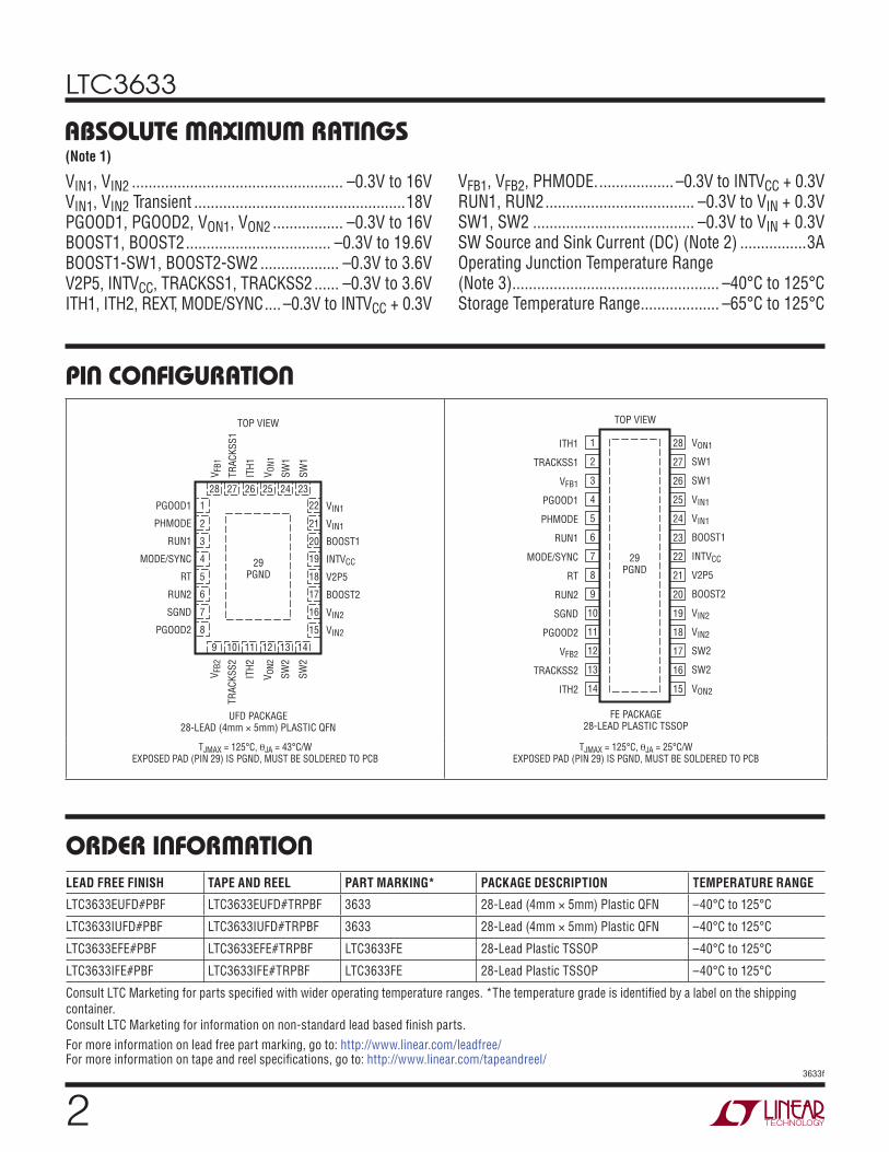
PIN CONFIGURATION
ABSOLUTE MAXIMUM RATINGS
VIN1, VIN2 ................................................... –0.3V to 16VVIN1, VIN2 Transient ...................................................18VPGOOD1, PGOOD2, VON1, VON2 ................. –0.3V to 16VBOOST1, BOOST2 ................................... –0.3V to 19.6VBOOST1-SW1, BOOST2-SW2 ................... –0.3V to 3.6VV2P5, INTVCC, TRACKSS1, TRACKSS2 ...... –0.3V to 3.6VITH1, ITH2, REXT, MODE/SYNC .... –0.3V to INTVCC + 0.3V
(Note 1)
ORDER INFORMATIONLEAD FREE FINISH TAPE AND REEL PART MARKING* PACKAGE DESCRIPTION TEMPERATURE RANGE
LTC3633EUFD#PBF LTC3633EUFD#TRPBF 3633 28-Lead (4mm × 5mm) Plastic QFN –40°C to 125°C
LTC3633IUFD#PBF LTC3633IUFD#TRPBF 3633 28-Lead (4mm × 5mm) Plastic QFN –40°C to 125°C
LTC3633EFE#PBF LTC3633EFE#TRPBF LTC3633FE 28-Lead Plastic TSSOP –40°C to 125°C
LTC3633IFE#PBF LTC3633IFE#TRPBF LTC3633FE 28-Lead Plastic TSSOP –40°C to 125°C
Consult LTC Marketing for parts specifi ed with wider operating temperature ranges. *The temperature grade is identifi ed by a label on the shipping
container.
Consult LTC Marketing for information on non-standard lead based fi nish parts.
For more information on lead free part marking, go to: http://www.linear.com/leadfree/ For more information on tape and reel specifi cations, go to: http://www.linear.com/tapeandreel/
VFB1, VFB2, PHMODE. .................. –0.3V to INTVCC + 0.3VRUN1, RUN2 .................................... –0.3V to VIN + 0.3VSW1, SW2 ....................................... –0.3V to VIN + 0.3VSW Source and Sink Current (DC) (Note 2) ................3AOperating Junction Temperature Range (Note 3) .................................................. –40°C to 125°CStorage Temperature Range ................... –65°C to 125°C
9 10
TOP VIEW
UFD PACKAGE28-LEAD (4mm × 5mm) PLASTIC QFN
11 12 13
28 27 26 25 24
14
23
6
5
4
3
2
1PGOOD1
PHMODE
RUN1
MODE/SYNC
RT
RUN2
SGND
PGOOD2
VIN1
VIN1
BOOST1
INTVCC
V2P5
BOOST2
VIN2
VIN2
VFB
1
TR
AC
KS
S1
ITH
1
VO
N1
SW
1
SW
1
VFB
2
TR
AC
KS
S2
ITH
2
VO
N2
SW
2
SW
2
7
17
18
19
20
21
22
16
8 15
29PGND
1
2
3
4
5
6
7
8
9
10
11
12
13
14
TOP VIEW
FE PACKAGE28-LEAD PLASTIC TSSOP
28
27
26
25
24
23
22
21
20
19
18
17
16
15
ITH1
TRACKSS1
VFB1
PGOOD1
PHMODE
RUN1
MODE/SYNC
RT
RUN2
SGND
PGOOD2
VFB2
TRACKSS2
ITH2
VON1
SW1
SW1
VIN1
VIN1
BOOST1
INTVCC
V2P5
BOOST2
VIN2
VIN2
SW2
SW2
VON2
29PGND
TJMAX = 125°C, θJA = 43°C/WEXPOSED PAD (PIN 29) IS PGND, MUST BE SOLDERED TO PCB
TJMAX = 125°C, θJA = 25°C/WEXPOSED PAD (PIN 29) IS PGND, MUST BE SOLDERED TO PCB
LTC3633
33633f
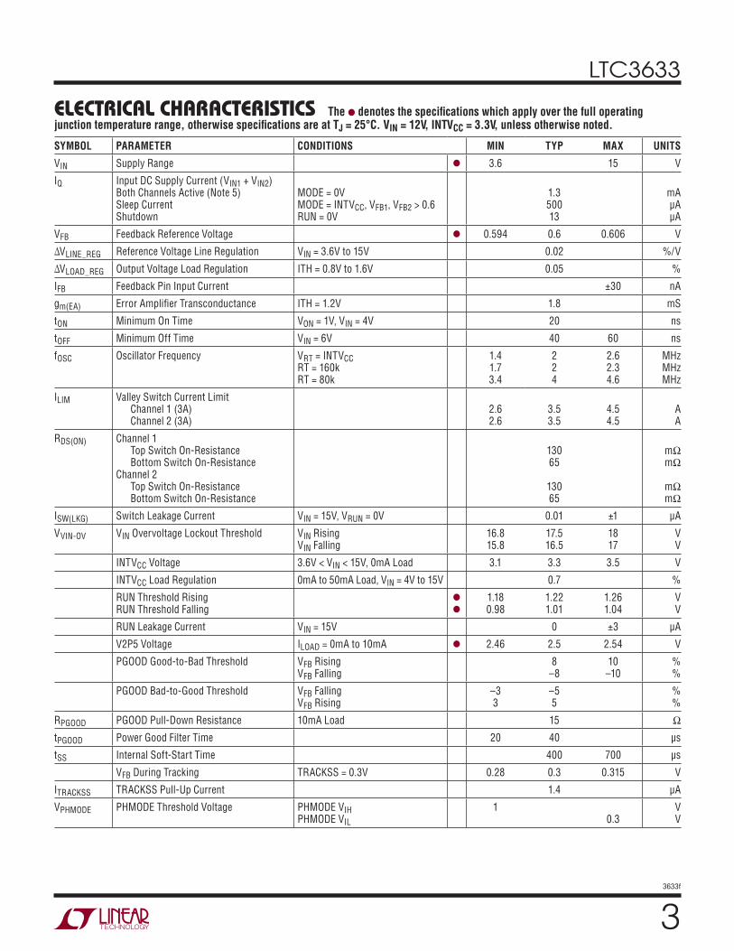
ELECTRICAL CHARACTERISTICS
SYMBOL PARAMETER CONDITIONS MIN TYP MAX UNITS
VIN Supply Range l 3.6 15 V
IQ Input DC Supply Current (VIN1 + VIN2)Both Channels Active (Note 5)Sleep CurrentShutdown
MODE = 0VMODE = INTVCC, VFB1, VFB2 > 0.6RUN = 0V
1.350013
mAμAμA
VFB Feedback Reference Voltage l 0.594 0.6 0.606 V
ΔVLINE_REG Reference Voltage Line Regulation VIN = 3.6V to 15V 0.02 %/V
ΔVLOAD_REG Output Voltage Load Regulation ITH = 0.8V to 1.6V 0.05 %
IFB Feedback Pin Input Current ±30 nA
gm(EA) Error Amplifi er Transconductance ITH = 1.2V 1.8 mS
tON Minimum On Time VON = 1V, VIN = 4V 20 ns
tOFF Minimum Off Time VIN = 6V 40 60 ns
fOSC Oscillator Frequency VRT = INTVCCRT = 160kRT = 80k
1.41.73.4
224
2.62.34.6
MHzMHzMHz
ILIM Valley Switch Current Limit Channel 1 (3A) Channel 2 (3A)
2.62.6
3.53.5
4.54.5
AA
RDS(ON) Channel 1 Top Switch On-Resistance Bottom Switch On-ResistanceChannel 2 Top Switch On-Resistance Bottom Switch On-Resistance
13065
13065
mΩmΩ
mΩmΩ
ISW(LKG) Switch Leakage Current VIN = 15V, VRUN = 0V 0.01 ±1 μA
VVIN-OV VIN Overvoltage Lockout Threshold VIN RisingVIN Falling
16.815.8
17.516.5
1817
VV
INTVCC Voltage 3.6V < VIN < 15V, 0mA Load 3.1 3.3 3.5 V
INTVCC Load Regulation 0mA to 50mA Load, VIN = 4V to 15V 0.7 %
RUN Threshold RisingRUN Threshold Falling
l
l
1.180.98
1.221.01
1.261.04
VV
RUN Leakage Current VIN = 15V 0 ±3 μA
V2P5 Voltage ILOAD = 0mA to 10mA l 2.46 2.5 2.54 V
PGOOD Good-to-Bad Threshold VFB RisingVFB Falling
8–8
10–10
%%
PGOOD Bad-to-Good Threshold VFB FallingVFB Rising
–33
–55
%%
RPGOOD PGOOD Pull-Down Resistance 10mA Load 15 Ω
tPGOOD Power Good Filter Time 20 40 μs
tSS Internal Soft-Start Time 400 700 μs
VFB During Tracking TRACKSS = 0.3V 0.28 0.3 0.315 V
ITRACKSS TRACKSS Pull-Up Current 1.4 μA
VPHMODE PHMODE Threshold Voltage PHMODE VIHPHMODE VIL
10.3
VV
The l denotes the specifi cations which apply over the full operating junction temperature range, otherwise specifi cations are at TJ = 25°C. VIN = 12V, INTVCC = 3.3V, unless otherwise noted.
LTC3633
43633f
ELECTRICAL CHARACTERISTICS
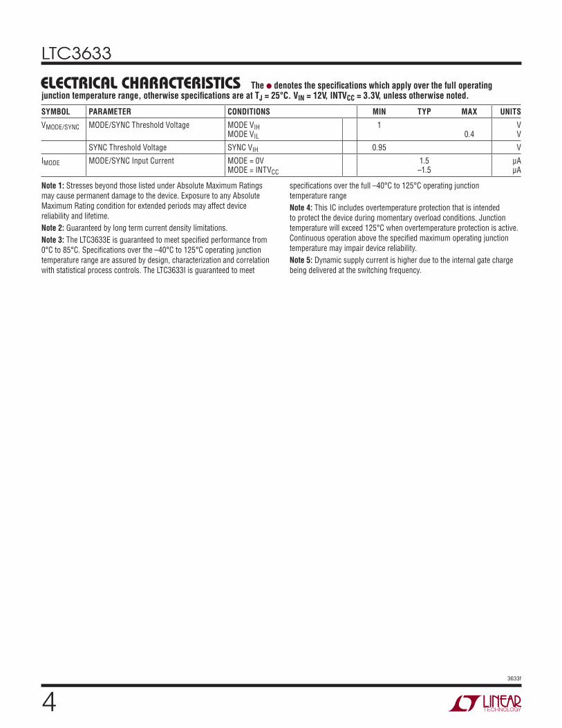
Note 1: Stresses beyond those listed under Absolute Maximum Ratings
may cause permanent damage to the device. Exposure to any Absolute
Maximum Rating condition for extended periods may affect device
reliability and lifetime.
Note 2: Guaranteed by long term current density limitations.
Note 3: The LTC3633E is guaranteed to meet specifi ed performance from
0°C to 85°C. Specifi cations over the –40°C to 125°C operating junction
temperature range are assured by design, characterization and correlation
with statistical process controls. The LTC3633I is guaranteed to meet
SYMBOL PARAMETER CONDITIONS MIN TYP MAX UNITS
VMODE/SYNC MODE/SYNC Threshold Voltage MODE VIHMODE VIL
10.4
VV
SYNC Threshold Voltage SYNC VIH 0.95 V
IMODE MODE/SYNC Input Current MODE = 0VMODE = INTVCC
1.5–1.5
μAμA
The l denotes the specifi cations which apply over the full operating junction temperature range, otherwise specifi cations are at TJ = 25°C. VIN = 12V, INTVCC = 3.3V, unless otherwise noted.
specifi cations over the full –40°C to 125°C operating junction
temperature range
Note 4: This IC includes overtemperature protection that is intended
to protect the device during momentary overload conditions. Junction
temperature will exceed 125°C when overtemperature protection is active.
Continuous operation above the specifi ed maximum operating junction
temperature may impair device reliability.
Note 5: Dynamic supply current is higher due to the internal gate charge
being delivered at the switching frequency.
LTC3633
53633f
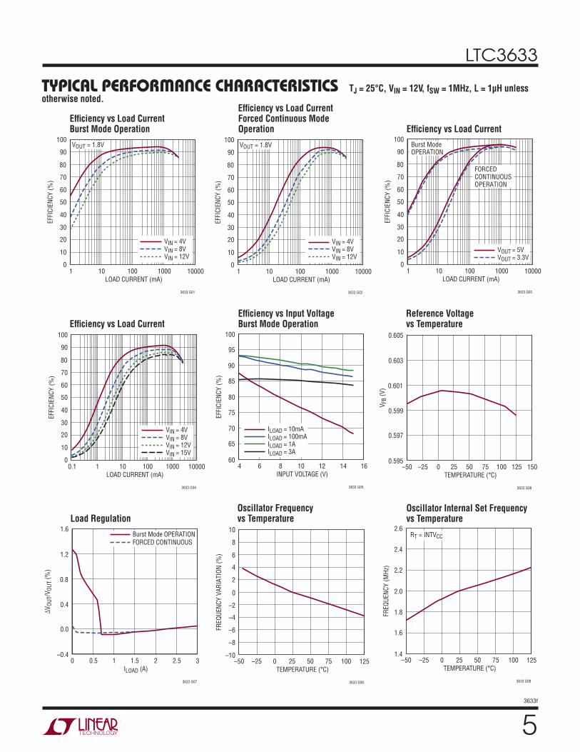
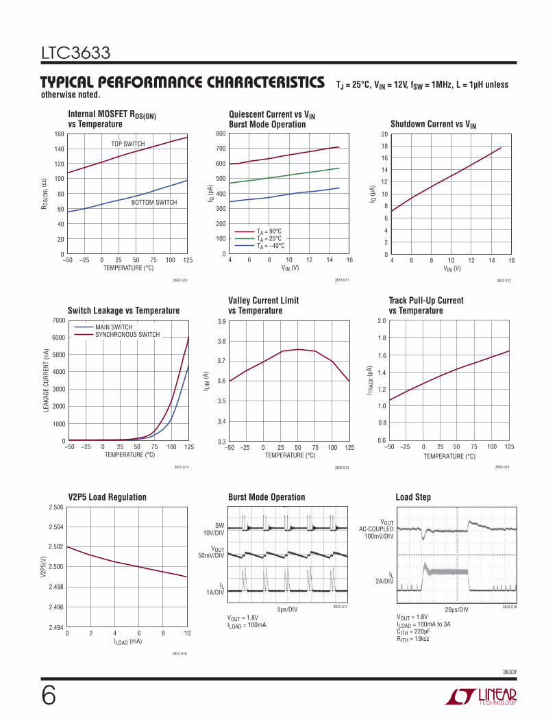
TYPICAL PERFORMANCE CHARACTERISTICS
Effi ciency vs Load CurrentEffi ciency vs Input VoltageBurst Mode Operation
Load RegulationOscillator Frequency vs Temperature
Effi ciency vs Load CurrentBurst Mode Operation
Effi ciency vs Load CurrentForced Continuous Mode Operation Effi ciency vs Load Current
TJ = 25°C, VIN = 12V, fSW = 1MHz, L = 1μH unless otherwise noted.
Oscillator Internal Set Frequency vs Temperature
Reference Voltage vs Temperature
10
EFF
ICIE
NC
Y (
%)
10
30
40
50
70
100 10000
3633 G01
20
80
100
90
60
10 1000
VIN = 4VVIN = 8VVIN = 12V
LOAD CURRENT (mA)
VOUT = 1.8V
10
EFF
ICIE
NC
Y (
%)
10
30
40
50
70
100 10000
3633 G02
20
80
100
90
60
10 1000
VIN = 4VVIN = 8VVIN = 12V
LOAD CURRENT (mA)
VOUT = 1.8V
10
EFF
ICIE
NC
Y (
%)
10
30
40
50
70
100 10000
3633 G03
20
80
100
90
60
10 1000
VOUT = 5VVOUT = 3.3V
LOAD CURRENT (mA)
Burst ModeOPERATION
FORCEDCONTINUOUSOPERATION
4
EFF
ICIE
NC
Y (
%)
65
70
75
85
8 16
3633 G05
60
90
100
95
80
6 10 12 14
ILOAD = 10mAILOAD = 100mAILOAD = 1AILOAD = 3A
INPUT VOLTAGE (V)0.1 1
0
EFF
ICIE
NC
Y (
%)
10
30
40
50
70
100 10000
3633 G04
20
80
100
90
60
10 1000
LOAD CURRENT (mA)
VIN = 4VVIN = 8VVIN = 12VVIN = 15V
–50
VFB
(V
)
0.597
0.599
50 150
3633 G06
0.595
0.601
0.605
0.603
25–25 0 75 100 125
TEMPERATURE (°C)
0
ΔV
OU
T/V
OU
T (
%)
0.0
0.4
1.5 3
3633 G07
–0.4
0.8
1.6
1.2
10.5 2 2.5
ILOAD (A)
Burst Mode OPERATION
FORCED CONTINUOUS
–50
FREQ
UEN
CY
VA
RIA
TIO
N (
%)
–8
–6
–4
–2
0
2
4
6
8
25 125
3633 G08
–10
10
0–25 50 75 100
TEMPERATURE (°C)
–50
FREQ
UEN
CY
(M
Hz)
1.6
1.8
2.0
2.2
2.4
25 125
3633 G09
1.4
2.6
0–25 50 75 100
TEMPERATURE (°C)
RT = INTVCC
LTC3633
63633f
Burst Mode Operation
Internal MOSFET RDS(ON) vs Temperature
Quiescent Current vs VIN Burst Mode Operation
Switch Leakage vs TemperatureValley Current Limit vs Temperature
Track Pull-Up Current vs Temperature
TYPICAL PERFORMANCE CHARACTERISTICS
Shutdown Current vs VIN
V2P5 Load Regulation Load Step
4
I Q (
μA
)
100
200
300
500
8 16
3633 G11
0
600
800
700
400
6 10 12 14
TA = 90°CTA = 25°CTA = –40°C
VIN (V)4
I Q (
μA
)
2
4
6
10
8 16
3633 G12
0
12
20
16
18
14
8
6 10 12 14
VIN (V)
–50
LEA
KA
GE C
UR
REN
T (
nA
)
1000
2000
3000
5000
0 125100
3633 G13
0
6000
7000
4000
–25 25 50 75
TEMPERATURE (°C)
MAIN SWITCHSYNCHRONOUS SWITCH
TJ = 25°C, VIN = 12V, fSW = 1MHz, L = 1μH unless otherwise noted.
TEMPERATURE (°C)
–50
1.4
1.6
2.0
25 75
3633 G15
1.2
1.0
–25 0 50 100 125
0.8
0.6
1.8
I TR
AC
K (
μA
)
–50
I LIM
(A
)
3.4
3.5
50
3633 G14
3.3
3.7
3.6
3.9
3.8
25–25 0 75 100 125
TEMPERATURE (°C)
0
V2P
5(V
)
2.496
2.498
6
3633 G16
2.494
2.502
2.500
2.506
2.504
42 8 10
ILOAD (mA)
IL1A/DIV
SW10V/DIV
5μs/DIV3633 G17
VOUT50mV/DIV
VOUT = 1.8VILOAD = 100mA
IL2A/DIV
20μs/DIV3633 G18
VOUTAC-COUPLED
100mV/DIV
VOUT = 1.8VILOAD = 100mA to 3ACITH = 220pFRITH = 13kΩ
–50
RD
S(O
N)
(Ω)
20
40
60
80
100
120
140
25 125
3633 G10
0
160
0–25 50 75 100
TEMPERATURE (°C)
TOP SWITCH
BOTTOM SWITCH
LTC3633
73633f
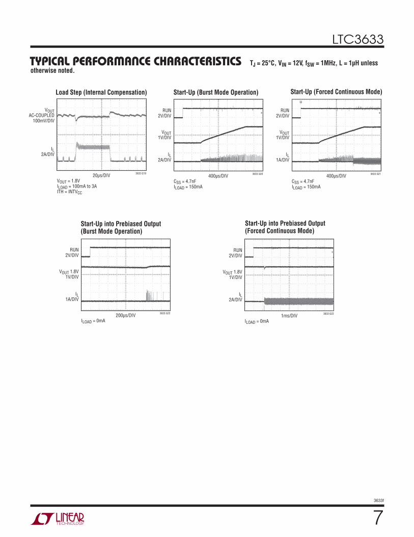
TYPICAL PERFORMANCE CHARACTERISTICS
Start-Up into Prebiased Output (Forced Continuous Mode)
Load Step (Internal Compensation)
Start-Up into Prebiased Output (Burst Mode Operation)
Start-Up (Burst Mode Operation)
TJ = 25°C, VIN = 12V, fSW = 1MHz, L = 1μH unless otherwise noted.
Start-Up (Forced Continuous Mode)
IL2A/DIV
20μs/DIV3633 G19
VOUTAC-COUPLED
100mV/DIV
VOUT = 1.8VILOAD = 100mA to 3AITH = INTVCC
IL2A/DIV
400μs/DIV3633 G20
RUN2V/DIV
VOUT1V/DIV
CSS = 4.7nFILOAD = 150mA
IL1A/DIV
400μs/DIV3633 G21
RUN2V/DIV
VOUT1V/DIV
CSS = 4.7nFILOAD = 150mA
IL1A/DIV
200μs/DIV3633 G22
RUN2V/DIV
VOUT 1.8V1V/DIV
ILOAD = 0mA
IL2A/DIV
1ms/DIV3633 G22
RUN2V/DIV
VOUT 1.8V1V/DIV
ILOAD = 0mA
LTC3633
83633f
PIN FUNCTIONSPGOOD1 (Pin 1/Pin 4): Channel 1 Open-Drain Power Good Output Pin. PGOOD1 is pulled to ground when the voltage on the VFB1 pin is not within ±8% (typical) of the internal 0.6V reference. PGOOD1 becomes high imped-ance once the VFB1 pin returns to within ±5% (typical) of the internal reference.
PHMODE (Pin 2/Pin 5): Phase Select Input. Tie this pin to ground to force both channels to switch in phase. Tie this pin to INTVCC to force both channels to switch 180° out of phase. Do not fl oat this pin.
RUN1 (Pin 3/Pin 6): Channel 1 Regulator Enable Pin. Enables channel 1 operation by tying RUN above 1.22V. Tying it below 1V places the part into shutdown. Do not fl oat this pin.
MODE/SYNC (Pin 4/Pin 7): Mode Select and External Synchronization Input. Tie this pin to ground to force continuous synchronous operation at all output loads. Floating this pin or tying it to INTVCC enables high effi ciency Burst Mode operation at light loads. Drive this pin with a clock to synchronize the LTC3633 switching. An internal phase-locked loop will force the bottom power NMOS’s turn on signal to be synchronized with the rising edge of the CLKIN signal. When this pin is driven with a clock, forced continuous mode is automatically selected.
RT (Pin 5/Pin 8): Oscillator Frequency Program Pin. Connect an external resistor (between 80k to 640k) from this pin to SGND in order to program the frequency from 500kHz to 4MHz. When RT is tied to INTVCC, the switching frequency will default to 2MHz.
RUN2 (Pin 6/Pin 9): Channel 2 Regulator Enable Pin. Enables channel 2 operation by tying RUN above 1.22V. Tying it below 1V places the part into shutdown. Do not fl oat this pin.
SGND (Pin 7/Pin 10): Signal Ground Pin. This pin should have a low noise connection to reference ground. The feedback resistor network, external compensation network, and RT resistor should be connected to this ground.
PGOOD2 (Pin 8/Pin 11): Channel 2 Open-Drain Power Good Output Pin. PGOOD2 is pulled to ground when the voltage on the VFB2 pin is not within 8% (typical) of the internal 0.6V reference. PGOOD2 becomes high imped-
ance once the VFB2 pin returns to within ±5% (typical) of the internal reference.
VFB2 (Pin 9/Pin 12): Channel 2 Output Feedback Voltage Pin. Input to the error amplifi er that compares the feedback voltage to the internal 0.6V reference voltage. Connect this pin to a resistor divider network to program the desired output voltage.
TRACKSS2 (Pin 10/Pin 13): Output Tracking and Soft-Start Input Pin for Channel 2. Forcing a voltage below 0.6V on this pin bypasses the internal reference input to the error amplifi er. The LTC3633 will servo the FB pin to the TRACK voltage under this condition. Above 0.6V, the tracking func-tion stops and the internal reference resumes control of the error amplifi er. An internal 1.4μA pull up current from INTVCC allows a soft start function to be implemented by connecting a capacitor between this pin and SGND.
ITH2 (Pin 11/Pin 14): Channel 2 Error Amplifi er Output and Switching Regulator Compensation Pin. Connect this pin to appropriate external components to compensate the regulator loop frequency response. Connect this pin to INTVCC to use the default internal compensation.
VON2 (Pin 12/Pin 15): On-Time Voltage Input for Chan-nel 2. This pin sets the voltage trip point for the on-time comparator. Tying this pin to the output voltage makes the on-time proportional to VOUT2 when VOUT2 < 6V. When VOUT2 > 6V, switching frequency may become higher than the set frequency. The pin impedance is nominally 180kΩ.
SW2 (Pins 13, 14/Pins 16, 17): Channel 2 Switch Node Connection to External Inductor. Voltage swing of SW is from a diode voltage drop below ground to VIN.
VIN2 (Pins 15, 16/Pins 18, 19): Power Supply Input for Channel 2. Input voltage to the on chip power MOSFETs on channel 2. This input is capable of operating from a different supply voltage than VIN1.
BOOST2 (Pin 17/Pin 20): Boosted Floating Driver Supply for Channel 2. The (+) terminal of the bootstrap capacitor connects to this pin while the (–) terminal connects to the SW pin. The normal operation voltage swing of this pin ranges from a diode voltage drop below INTVCC up to VIN+INTVCC.
(QFN/TSSOP)
LTC3633
93633f
PIN FUNCTIONSV2P5 (Pin 18/Pin 21): 2.5V Regulator Output. Outputs a regulated 2.5V supply voltage capable of supplying 10mA. Bypass this pin with a minimum of 1μF low ESR ceramic capacitor. Tie this pin to INTVCC when this output is not being used in the application.
INTVCC (Pin 19/Pin 22): Internal 3.3V Regulator Output. The internal power drivers and control circuits are powered from this voltage. Decouple this pin to power ground with a minimum of 1μF low ESR ceramic capacitor.
BOOST1 (Pin 20/Pin 23): Boosted Floating Driver Supply for Channel 1. The (+) terminal of the bootstrap capacitor connects to this pin while the (–) terminal connects to the SW pin. The normal operation voltage swing of this pin ranges from a diode voltage drop below INTVCC up to VIN + INTVCC.
VIN1 (Pins 21,22/Pins 24, 25): Power Supply Input for Channel 1. Input voltage to the on chip power MOSFETs on channel 1. The internal LDO for INTVCC is powered off of this pin.
SW1 (Pins 23,24/Pins 26, 27): Channel 1 Switch Node Connection to External Inductor. Voltage swing of SW is from a diode voltage drop below ground to VIN.
VON1 (Pin 25/Pin 28): On-Time Voltage Input for Chan-nel 1. This pin sets the voltage trip point for the on-time comparator. Tying this pin to the regulated output volt-age makes the on-time proportional to VOUT1 when VOUT1 < 6V. When VOUT1 > 6V, switching frequency may become higher than the set frequency. The pin impedance is nominally 180kΩ.
ITH1 (Pin 26/Pin 1): Channel 1 Error Amplifi er Output and Switching Regulator Compensation Pin. Connect this pin to appropriate external components to compensate the regulator loop frequency response. Connect this pin to INTVCC to use the default internal compensation.
TRACKSS1 (Pin 27/Pin 2): Output Tracking and Soft-Start Input Pin for Channel 1. Forcing a voltage below 0.6V on this pin bypasses the internal reference input to the error amplifi er. The LTC3633 will servo the FB pin to the TRACK voltage. Above 0.6V, the tracking function stops and the internal reference resumes control of the error amplifi er. An internal 1.4μA pull up current from INTVCC allows a soft-start function to be implemented by connecting a capacitor between this pin and SGND.
VFB1 (Pin 28/Pin 3): Channel 1 Output Feedback Voltage Pin. Input to the error amplifi er that compares the feedback voltage to the internal 0.6V reference voltage. Connect this pin to a resistor divider network to program the desired output voltage.
PGND (Exposed Pad Pin 29/Exposed Pad Pin 29): Power Ground Pin. The (–) terminal of the input bypass capaci-tor, CIN, and the (–) terminal of the output capacitor, COUT, should be tied to this pin with a low impedance connec-tion. This pin must be soldered to the PCB to provide low impedance electrical contact to power ground and good thermal contact to the PCB.
LTC3633
103633f
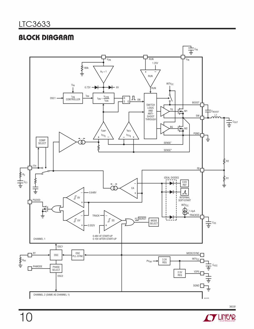
BLOCK DIAGRAM
0.72V 6V
VON VIN
CIN
1.25V
INTVCC
INTVCC
RUN
–+
+
ITH
PGOOD
AV = 1
tON =VVON
IION
ION
VIN
ICMP IREV
OSC1
180k
ON
TGM1
BOOST
SW
PGND
FB
SENSE–
SENSE+
1.4μA
0.6VREF
M2BG
SWITCHLOGICAND
ANTI-SHOOT
THROUGH
IONCONTROLLER
COMPSELECT
OSCOSC
PLL-SYNC
PHASESELECT
MODESELECT
R
S Q
CBOOST
L1
COUT
– –+
–
+EA
CC1
RC
0.648V
0.552V
TRACK
0.48V AT START-UP0.10V AFTER START-UPCHANNEL 1
CHANNEL 2 (SAME AS CHANNEL 1)
3633 BD
OSC1
OSC2
RT
RRT
PHMODE
R2
R1
INTERNALSOFT-START
IDEAL DIODES
–
–
+
+
–
+
BURSTFC
3.3VREG
PVIN1
MODE/SYNC
TRACKSS
V2P5
SGND
INTVCC
CVCC
2.5VREG
CSS
RUN
RUN
0V
UV SS
LTC3633
113633f
OPERATIONThe LTC3633 is a dual-channel, current mode monolithic step down regulator capable of providing 3A of output current from each channel. Its unique controlled on-time architecture allows extremely low step-down ratios while maintaining a constant switching frequency. Each channel is enabled by raising the voltage on the RUN pin above 1.22V nominally.
Main Control Loop
In normal operation, the internal top power MOSFET is turned on for a fi xed interval determined by a fi xed one-shot timer (“ON” signal in Block Diagram). When the top power MOSFET turns off, the bottom power MOSFET turns on until the current comparator ICMP trips, thus restarting the one shot timer and initiating the next cycle. Inductor current is measured by sensing the voltage drop across the SW and PGND nodes of the bottom power MOSFET. The voltage on the ITH pin sets the comparator threshold corresponding to inductor valley current. The error ampli-fi er EA adjusts this ITH voltage by comparing an internal 0.6V reference to the feedback signal VFB derived from the output voltage. If the load current increases, it causes a drop in the feedback voltage relative to the internal refer-ence. The ITH voltage then rises until the average inductor current matches that of the load current.
The operating frequency is determined by the value of the RT resistor, which programs the current for the internal oscillator. An internal phase-locked loop servos the switch-ing regulator on-time to track the internal oscillator edge and force a constant switching frequency. A clock signal can be applied to the MODE/SYNC pin to synchronize the switching frequency to an external source. The regulator defaults to forced continuous operation once the clock signal is applied.
At light load currents, the inductor current can drop to zero and become negative. In Burst Mode operation, a current reversal comparator (IREV) detects the negative inductor current and shuts off the bottom power MOSFET, result-ing in discontinuous operation and increased effi ciency. Both power MOSFETs will remain off until the ITH volt-age rises above the zero current level to initiate another cycle. During this time, the output capacitor supplies the load current and the part is placed into a low current sleep mode. Discontinuous mode operation is disabled
by tying the MODE/SYNC pin to ground, which forces continuous synchronous operation regardless of output load current.
“Power Good” Status Output
The PGOOD open-drain output will be pulled low if the regulator output exits a ±8% window around the regulation point. This condition is released once regulation within a ±5% window is achieved. To prevent unwanted PGOOD glitches during transients or dynamic VOUT changes, the LTC3633 PGOOD falling edge includes a fi lter time of ap-proximately 40μs.
VIN Overvoltage Protection
In order to protect the internal power MOSFET devices against transient voltage spikes, the LTC3633 constantly monitors each VIN pin for an overvoltage condition. When VIN rises above 17.5V, the regulator suspends operation by shutting off both power MOSFETs on the correspond-ing channel. Once VIN drops below 16.5V, the regulator immediately resumes normal operation. The regulator does not execute its soft-start function when exiting an overvoltage condition.
Out-Of-Phase Operation
Tying the PHMODE pin high sets the SW2 falling edge to be 180° out of phase with the SW1 falling edge. There is a signifi cant advantage to running both channels out of phase. When running the channels in phase, both top-side MOSFETs are on simultaneously, causing large current pulses to be drawn from the input capacitor and supply at the same time.
When running the LTC3633 channels out of phase, the large current pulses are interleaved, effectively reducing the amount of time the pulses overlap. Thus, the total RMS input current is decreased, which both relaxes the capacitance requirements for the VIN bypass capacitors and reduces the voltage noise on the supply line.
One potential disadvantage to this confi guration occurs when one channel is operating at 50% duty cycle. In this situation, switching noise can potentially couple from one channel to the other, resulting in frequency jitter on one or both channels. This effect can be mitigated with a well designed board layout.
LTC3633
123633f
APPLICATIONS INFORMATIONA general LTC3633 application circuit is shown on the fi rst page of this data sheet. External component selection is largely driven by the load requirement and switching frequency. Component selection typically begins with the selection of the inductor L and resistor RT. Once the inductor is chosen, the input capacitor, CIN, and the out-put capacitor, COUT, can be selected. Next, the feedback resistors are selected to set the desired output voltage. Finally, the remaining optional external components can be selected for functions such as external loop compensation, track/soft-start, VIN UVLO, and PGOOD.
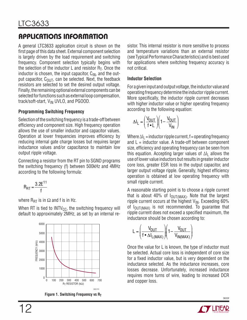
Programming Switching Frequency
Selection of the switching frequency is a trade-off between effi ciency and component size. High frequency operation allows the use of smaller inductor and capacitor values. Operation at lower frequencies improves effi ciency by reducing internal gate charge losses but requires larger inductance values and/or capacitance to maintain low output ripple voltage.
Connecting a resistor from the RT pin to SGND programs the switching frequency (f) between 500kHz and 4MHz according to the following formula:
RRT =
3.2E11
f
where RRT is in Ω and f is in Hz.
When RT is tied to INTVCC, the switching frequency will default to approximately 2MHz, as set by an internal re-
sistor. This internal resistor is more sensitive to process and temperature variations than an external resistor (see Typical Performance Characteristics) and is best used for applications where switching frequency accuracy is not critical.
Inductor Selection
For a given input and output voltage, the inductor value and operating frequency determine the inductor ripple current. More specifi cally, the inductor ripple current decreases with higher inductor value or higher operating frequency according to the following equation:
IL =VOUTf • L
1–VOUTVIN
Where ΔIL = inductor ripple current, f = operating frequency and L = inductor value. A trade-off between component size, effi ciency and operating frequency can be seen from this equation. Accepting larger values of ΔIL allows the use of lower value inductors but results in greater inductor core loss, greater ESR loss in the output capacitor, and larger output voltage ripple. Generally, highest effi ciency operation is obtained at low operating frequency with small ripple current.
A reasonable starting point is to choose a ripple current that is about 40% of IOUT(MAX). Note that the largest ripple current occurs at the highest VIN. Exceeding 60% of IOUT(MAX) is not recommended. To guarantee that ripple current does not exceed a specifi ed maximum, the inductance should be chosen according to:
L =VOUT
f • IL(MAX)1–
VOUTVIN(MAX)
Once the value for L is known, the type of inductor must be selected. Actual core loss is independent of core size for a fi xed inductor value, but is very dependent on the inductance selected. As the inductance increases, core losses decrease. Unfortunately, increased inductance requires more turns of wire, leading to increased DCR and copper loss.0
FREQ
UEN
CY
(kH
z)
1000
2000
3000
5000
200 700600
3633 F01
0
6000
4000
100 300 400 500
RT RESISTOR (kΩ)
Figure 1. Switching Frequency vs RT
LTC3633
133633f
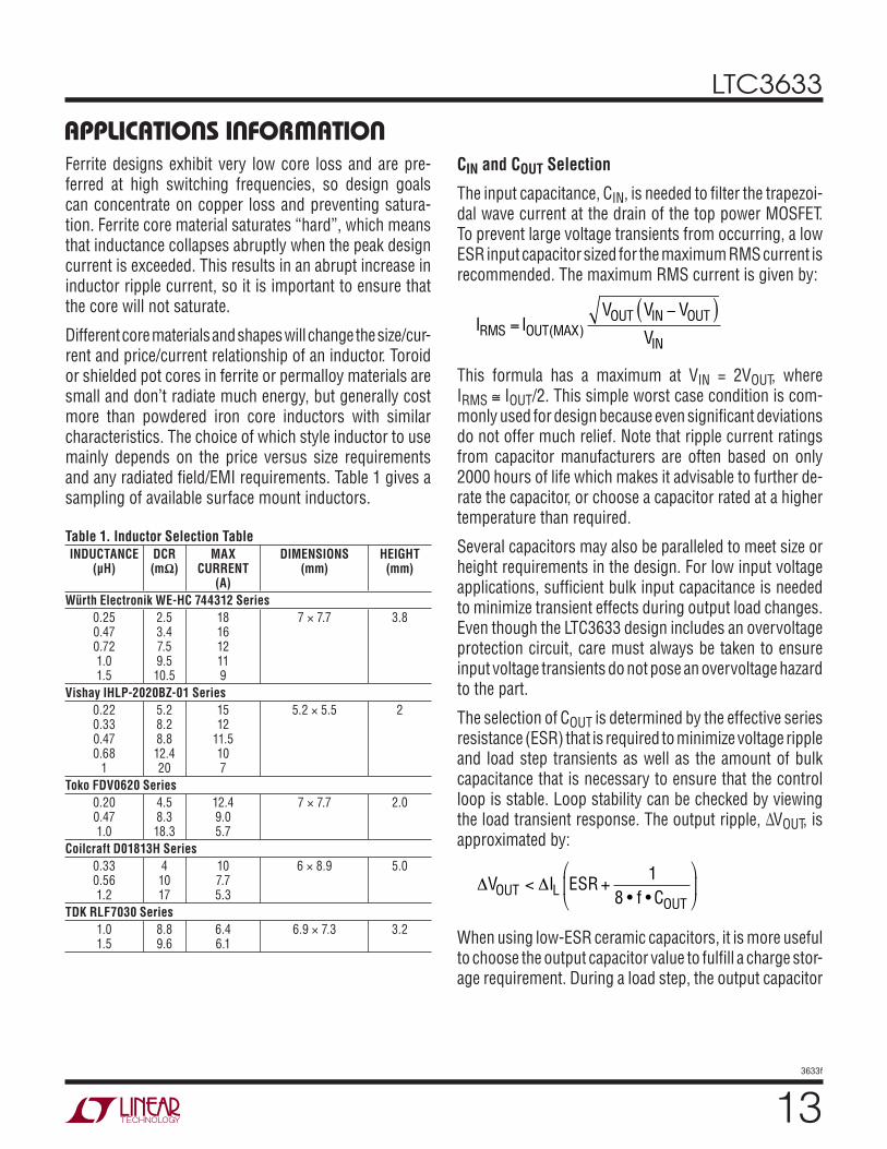
APPLICATIONS INFORMATIONFerrite designs exhibit very low core loss and are pre-ferred at high switching frequencies, so design goals can concentrate on copper loss and preventing satura-tion. Ferrite core material saturates “hard”, which means that inductance collapses abruptly when the peak design current is exceeded. This results in an abrupt increase in inductor ripple current, so it is important to ensure that the core will not saturate.
Different core materials and shapes will change the size/cur-rent and price/current relationship of an inductor. Toroid or shielded pot cores in ferrite or permalloy materials are small and don’t radiate much energy, but generally cost more than powdered iron core inductors with similar characteristics. The choice of which style inductor to use mainly depends on the price versus size requirements and any radiated fi eld/EMI requirements. Table 1 gives a sampling of available surface mount inductors.
Table 1. Inductor Selection TableINDUCTANCE
(μH)DCR(mΩ)
MAXCURRENT
(A)
DIMENSIONS(mm)
HEIGHT(mm)
Würth Electronik WE-HC 744312 Series
0.250.470.721.01.5
2.53.47.59.510.5
181612119
7 × 7.7 3.8
Vishay IHLP-2020BZ-01 Series
0.220.330.470.68
1
5.28.28.812.420
1512
11.5107
5.2 × 5.5 2
Toko FDV0620 Series
0.200.471.0
4.58.318.3
12.49.05.7
7 × 7.7 2.0
Coilcraft D01813H Series
0.330.561.2
41017
107.75.3
6 × 8.9 5.0
TDK RLF7030 Series
1.01.5
8.89.6
6.46.1
6.9 × 7.3 3.2
CIN and COUT Selection
The input capacitance, CIN, is needed to fi lter the trapezoi-dal wave current at the drain of the top power MOSFET. To prevent large voltage transients from occurring, a low ESR input capacitor sized for the maximum RMS current is recommended. The maximum RMS current is given by:
I IV V V
VRMS OUT MAXOUT IN OUT
IN=
−( )( )
This formula has a maximum at VIN = 2VOUT, where IRMS ≅ IOUT/2. This simple worst case condition is com-monly used for design because even signifi cant deviations do not offer much relief. Note that ripple current ratings from capacitor manufacturers are often based on only 2000 hours of life which makes it advisable to further de-rate the capacitor, or choose a capacitor rated at a higher temperature than required.
Several capacitors may also be paralleled to meet size or height requirements in the design. For low input voltage applications, suffi cient bulk input capacitance is needed to minimize transient effects during output load changes. Even though the LTC3633 design includes an overvoltage protection circuit, care must always be taken to ensure input voltage transients do not pose an overvoltage hazard to the part.
The selection of COUT is determined by the effective series resistance (ESR) that is required to minimize voltage ripple and load step transients as well as the amount of bulk capacitance that is necessary to ensure that the control loop is stable. Loop stability can be checked by viewing the load transient response. The output ripple, ΔVOUT, is approximated by:
VOUT < IL ESR+ 18 • f • COUT
When using low-ESR ceramic capacitors, it is more useful to choose the output capacitor value to fulfi ll a charge stor-age requirement. During a load step, the output capacitor
LTC3633
143633f
APPLICATIONS INFORMATIONmust instantaneously supply the current to support the load until the feedback loop raises the switch current enough to support the load. The time required for the feedback loop to respond is dependent on the compensation and the output capacitor size. Typically, 3 to 4 cycles are required to respond to a load step, but only in the fi rst cycle does the output drop linearly. The output droop, VDROOP, is usually about 3 times the linear drop of the fi rst cycle. Thus, a good place to start is with the output capacitor size of approximately:
COUT ≈3 •ΔIOUTf • VDROOP
Though this equation provides a good approximation, more capacitance may be required depending on the duty cycle and load step requirements. The actual VDROOP should be verifi ed by applying a load step to the output.
Using Ceramic Input and Output Capacitors
Higher values, lower cost ceramic capacitors are available in small case sizes. Their high ripple current, high voltage rating and low ESR make them ideal for switching regulator applications. However, due to the self-resonant and high-Q characteristics of some types of ceramic capacitors, care must be taken when these capacitors are used at the input. When a ceramic capacitor is used at the input and the power is supplied by a wall adapter through long wires, a load step at the output can induce ringing at the VIN input. At best, this ringing can couple to the output and be mistaken as loop instability. At worst, a sudden inrush of current through the long wires can potentially cause a voltage spike at VIN large enough to damage the part. For a more detailed discussion, refer to Application Note 88.
When choosing the input and output ceramic capacitors, choose the X5R and X7R dielectric formulations. These dielectrics have the best temperature and voltage charac-teristics of all the ceramics for a given value and size.
INTVCC Regulator Bypass Capacitor
An internal low dropout (LDO) regulator produces the 3.3V supply that powers the internal bias circuitry and drives the gate of the internal MOSFET switches. The INTVCC pin connects to the output of this regulator and must have a minimum of 1μF ceramic decoupling capaci-tance to ground. The decoupling capacitor should have low impedance electrical connections to the INTVCC and PGND pins to provide the transient currents required by the LTC3633. This supply is intended only to supply ad-ditional DC load currents as desired and not intended to regulate large transient or AC behavior, as this may impact LTC3633 operation.
Boost Capacitor
The LTC3633 uses a “bootstrap” circuit to create a voltage rail above the applied input voltage VIN. Specifi cally, a boost capacitor, CBOOST, is charged to a voltage approximately equal to INTVCC each time the bottom power MOSFET is turned on. The charge on this capacitor is then used to supply the required transient current during the remainder of the switching cycle. When the top MOSFET is turned on, the BOOST pin voltage will be equal to approximately VIN + 3.3V. For most applications, a 0.1μF ceramic capacitor closely connected between the BOOST and SW pins will provide adequate performance.
Low Power 2.5V Linear Regulator
The V2P5 pin can be used as a low power 2.5V regulated rail. This pin is the output of a 10mA linear regulator powered from the INTVCC pin. Note that the power from V2P5 eventually comes from VIN1 since the INTVCC power is supplied from VIN1. When using this output, this pin must be bypassed with a 1μF ceramic capacitor. If this output is not being used, it is recommended to short this output to INTVCC to disable the regulator.
LTC3633
153633f
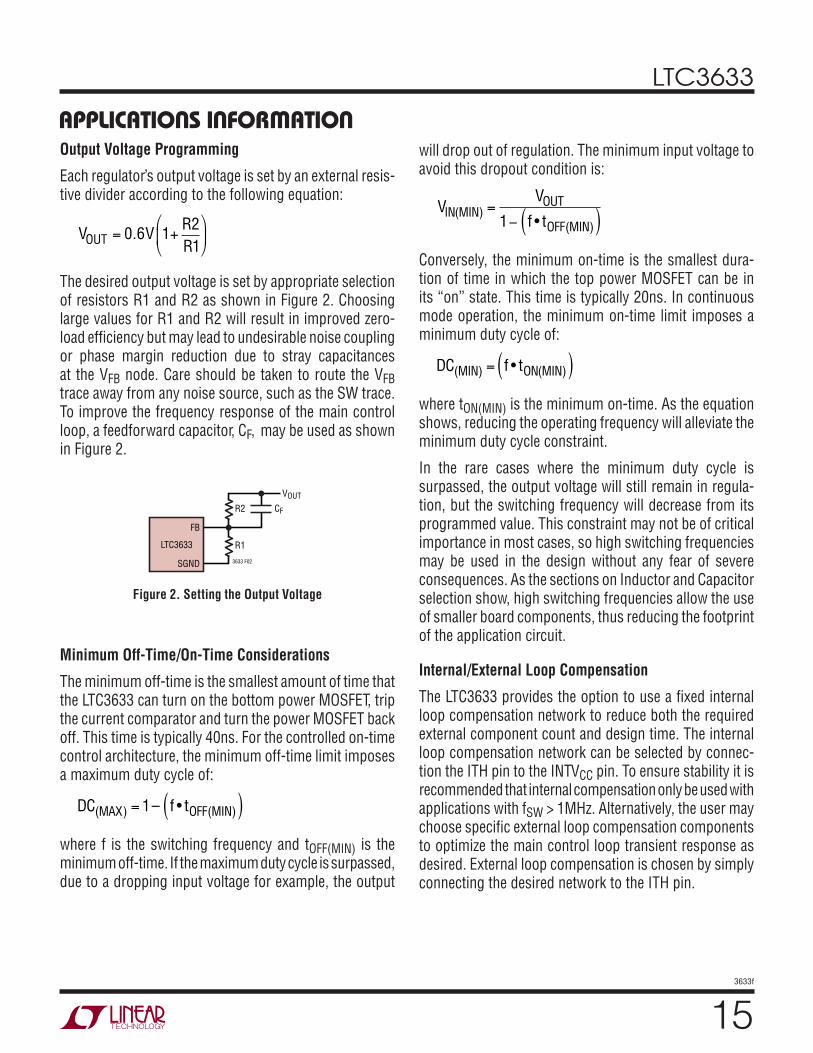
Figure 2. Setting the Output Voltage
FB
R2
R1
CF
3633 F02
VOUT
SGND
LTC3633
APPLICATIONS INFORMATIONOutput Voltage Programming
Each regulator’s output voltage is set by an external resis-tive divider according to the following equation:
VOUT = 0.6V 1+ R2R1
The desired output voltage is set by appropriate selection of resistors R1 and R2 as shown in Figure 2. Choosing large values for R1 and R2 will result in improved zero-load effi ciency but may lead to undesirable noise coupling or phase margin reduction due to stray capacitances at the VFB node. Care should be taken to route the VFB trace away from any noise source, such as the SW trace. To improve the frequency response of the main control loop, a feedforward capacitor, CF, may be used as shown in Figure 2.
Minimum Off-Time/On-Time Considerations
The minimum off-time is the smallest amount of time that the LTC3633 can turn on the bottom power MOSFET, trip the current comparator and turn the power MOSFET back off. This time is typically 40ns. For the controlled on-time control architecture, the minimum off-time limit imposes a maximum duty cycle of:
DC f tMAX OFF MIN( ) ( )– •= ( )1
where f is the switching frequency and tOFF(MIN) is the minimum off-time. If the maximum duty cycle is surpassed, due to a dropping input voltage for example, the output
will drop out of regulation. The minimum input voltage to avoid this dropout condition is:
VV
f tIN MIN
OUT
OFF MIN( )
( )•=
− ( )1
Conversely, the minimum on-time is the smallest dura-tion of time in which the top power MOSFET can be in its “on” state. This time is typically 20ns. In continuous mode operation, the minimum on-time limit imposes a minimum duty cycle of:
DC f tMIN ON MIN( ) ( )•= ( )
where tON(MIN) is the minimum on-time. As the equation shows, reducing the operating frequency will alleviate the minimum duty cycle constraint.
In the rare cases where the minimum duty cycle is surpassed, the output voltage will still remain in regula-tion, but the switching frequency will decrease from its programmed value. This constraint may not be of critical importance in most cases, so high switching frequencies may be used in the design without any fear of severe consequences. As the sections on Inductor and Capacitor selection show, high switching frequencies allow the use of smaller board components, thus reducing the footprint of the application circuit.
Internal/External Loop Compensation
The LTC3633 provides the option to use a fi xed internal loop compensation network to reduce both the required external component count and design time. The internal loop compensation network can be selected by connec-tion the ITH pin to the INTVCC pin. To ensure stability it is recommended that internal compensation only be used with applications with fSW > 1MHz. Alternatively, the user may choose specifi c external loop compensation components to optimize the main control loop transient response as desired. External loop compensation is chosen by simply connecting the desired network to the ITH pin.
LTC3633
163633f
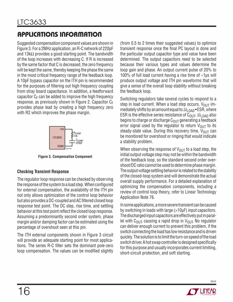
APPLICATIONS INFORMATIONSuggested compensation component values are shown in Figure 3. For a 2MHz application, an R-C network of 220pF and 13kΩ provides a good starting point. The bandwidth of the loop increases with decreasing C. If R is increased by the same factor that C is decreased, the zero frequency will be kept the same, thereby keeping the phase the same in the most critical frequency range of the feedback loop. A 10pF bypass capacitor on the ITH pin is recommended for the purposes of fi ltering out high frequency coupling from stray board capacitance. In addition, a feedforward capacitor CF can be added to improve the high frequency response, as previously shown in Figure 2. Capacitor CF provides phase lead by creating a high frequency zero with R2 which improves the phase margin.
(from 0.5 to 2 times their suggested values) to optimize transient response once the fi nal PC layout is done and the particular output capacitor type and value have been determined. The output capacitors need to be selected because their various types and values determine the loop gain and phase. An output current pulse of 20% to 100% of full load current having a rise time of ~1μs will produce output voltage and ITH pin waveforms that will give a sense of the overall loop stability without breaking the feedback loop.
Switching regulators take several cycles to respond to a step in load current. When a load step occurs, VOUT im-mediately shifts by an amount equal to ΔILOAD • ESR, where ESR is the effective series resistance of COUT. ΔILOAD also begins to charge or discharge COUT generating a feedback error signal used by the regulator to return VOUT to its steady-state value. During this recovery time, VOUT can be monitored for overshoot or ringing that would indicate a stability problem.
When observing the response of VOUT to a load step, the initial output voltage step may not be within the bandwidth of the feedback loop, so the standard second order over-shoot/DC ratio cannot be used to determine phase margin. The output voltage settling behavior is related to the stability of the closed-loop system and will demonstrate the actual overall supply performance. For a detailed explanation of optimizing the compensation components, including a review of control loop theory, refer to Linear Technology Application Note 76.
In some applications, a more severe transient can be caused by switching in loads with large (>10μF) input capacitors. The discharged input capacitors are effectively put in paral-lel with COUT, causing a rapid drop in VOUT. No regulator can deliver enough current to prevent this problem, if the switch connecting the load has low resistance and is driven quickly. The solution is to limit the turn-on speed of the load switch driver. A hot swap controller is designed specifi cally for this purpose and usually incorporates current limiting, short-circuit protection, and soft starting.
Figure 3. Compensation Component
ITH
RCOMP13k
CCOMP220pF
3633 F03
SGND
LTC3633
Checking Transient Response
The regulator loop response can be checked by observing the response of the system to a load step. When confi gured for external compensation, the availability of the ITH pin not only allows optimization of the control loop behavior but also provides a DC-coupled and AC fi ltered closed loop response test point. The DC step, rise time, and settling behavior at this test point refl ect the closed loop response. Assuming a predominantly second order system, phase margin and/or damping factor can be estimated using the percentage of overshoot seen at this pin.
The ITH external components shown in Figure 3 circuit will provide an adequate starting point for most applica-tions. The series R-C fi lter sets the dominant pole-zero loop compensation. The values can be modifi ed slightly
LTC3633
173633f
MODE/SYNC Operation
The MODE/SYNC pin is a multipurpose pin allowing both mode selection and operating frequency synchronization. Floating this pin or connecting it to INTVCC enables Burst Mode operation for superior effi ciency at low load currents at the expense of slightly higher output voltage ripple. When the MODE/SYNC pin is tied to ground, forced continuous mode operation is selected, creating the lowest fi xed output ripple at the expense of light load effi ciency.
The LTC3633 will detect the presence of the external clock signal on the MODE/SYNC pin and synchronize the internal oscillator to the phase and frequency of the incoming clock. The presence of an external clock will place both regulators into forced continuous mode operation.
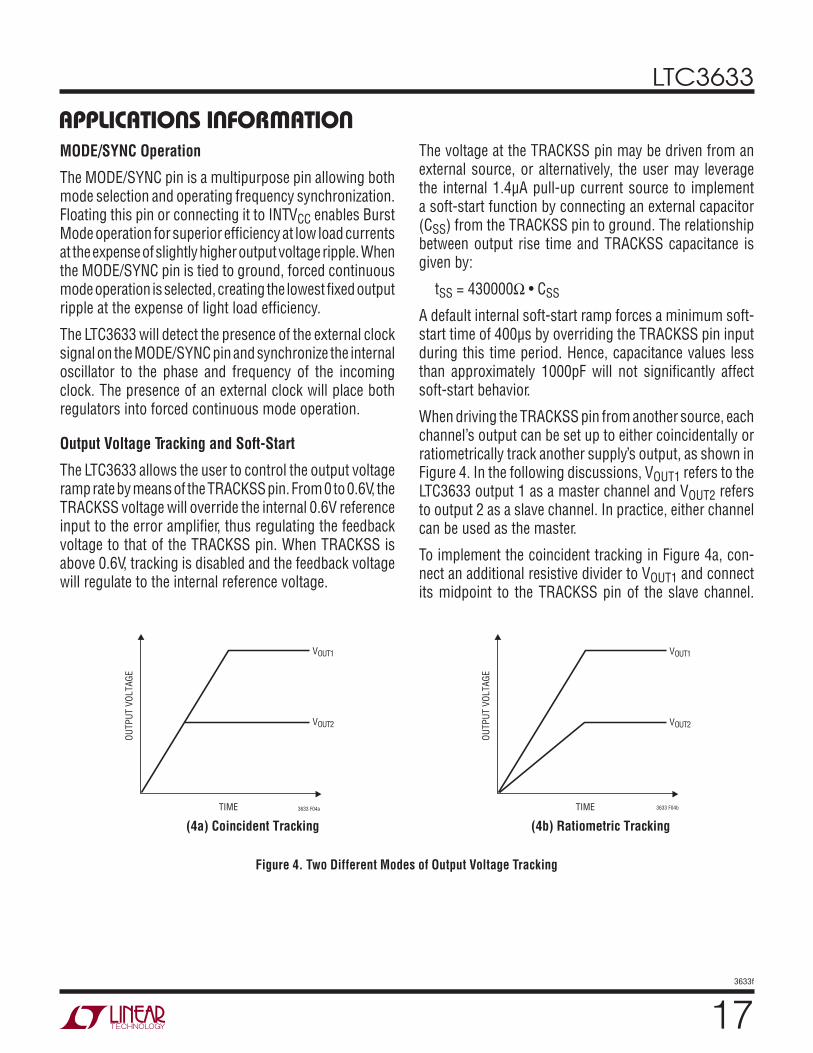
Output Voltage Tracking and Soft-Start
The LTC3633 allows the user to control the output voltage ramp rate by means of the TRACKSS pin. From 0 to 0.6V, the TRACKSS voltage will override the internal 0.6V reference input to the error amplifi er, thus regulating the feedback voltage to that of the TRACKSS pin. When TRACKSS is above 0.6V, tracking is disabled and the feedback voltage will regulate to the internal reference voltage.
APPLICATIONS INFORMATIONThe voltage at the TRACKSS pin may be driven from an external source, or alternatively, the user may leverage the internal 1.4μA pull-up current source to implement a soft-start function by connecting an external capacitor (CSS) from the TRACKSS pin to ground. The relationship between output rise time and TRACKSS capacitance is given by:
tSS = 430000Ω • CSS
A default internal soft-start ramp forces a minimum soft-start time of 400μs by overriding the TRACKSS pin input during this time period. Hence, capacitance values less than approximately 1000pF will not signifi cantly affect soft-start behavior.
When driving the TRACKSS pin from another source, each channel’s output can be set up to either coincidentally or ratiometrically track another supply’s output, as shown in Figure 4. In the following discussions, VOUT1 refers to the LTC3633 output 1 as a master channel and VOUT2 refers to output 2 as a slave channel. In practice, either channel can be used as the master.
To implement the coincident tracking in Figure 4a, con-nect an additional resistive divider to VOUT1 and connect its midpoint to the TRACKSS pin of the slave channel.
TIME
(4a) Coincident Tracking
VOUT1
VOUT2
OU
TP
UT V
OLTA
GE
3633 F04a
VOUT1
VOUT2
TIME 3633 F04b
(4b) Ratiometric Tracking
OU
TP
UT V
OLTA
GE
Figure 4. Two Different Modes of Output Voltage Tracking
LTC3633
183633f
APPLICATIONS INFORMATIONThe ratio of this divider should be the same as that of the slave channel’s feedback divider shown in Figure 5a. In this tracking mode, VOUT1 must be set higher than VOUT2. To implement the ratiometric tracking, the feedback pin of the master channel should connect to the TRACKSS pin of the slave channel (as in Figure 5b). By selecting different resistors, the LTC3633 can achieve different modes of tracking including the two in Figure 4.
Upon start-up, the regulator defaults to Burst Mode opera-tion until the output exceeds 80% of its fi nal value (VFB > 0.48V). Once the output reaches this voltage, the operating mode of the regulator switches to the mode selected by the MODE/SYNC pin as described above. During normal operation, if the output drops below 10% of its fi nal value (as it may when tracking down, for instance), the regula-tor will automatically switch to Burst Mode operation to prevent inductor saturation and improve TRACKSS pin accuracy.
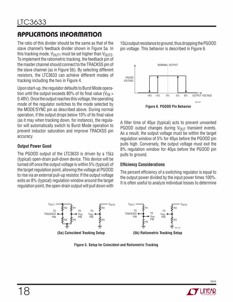
Output Power Good
The PGOOD output of the LTC3633 is driven by a 15Ω (typical) open-drain pull-down device. This device will be turned off once the output voltage is within 5% (typical) of the target regulation point, allowing the voltage at PGOOD to rise via an external pull-up resistor. If the output voltage exits an 8% (typical) regulation window around the target regulation point, the open-drain output will pull down with
15Ω output resistance to ground, thus dropping the PGOOD pin voltage. This behavior is described in Figure 6.
Figure 6. PGOOD Pin Behavior
PGOODVOLTAGE
OUTPUT VOLTAGE
NOMINAL OUTPUT
0% 8%–5% 5%
3633 F06
–8%
R3 R1
R4 R2
R3
VOUT2
R4
(5a) Coincident Tracking Setup
TOVFB1PIN
TOTRACKSS2
PIN
TOVFB2PIN
VOUT1
R1
R2
R3
VOUT2
R4
3633 F05
(5b) Ratiometric Tracking Setup
TOVFB1PIN
TOTRACKSS2
PIN
TOVFB2PIN
VOUT1
Figure 5. Setup for Coincident and Ratiometric Tracking
A fi lter time of 40μs (typical) acts to prevent unwanted PGOOD output changes during VOUT transient events. As a result, the output voltage must be within the target regulation window of 5% for 40μs before the PGOOD pin pulls high. Conversely, the output voltage must exit the 8% regulation window for 40μs before the PGOOD pin pulls to ground.
Effi ciency Considerations
The percent effi ciency of a switching regulator is equal to the output power divided by the input power times 100%. It is often useful to analyze individual losses to determine
LTC3633
193633f
APPLICATIONS INFORMATIONwhat is limiting the effi ciency and which change would produce the most improvement. Percent effi ciency can be expressed as:
% Effi ciency = 100% – (L1 + L2 + L3 +…)
where L1, L2, etc. are the individual losses as a percent-age of input power.
Although all dissipative elements in the circuit produce losses, three main sources usually account for most of the losses in LTC3633 circuits: 1) I2R losses, 2) switching losses and quiescent power loss 3) transition losses and other losses.
1. I2R losses are calculated from the DC resistances of the internal switches, RSW, and external inductor, RL. In continuous mode, the average output current fl ows through inductor L but is “chopped” between the internal top and bottom power MOSFETs. Thus, the series resistance looking into the SW pin is a function of both top and bottom MOSFET RDS(ON) and the duty cycle (DC) as follows:
RSW = (RDS(ON)TOP)(DC) + (RDS(ON)BOT)(1 – DC)
The RDS(ON) for both the top and bottom MOSFETs can be obtained from the Typical Performance Characteristics curves. Thus to obtain I2R losses:
I2R losses = IOUT2(RSW + RL)
2. The internal LDO supplies the power to the INTVCC rail. The total power loss here is the sum of the switching losses and quiescent current losses from the control circuitry.
Each time a power MOSFET gate is switched from low to high to low again, a packet of charge dQ moves from VIN to ground. The resulting dQ/dt is a current out of INTVCC that is typically much larger than the DC control bias current. In continuous mode, IGATECHG = f(QT + QB), where QT and QB are the gate charges of the internal top and bottom power MOSFETs and f is the switching frequency. For estimation purposes, (QT + QB) on each LTC3633 regulator channel is approximately 2.3nC.
To calculate the total power loss from the LDO load, simply add the gate charge current and quiescent cur-rent and multiply by VIN:
PLDO = (IGATECHG + IQ) • VIN
3. Other “hidden” losses such as transition loss, cop-per trace resistances, and internal load currents can account for additional effi ciency degradations in the overall power system. Transition loss arises from the brief amount of time the top power MOSFET spends in the saturated region during switch node transitions. The LTC3633 internal power devices switch quickly enough that these losses are not signifi cant compared to other sources.
Other losses, including diode conduction losses during dead-time and inductor core losses, generally account for less than 2% total additional loss.
Thermal Considerations
The LTC3633 requires the exposed package backplane metal (PGND) to be well soldered to the PC board to provide good thermal contact. This gives the QFN and TSSOP packages exceptional thermal properties, which are necessary to prevent excessive self-heating of the part in normal operation.
In a majority of applications, the LTC3633 does not dis-sipate much heat due to its high effi ciency and low thermal resistance of its exposed-back QFN package. However, in applications where the LTC3633 is running at high ambi-ent temperature, high VIN, high switching frequency, and maximum output current load, the heat dissipated may exceed the maximum junction temperature of the part. If the junction temperature reaches approximately 150°C, both power switches will be turned off until temperature returns to 140°C.
To prevent the LTC3633 from exceeding the maximum junction temperature of 125°C, the user will need to do some thermal analysis. The goal of the thermal analysis

LTC3633
203633f
APPLICATIONS INFORMATIONis to determine whether the power dissipated exceeds the maximum junction temperature of the part. The tempera-ture rise is given by:
TRISE = PD • θJA
As an example, consider the case when one of the regula-tors is used in an application where VIN = 12V, IOUT = 2A, frequency = 2MHz, VOUT = 1.8V. From the RDS(ON) graphs in the Typical Performance Characteristics section, the top switch on-resistance is nominally 140mΩ and the bottom switch on-resistance is nominally 80mΩ at 70°C ambient. The equivalent power MOSFET resistance RSW is:
RDS(ON)TOP • 1.8V
12V+RDS(ON)BOT • 10.2V
12V=89mΩ
From the previous section’s discussion on gate drive, we estimate the total gate drive current through the LDO to be 2MHz • 2.3nC = 4.6mA, and IQ of one channel is 0.65mA (see Electrical Characteristics). Therefore, the total power dissipated by a single regulator is:
PD = IOUT2 • RSW + VIN • (IGATECHG + IQ)
PD = (2A)2 • (0.089Ω) + (12V) • (4.6mA + 0.65mA) = 0.419W
Running two regulators under the same conditions would result in a power dissipation of 0.838W. The QFN 5mm × 4mm package junction-to-ambient thermal resistance, θJA, is around 43°C/W. Therefore, the junction temperature of the regulator operating in a 70°C ambient temperature is approximately:
TJ = 0.838W • 43°C/W + 70°C = 106°C
which is below the maximum junction temperature of 125°C. With higher ambient temperatures, a heat sink or cooling fan should be considered to drop the junc-tion-to-ambient thermal resistance. Alternatively, the TSSOP package may be a better choice for high power applications, since it has better thermal properties than the QFN package.
Remembering that the above junction temperature is obtained from an RDS(ON) at 70°C, we might recalculate the junction temperature based on a higher RDS(ON) since it increases with temperature. Redoing the calculation assuming that RSW increased 12% at 106°C yields a new
junction temperature of 109°C. If the application calls for a higher ambient temperature and/or higher load currents, care should be taken to reduce the temperature rise of the part by using a heat sink or air fl ow.
Figure 7 is a temperature derating curve based on the DC1347 demo board (QFN package). It can be used to estimate the maximum allowable ambient temperature for given DC load currents in order to avoid exceeding the maximum operating junction temperature of 125°C.
Figure 7. Temperature Derating Curve for DC1347 Demo Circuit
Junction Temperature Measurement
The junction-to-ambient thermal resistance will vary de-pending on the size and amount of heat sinking copper on the PCB board where the part is mounted, as well as the amount of air fl ow on the device. In order to properly evaluate this thermal resistance, the junction temperature needs to be measured. A clever way to measure the junction temperature directly is to use the internal junction diode on one of the pins (PGOOD) to measure its diode voltage change based on ambient temperature change.
First remove any external passive component on the PGOOD pin, then pull out 100μA from the PGOOD pin to turn on its internal junction diode and bias the PGOOD pin to a negative voltage. With no output current load, measure the PGOOD voltage at an ambient temperature of 25°C, 75°C and 125°C to establish a slope relationship between the delta voltage on PGOOD and delta ambient temperature. Once this slope is established, then the junction temperature rise can be measured as a function
0
CH
AN
NEL 1
LO
AD
CU
RR
EN
T (
A)
0.5
1.0
1.5
2.0
3.0
2.5
50 125
3633 F07
0
3.5
25 75 100
MAXIMUM ALLOWABLE AMBIENT
TEMPERATURE (°C)
CH2 LOAD = 0ACH2 LOAD = 1ACH2 LOAD = 2ACH2 LOAD = 3A
LTC3633
213633f
of power loss in the package with corresponding output load current. Although making this measurement with this method does violate absolute maximum voltage ratings on the PGOOD pin, the applied power is so low that there should be no signifi cant risk of damaging the device.
Board Layout Considerations
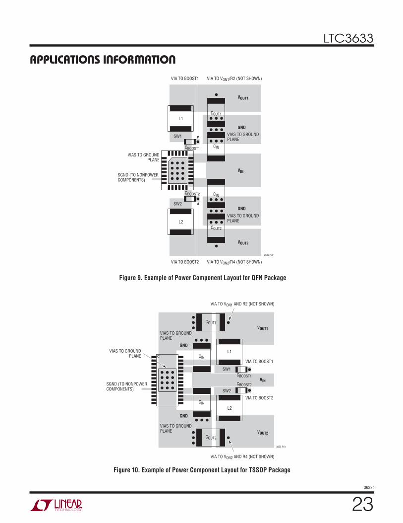
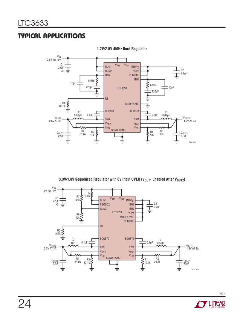
When laying out the printed circuit board, the following checklist should be used to ensure proper operation of the LTC3633. Check the following in your layout:
1) Do the input capacitors connect to the VIN and PGND pins as close as possible? These capacitors provide the AC current to the internal power MOSFETs and their drivers.
2) The output capacitor, COUT, and inductor L should be closely connected to minimize loss. The (–) plate of COUT should be closely connected to both PGND and the (–) plate of CIN.
3) The resistive divider, (e.g. R1 to R4 in Figure 8) must be connected between the (+) plate of COUT and a ground line terminated near SGND. The feedback signal VFB should be routed away from noisy components and traces, such as the SW line, and its trace length should be minimized. In addition, the RT resistor and loop compensation components should be terminated to SGND.
4) Keep sensitive components away from the SW pin. The RT resistor, the compensation components, the feedback resistors, and the INTVCC bypass capacitor should all be routed away from the SW trace and the inductor L.
5) A ground plane is preferred, but if not available, the signal and power grounds should be segregated with both connecting to a common, low noise reference point. The connection to the PGND pin should be made with a minimal resistance trace from the reference point.
APPLICATIONS INFORMATION6) Flood all unused areas on all layers with copper in order
to reduce the temperature rise of power components. These copper areas should be connected to the exposed backside of the package (PGND).
Refer to Figures 9 and 10 for board layout examples.
Design Example
As a design example, consider using the LTC3633 in an application with the following specifi cations: VIN(MAX)
= 13.2V, VOUT1 = 1.8V, VOUT2 = 3.3V, IOUT(MAX) = 3A, IOUT(MIN) = 10mA, f = 2MHz, VDROOP ~ (5% • VOUT). The following discussion will use equations from the previous sections.
Because effi ciency is important at both high and low load current, Burst Mode operation will be utilized.
First, the correct RT resistor value for 2MHz switching fre-quency must be chosen. Based on the equation discussed earlier, RT should be 160k; the closest standard value is 162k. RT can be tied to INTVCC if switching frequency accuracy is not critical.
Next, determine the channel 1 inductor value for about 40% ripple current at maximum VIN:
L1= 1.8V2MHz • 1.2A
1 1.8V13.2V
=0.64μH
A standard value of 0.68μH should work well here. Solv-ing the same equation for channel 2 results in a 1μH inductor.
COUT will be selected based on the charge storage require-ment. For a VDROOP of 90mV for a 3A load step:
COUT1≈3 •ΔIOUTf0VDROOP
=3 •(3A)
(2MHz)(90mV)=50μF
LTC3633
223633f
APPLICATIONS INFORMATIONA 47μF ceramic capacitor should be suffi cient for channel 1. Solving the same equation for channel 2 (using 5% of VOUT for VDROOP) results in 27μF of capacitance (22μF is the closest standard value).
CIN should be sized for a maximum current rating of:
I A
V V V
VARMS =
−( )=3
1 8 13 2 1 8
13 21
. . .
.
Solving this equation for channel 2 results in an RMS input current of 1.3A. Decoupling each VIN input with a 47μF ceramic capacitor should be adequate for most applications.
Lastly, the feedback resistors must be chosen. Picking R1 and R3 to be 12.1k, R2 and R4 are calculated to be:
R2 = (12.1k) • 1.8V0.6V
– 1 = 24.2k
R4 = (12.1k) • 3.3V0.6V
– 1 = 54.5k
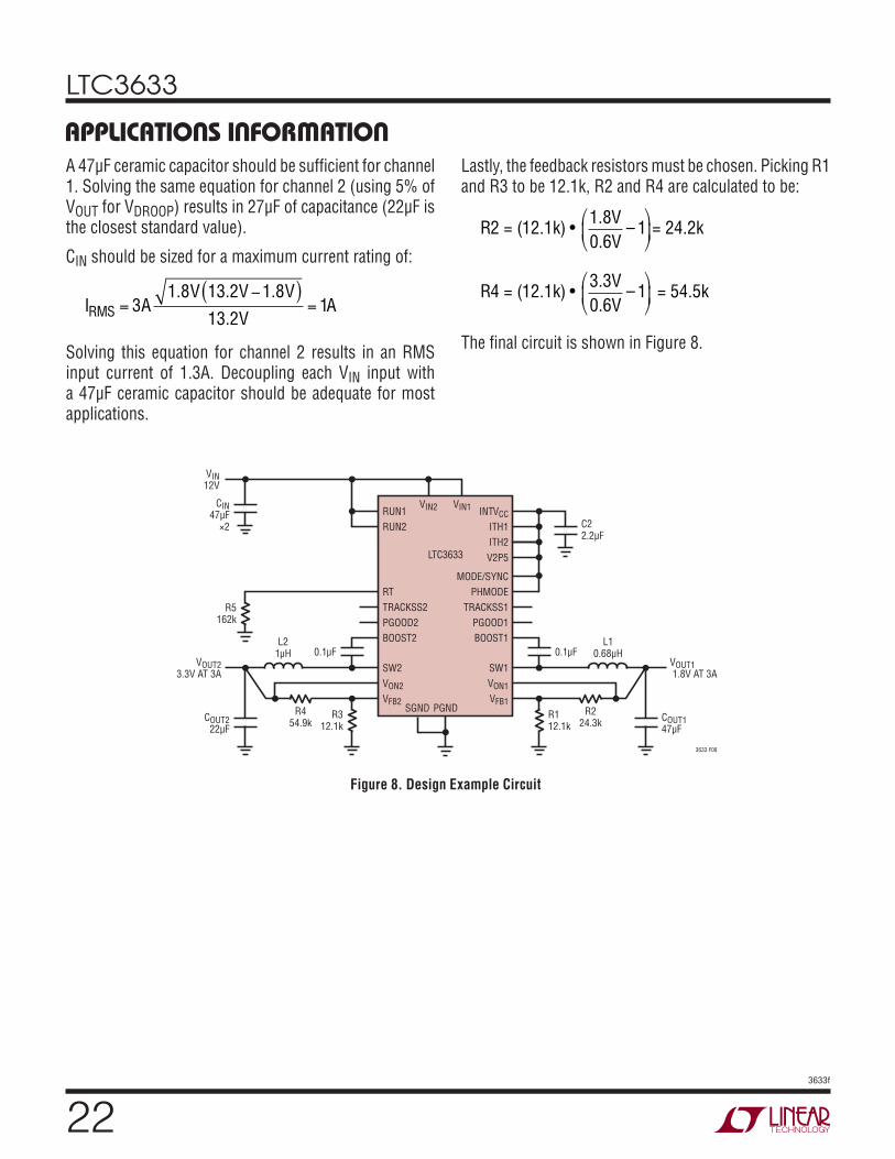
The fi nal circuit is shown in Figure 8.
RUN1
RUN2
RT
TRACKSS2
PGOOD2
LTC3633
BOOST2
3633 F08
0.1μFL2
1μH
R454.9k
R312.1k
SW2
VON2
VIN2 VIN1
VFB2
PHMODE
TRACKSS1
PGOOD1
BOOST1
SW1
VON1
VFB1
COUT222μF
VOUT2 3.3V AT 3A
0.1μFL1
0.68μH
R224.3k
R112.1k
COUT147μF
VOUT1 1.8V AT 3A
VIN 12V
CIN47μF
×2
R5162k
MODE/SYNC
ITH1
ITH2
V2P5
INTVCCC22.2μF
PGNDSGND
Figure 8. Design Example Circuit
LTC3633
233633f
Figure 9. Example of Power Component Layout for QFN Package
APPLICATIONS INFORMATION
Figure 10. Example of Power Component Layout for TSSOP Package
SW2
CBOOST2
CBOOST1
SW1
VIAS TO GROUNDPLANE
VIAS TO GROUNDPLANE
VIAS TO GROUNDPLANE
VIA TO BOOST1
VIA TO BOOST2 VIA TO VON2/R4 (NOT SHOWN)
VIA TO VON1/R2 (NOT SHOWN)
VOUT2
GND
VIN
GND
VOUT1
SGND (TO NONPOWERCOMPONENTS)
3633 F09
COUT2
CIN
CIN
COUT1
L2
L1
SW1
SW2
VIAS TO GROUNDPLANE
VIAS TO GROUNDPLANE
VIAS TO GROUNDPLANE
VIA TO BOOST2
VIA TO BOOST1
VIA TO VON2 AND R4 (NOT SHOWN)
VIA TO VON1 AND R2 (NOT SHOWN)
VOUT2
VOUT1
SGND (TO NONPOWERCOMPONENTS)
3633 F10
L1
L2
COUT2
COUT1
CIN
CIN
GND
GND
VIN
CBOOST1
CBOOST2
LTC3633
243633f
TYPICAL APPLICATIONS
1.2V/2.5V 4MHz Buck Regulator
RUN1
RUN2
RT
LTC3633
BOOST2
3633 TA02
0.1μFL2
0.82μH
R431.6k
R310k
SW2
VON2
VIN2 VIN1
VFB2
BOOST1
MODE/SYNC
SW1
VON1
VFB1
COUT222μF
VOUT2 2.5V AT 3A
0.1μFL1
0.47μH
R210k
R110k
COUT147μF
VOUT1 1.2V AT 3A
VIN 3.6V TO 15V
C122μF
×2
220pF
10pF
R580.6k
ITH2
V2P5
PHMODE
6.98k ITH1
INTVCCC22.2μF
220pF
6.98k10pF
PGNDSGND
3.3V/1.8V Sequenced Regulator with 6V Input UVLO (VOUT1 Enabled After VOUT2)
RUN1
PGOOD2
RUN2
RT
LTC3633
BOOST2
3633 TA05
0.1μFL2
1μH
R454.9k
R312.1k
SW2
VON2
VIN2 VIN1
VFB2
BOOST1
SW1
VON1
VFB1
COUT222μF
VOUT2 3.3V AT 3A
0.1μFL1
0.68μH
R224.3k
R112.1k
COUT147μF
VOUT1 1.8V AT 3A
VIN 6V TO 15V
C147μF
×2
R5162k
R7154k
R840k
V2P5
ITH1
ITH2
INTVCCC22.2μF
MODE/SYNC
PHMODE
R6100k
PGNDSGND
LTC3633
253633f
TYPICAL APPLICATIONS
1.2V/1.8V Buck Regulator with Coincident Tracking and 6V Input UVLO
RUN1
RUN2
RT
LTC3633
BOOST2
3633 TA03
0.1μFL2
0.47μH
R410k
R310k
SW2
VON2
VIN2 VIN1
VFB2
BOOST1
SW1
VON1
VFB1
COUT268μF
VOUT2 1.2V AT 3A
0.1μFL1
0.68μH
R64.99k
R110k
COUT147μF
VOUT1 1.8V AT 3A
VIN 3.6V TO 15V
C147μF
×2
R5162k
R7154k
R840k
TRACKSS2
R215k
MODE/SYNC
ITH1
ITH2
INTVCCC22.2μF
V2P5
PHMODE
PGNDSGND
LTC3633
263633f
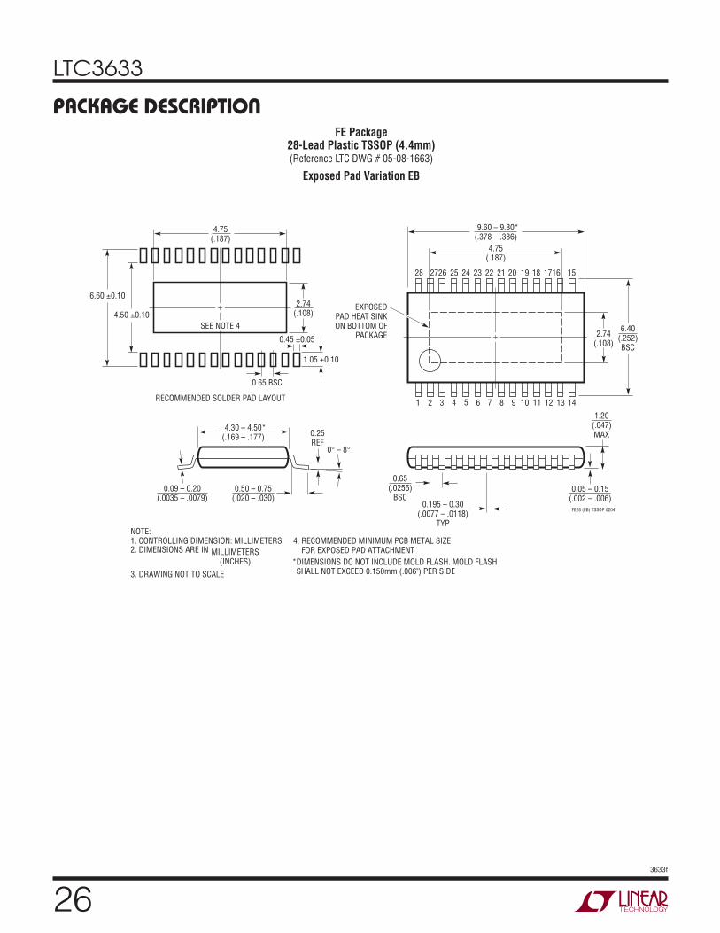
PACKAGE DESCRIPTIONFE Package
28-Lead Plastic TSSOP (4.4mm)(Reference LTC DWG # 05-08-1663)
Exposed Pad Variation EB
FE28 (EB) TSSOP 0204
0.09 – 0.20(.0035 – .0079)
0° – 8°
0.25REF
0.50 – 0.75(.020 – .030)
4.30 – 4.50*(.169 – .177)
1 3 4 5 6 7 8 9 10 11 12 13 14
192022 21 151618 17
9.60 – 9.80*(.378 – .386)
4.75(.187)
2.74(.108)
28 2726 25 24 23
1.20(.047)MAX
0.05 – 0.15(.002 – .006)
0.65(.0256)
BSC0.195 – 0.30
(.0077 – .0118)TYP
2RECOMMENDED SOLDER PAD LAYOUT
EXPOSEDPAD HEAT SINKON BOTTOM OF
PACKAGE0.45 ±0.05
0.65 BSC
4.50 ±0.10
6.60 ±0.10
1.05 ±0.10
4.75(.187)
2.74(.108)
MILLIMETERS(INCHES) *DIMENSIONS DO NOT INCLUDE MOLD FLASH. MOLD FLASH
SHALL NOT EXCEED 0.150mm (.006") PER SIDE
NOTE:1. CONTROLLING DIMENSION: MILLIMETERS2. DIMENSIONS ARE IN
3. DRAWING NOT TO SCALE
SEE NOTE 4
4. RECOMMENDED MINIMUM PCB METAL SIZE FOR EXPOSED PAD ATTACHMENT
6.40(.252)BSC
LTC3633
273633f
Information furnished by Linear Technology Corporation is believed to be accurate and reliable. However, no responsibility is assumed for its use. Linear Technology Corporation makes no representa-tion that the interconnection of its circuits as described herein will not infringe on existing patent rights.
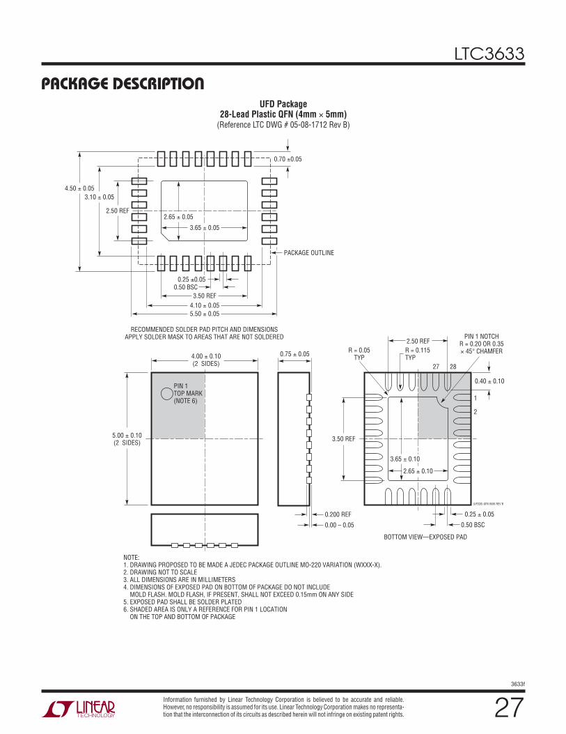
PACKAGE DESCRIPTION
4.00 ± 0.10(2 SIDES)
2.50 REF
5.00 ± 0.10(2 SIDES)
NOTE:1. DRAWING PROPOSED TO BE MADE A JEDEC PACKAGE OUTLINE MO-220 VARIATION (WXXX-X).2. DRAWING NOT TO SCALE3. ALL DIMENSIONS ARE IN MILLIMETERS4. DIMENSIONS OF EXPOSED PAD ON BOTTOM OF PACKAGE DO NOT INCLUDE MOLD FLASH. MOLD FLASH, IF PRESENT, SHALL NOT EXCEED 0.15mm ON ANY SIDE5. EXPOSED PAD SHALL BE SOLDER PLATED6. SHADED AREA IS ONLY A REFERENCE FOR PIN 1 LOCATION ON THE TOP AND BOTTOM OF PACKAGE
PIN 1TOP MARK(NOTE 6)
0.40 ± 0.10
27 28
1
2
BOTTOM VIEW—EXPOSED PAD
3.50 REF
0.75 ± 0.05 R = 0.115TYP
R = 0.05TYP
PIN 1 NOTCHR = 0.20 OR 0.35× 45° CHAMFER
0.25 ± 0.05
0.50 BSC
0.200 REF
0.00 – 0.05
(UFD28) QFN 0506 REV B
RECOMMENDED SOLDER PAD PITCH AND DIMENSIONSAPPLY SOLDER MASK TO AREAS THAT ARE NOT SOLDERED
0.70 ±0.05
0.25 ±0.050.50 BSC
2.50 REF
3.50 REF4.10 ± 0.055.50 ± 0.05
2.65 ± 0.05
3.10 ± 0.054.50 ± 0.05
PACKAGE OUTLINE
2.65 ± 0.10
3.65 ± 0.10
3.65 ± 0.05
UFD Package28-Lead Plastic QFN (4mm × 5mm)
(Reference LTC DWG # 05-08-1712 Rev B)
LTC3633
283633f
Linear Technology Corporation1630 McCarthy Blvd., Milpitas, CA 95035-7417 (408) 432-1900 ● FAX: (408) 434-0507 ● www.linear.com © LINEAR TECHNOLOGY CORPORATION 2010
LT 0110 • PRINTED IN USA
RELATED PARTS
TYPICAL APPLICATION
PART NUMBER
DESCRIPTION COMMENTS
LTC3605 15V, 5A (IOUT), 4MHz, Synchronous Step-Down DC/DC Converter
95% Effi ciency, VIN: 4V to 15V, VOUT(MIN) = 0.6V, IQ = 2mA, ISD < 15μA, 4mm × 4mm QFN-24
LTC3603 15V, 2.5A (IOUT), 3MHz, Synchronous Step-Down DC/DC Converter
95% Effi ciency, VIN: 4.5V to 15V, VOUT(MIN) = 0.6V, IQ = 75μA, ISD < 1μA, 4mm × 4mm QFN-20, MSOP-16E
LTC3602 10V, 2.5A (IOUT), 3MHz, Synchronous Step-Down DC/DC Converter
95% Effi ciency, VIN: 4.5V to 10V, VOUT(MIN) = 0.6V, IQ = 75μA, ISD < 1μA, 3mm × 3mm QFN-16, MSOP-16E
LTC3601 15V, 1.5A (IOUT), 4MHz, Synchronous Step-Down DC/DC Converter
95% Effi ciency, VIN: 4.5V to 15V, VOUT(MIN) = 0.6V, IQ = 300μA, ISD < 1μA, 4mm × 4mm QFN-20, MSOP-16E
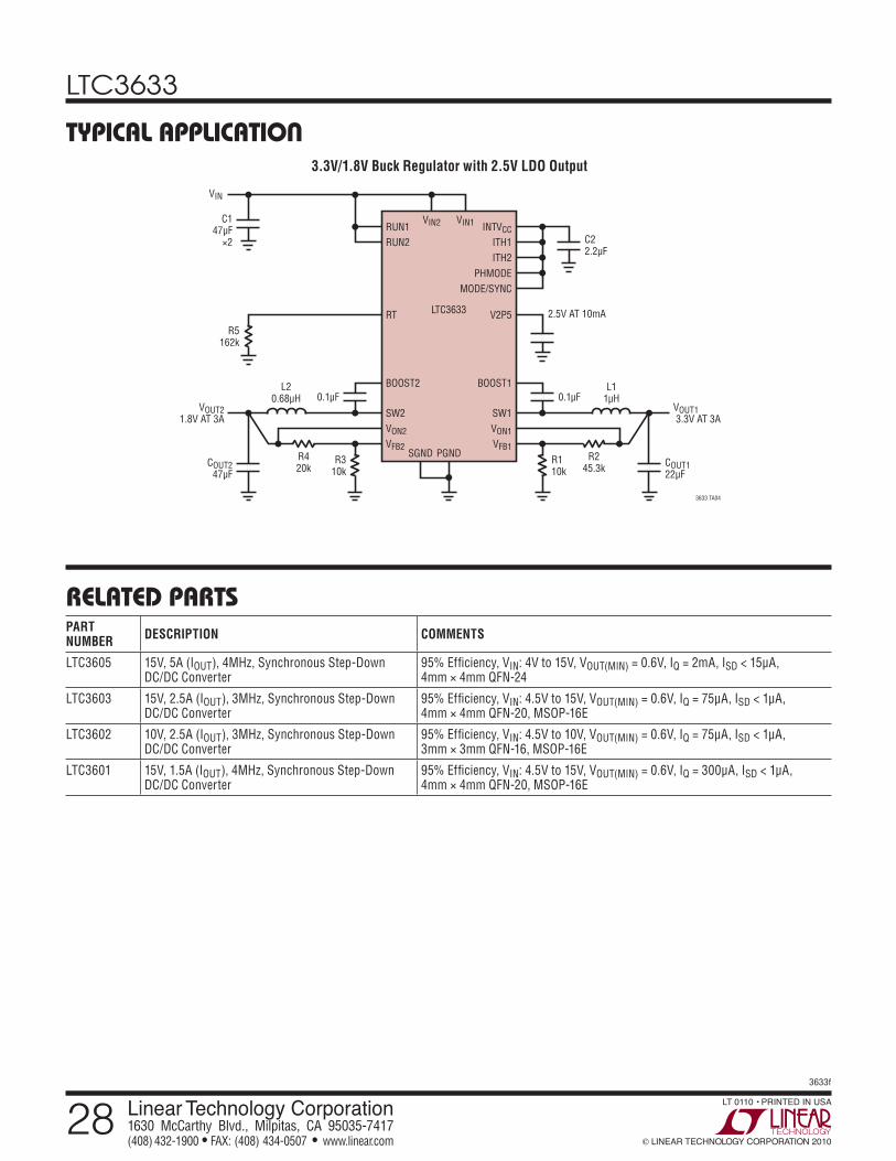
3.3V/1.8V Buck Regulator with 2.5V LDO Output
RUN1
RUN2
RTLTC3633
BOOST2
3633 TA04
0.1μFL2
0.68μH
R420k
R310k
SW2
VON2
VIN2 VIN1
VFB2
BOOST1
SW1
VON1
VFB1
COUT247μF
VOUT2 1.8V AT 3A
0.1μFL1
1μH
R245.3k
R110k
COUT122μF
VOUT1 3.3V AT 3A
2.5V AT 10mA
VIN
C147μF
×2
R5162k
V2P5
ITH1
PHMODE
ITH2
MODE/SYNC
INTVCCC22.2μF
PGNDSGND