MAX6351MAX6360 Dual/Triple-Voltage μP Supervisory Circuits · 2014-07-24 · ICC1 + ICC2 VCC1 =...
11
General Description The MAX6351–MAX6360 microprocessor (μP) supervi- sors with multiple reset voltages significantly improve system reliability and accuracy compared to separate ICs or discrete components. If any input supply voltage drops below its associated preset threshold, all reset outputs are asserted. In addition, the outputs are valid as long as either input supply voltage remains greater than +1.0V. All devices in this series have an active-low debounced manual-reset input. In addition, the MAX6358/MAX6359/ MAX6360 offer a watchdog timer input with a 46.4s startup timeout period and a 2.9s timeout period. The MAX6355/ MAX6356/MAX6357 offer an additional voltage-monitor input to monitor a third voltage. The MAX6351 features two active-low, push-pull reset outputs, one is referenced to V CC 1 and the other is refer- enced to V CC 2. The MAX6353/MAX6356/MAX6359 offer an active-low, push-pull reset output referenced to VCC1. The MAX6354/MAX6357/MAX6360 offer an active-low, push-pull reset output referenced to V CC 2. All these devices are offered with a wide variety of voltage threshold levels, as shown in the Voltage-Threshold Levels table. They are available in 5- and 6-pin SOT23 packages and oper- ate over the extended (-40°C to +85°C) temperature range. Features ● Precision Monitoring of Multiple +1.8V, +2.5V, +3.0V, +3.3V, and +5V Power-Supply Voltages ● Precision Factory-Set Power-Supply Reset Thresholds ● 20μA Supply Current ● 100ms min Power-On-Reset Pulse Width ● Debounced TTL/CMOS-Compatible Manual-Reset Input ● Watchdog Timer • 46.4s Startup Timeout • 2.9s Normal Timeout ● Fully Guaranteed Over Temperature ● Guaranteed RESET Valid to V CC 1 = 1V or V CC 2 = 1V ● Power-Supply Transient Immunity ● No External Components for Dual-Voltage Systems ● Small 5- and 6-Pin SOT23 Packages ● Low Cost Applications Note: Standard versions are shown in bold. Sample stock is generally held on the standard versions only. Contact factory for availability. *The _ _ are placeholders for the threshold voltage levels of the devices. Substitute the part number suffix in the Voltage Threshold Levels table for the desired voltage level. All devices are available in tape-and-reel only. There is a 2500 piece minimum order increment for the SOT package. Devices are available in both leaded and lead(Pb)-free packag- ing. Specify lead-free by replacing “-T” with “+T” when ordering. Pin Configurations appear at end of data sheet. Selector Guide appears at end of data sheet. 19-1508; Rev 7; 5/14 ● Computers ● Controllers ● Portable/Battery- Powered Equipment ● Intelligent Instruments ● Multivoltage Systems PART NO. SUFFIX (_ _) V CC 1 NOMINAL VOLTAGE THRESHOLD (V) V CC 2 NOMINAL VOLTAGE THRESHOLD (V) LT 4.63 3.08 LS 4.63 2.93 LR 4.63 2.63 MT 4.38 3.08 MS 4.38 2.93 MR 4.38 2.63 TZ 3.08 2.32 TY 3.08 2.19 TW 3.08 1.67 TV 3.08 1.58 SZ 2.93 2.32 SY 2.93 2.19 SW 2.93 1.67 SV 2.93 1.58 UW 2.78 1.67 UV 2.78 1.58 RW 2.63 1.67 RV 2.63 1.58 PART TEMP RANGE PIN-PACKAGE MAX6351_ _UT-T -40°C to +85°C 6 SOT23 MAX6352_ _UK-T -40°C to +85°C 5 SOT23 MAX6353_ _UK-T -40°C to +85°C 5 SOT23 MAX6354_ _UK-T -40°C to +85°C 5 SOT23 MAX6355_ _UT-T -40°C to +85°C 6 SOT23 MAX6356_ _UT-T -40°C to +85°C 6 SOT23 MAX6357_ _UT-T -40°C to +85°C 6 SOT23 MAX6358_ _UT-T -40°C to +85°C 6 SOT23 MAX6359_ _UT-T -40°C to +85°C 6 SOT23 MAX6360_ _UT-T -40°C to +85°C 6 SOT23 MAX6351–MAX6360 Dual/Triple-Voltage μP Supervisory Circuits Voltage Threshold Levels Ordering Information
Transcript of MAX6351MAX6360 Dual/Triple-Voltage μP Supervisory Circuits · 2014-07-24 · ICC1 + ICC2 VCC1 =...
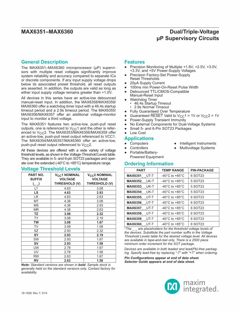
General DescriptionThe MAX6351–MAX6360 microprocessor (μP) supervi-sors with multiple reset voltages significantly improve system reliability and accuracy compared to separate ICs or discrete components. If any input supply voltage drops below its associated preset threshold, all reset outputs are asserted. In addition, the outputs are valid as long as either input supply voltage remains greater than +1.0V.All devices in this series have an active-low debounced manual-reset input. In addition, the MAX6358/MAX6359/ MAX6360 offer a watchdog timer input with a 46.4s startup timeout period and a 2.9s timeout period. The MAX6355/MAX6356/MAX6357 offer an additional voltage-monitor input to monitor a third voltage.The MAX6351 features two active-low, push-pull reset outputs, one is referenced to VCC1 and the other is refer-enced to VCC2. The MAX6353/MAX6356/MAX6359 offer an active-low, push-pull reset output referenced to VCC1. The MAX6354/MAX6357/MAX6360 offer an active-low, push-pull reset output referenced to VCC2.All these devices are offered with a wide variety of voltage threshold levels, as shown in the Voltage-Threshold Levels table. They are available in 5- and 6-pin SOT23 packages and oper-ate over the extended (-40°C to +85°C) temperature range.
Features Precision Monitoring of Multiple +1.8V, +2.5V, +3.0V,
+3.3V, and +5V Power-Supply Voltages Precision Factory-Set Power-Supply
Reset Thresholds 20μA Supply Current 100ms min Power-On-Reset Pulse Width Debounced TTL/CMOS-Compatible
Manual-Reset Input Watchdog Timer
• 46.4s Startup Timeout • 2.9s Normal Timeout
Fully Guaranteed Over Temperature Guaranteed RESET Valid to VCC1 = 1V or VCC2 = 1V Power-Supply Transient Immunity No External Components for Dual-Voltage Systems Small 5- and 6-Pin SOT23 Packages Low Cost
Applications
Note: Standard versions are shown in bold. Sample stock is generally held on the standard versions only. Contact factory for availability.
*The _ _ are placeholders for the threshold voltage levels of the devices. Substitute the part number suffix in the Voltage Threshold Levels table for the desired voltage level. All devices are available in tape-and-reel only. There is a 2500 piece minimum order increment for the SOT package.Devices are available in both leaded and lead(Pb)-free packag-ing. Specify lead-free by replacing “-T” with “+T” when ordering.Pin Configurations appear at end of data sheet. Selector Guide appears at end of data sheet.
19-1508; Rev 7; 5/14
Computers Controllers Portable/Battery-
Powered Equipment
Intelligent Instruments Multivoltage Systems
PART NO.SUFFIX
(_ _)
VCC1 NOMINALVOLTAGE
THRESHOLD (V)
VCC2 NOMINALVOLTAGE
THRESHOLD (V)LT 4.63 3.08LS 4.63 2.93LR 4.63 2.63MT 4.38 3.08MS 4.38 2.93MR 4.38 2.63TZ 3.08 2.32TY 3.08 2.19TW 3.08 1.67TV 3.08 1.58SZ 2.93 2.32SY 2.93 2.19SW 2.93 1.67SV 2.93 1.58UW 2.78 1.67UV 2.78 1.58RW 2.63 1.67RV 2.63 1.58
PART TEMP RANGE PIN-PACKAGEMAX6351_ _UT-T -40°C to +85°C 6 SOT23MAX6352_ _UK-T -40°C to +85°C 5 SOT23MAX6353_ _UK-T -40°C to +85°C 5 SOT23MAX6354_ _UK-T -40°C to +85°C 5 SOT23MAX6355_ _UT-T -40°C to +85°C 6 SOT23MAX6356_ _UT-T -40°C to +85°C 6 SOT23MAX6357_ _UT-T -40°C to +85°C 6 SOT23MAX6358_ _UT-T -40°C to +85°C 6 SOT23MAX6359_ _UT-T -40°C to +85°C 6 SOT23MAX6360_ _UT-T -40°C to +85°C 6 SOT23
MAX6351–MAX6360 Dual/Triple-Voltage μP Supervisory Circuits
Voltage Threshold LevelsOrdering Information
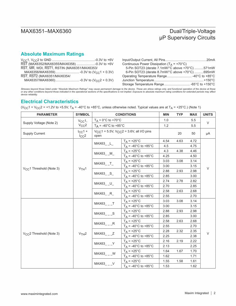
VCC1, VCC2 to GND ...............................................-0.3V to +6VRST (MAX6352/MAX6355/MAX6358) ....................-0.3V to +6VRST, MR, WDI, RST1, RSTIN (MAX6351/MAX6353/ MAX6356/MAX6359) .......................... -0.3V to (VCC1 + 0.3V)RST, RST2 (MAX6351/MAX6354/ MAX6357/MAX6360) .......................... -0.3V to (VCC2 + 0.3V)
Input/Output Current, All Pins .............................................20mAContinuous Power Dissipation (TA = +70°C) 5-Pin SOT23 (derate 7.1mW/°C above +70°C) ..........571mW 6-Pin SOT23 (derate 8.7mW/°C above +70°C) ..........695mWOperating Temperature Range ........................... -40°C to +85°CJunction Temperature ......................................................+150°CStorage Temperature Range ............................ -65°C to +150°C
(VCC1 = VCC2 = +1.2V to +5.5V, TA = -40°C to +85°C, unless otherwise noted. Typical values are at TA = +25°C.) (Note 1)
PARAMETER SYMBOL CONDITIONS MIN TYP MAX UNITS
Supply Voltage (Note 2) VCC1, VCC2
TA = 0°C to +70°C 1.0 5.5V
TA = -40°C to +85°C 1.2 5.5
Supply Current ICC1 + ICC2
VCC1 = 5.5V, VCC2 = 3.6V, all I/O pins open 20 50 µA
VCC1 Threshold (Note 3) VTH1
MAX63_ _L_TA = +25°C 4.54 4.63 4.72
V
TA = -40°C to +85°C 4.5 4.75
MAX63_ _M_TA = +25°C 4.3 4.38 4.46TA = -40°C to +85°C 4.25 4.50
MAX63_ _T_TA = +25°C 3.03 3.08 3.14TA = -40°C to +85°C 3.00 3.15
MAX63_ _S_TA = +25°C 2.88 2.93 2.98TA = -40°C to +85°C 2.85 3.00
MAX63_ _U_TA = +25°C 2.74 2.78 2.82TA = -40°C to +85°C 2.70 2.85
MAX63_ _R_TA = +25°C 2.58 2.63 2.68TA = -40°C to +85°C 2.55 2.70
VCC2 Threshold (Note 3) VTH2
MAX63_ _ _TTA = +25°C 3.03 3.08 3.14
V
TA = -40°C to +85°C 3.00 3.15
MAX63_ _ _STA = +25°C 2.88 2.93 2.98TA = -40°C to +85°C 2.85 3.00
MAX63_ _ _RTA = +25°C 2.58 2.63 2.68TA = -40°C to +85°C 2.55 2.70
MAX63_ _ _ZTA = +25°C 2.28 2.32 2.35TA = -40°C to +85°C 2.25 2.38
MAX63_ _ _YTA = +25°C 2.16 2.19 2.22TA = -40°C to +85°C 2.13 2.25
MAX63_ _ _WTA = +25°C 1.64 1.67 1.70TA = -40°C to +85°C 1.62 1.71
MAX63_ _ _VTA = +25°C 1.55 1.58 1.61TA = -40°C to +85°C 1.53 1.62
MAX6351–MAX6360 Dual/Triple-Voltage μP Supervisory Circuits
www.maximintegrated.com Maxim Integrated 2
Absolute Maximum Ratings
Stresses beyond those listed under “Absolute Maximum Ratings” may cause permanent damage to the device. These are stress ratings only, and functional operation of the device at these or any other conditions beyond those indicated in the operational sections of the specifications is not implied. Exposure to absolute maximum rating conditions for extended periods may affect device reliability.
Electrical Characteristics
(VCC1 = VCC2 = +1.2V to +5.5V, TA = -40°C to +85°C, unless otherwise noted. Typical values are at TA = +25°C.) (Note 1)
PARAMETER SYMBOL CONDITIONS MIN TYP MAX UNITS
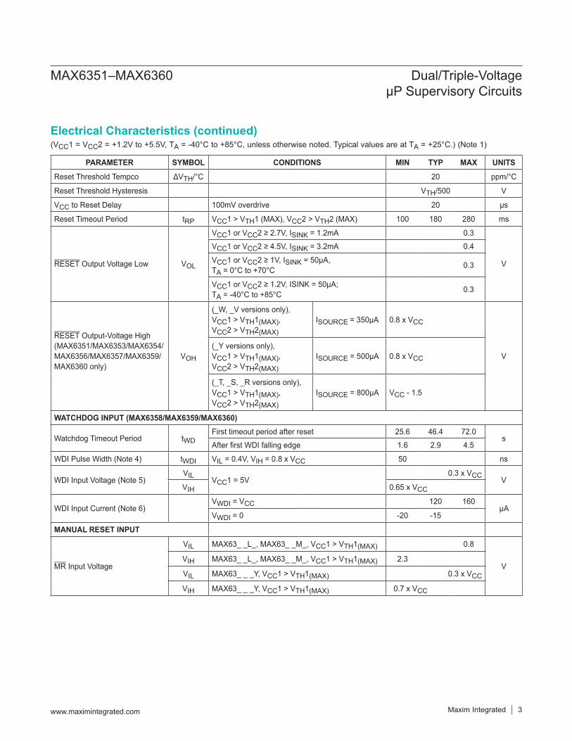
Reset Threshold Tempco ΔVTH/°C 20 ppm/°C
Reset Threshold Hysteresis VTH/500 V
VCC to Reset Delay 100mV overdrive 20 µs
Reset Timeout Period tRP VCC1 > VTH1 (MAX), VCC2 > VTH2 (MAX) 100 180 280 ms
RESET Output Voltage Low VOL
VCC1 or VCC2 ≥ 2.7V, ISINK = 1.2mA 0.3
V
VCC1 or VCC2 ≥ 4.5V, ISINK = 3.2mA 0.4
VCC1 or VCC2 ≥ 1V, ISINK = 50µA, TA = 0°C to +70°C 0.3
VCC1 or VCC2 ≥ 1.2V, ISINK = 50µA;TA = -40°C to +85°C 0.3
RESET Output-Voltage High(MAX6351/MAX6353/MAX6354/MAX6356/MAX6357/MAX6359/MAX6360 only)
VOH
(_W, _V versions only), VCC1 > VTH1(MAX), VCC2 > VTH2(MAX)
ISOURCE = 350µA 0.8 x VCC
V(_Y versions only), VCC1 > VTH1(MAX), VCC2 > VTH2(MAX)
ISOURCE = 500µA 0.8 x VCC
(_T, _S, _R versions only),VCC1 > VTH1(MAX), VCC2 > VTH2(MAX)
ISOURCE = 800µA VCC - 1.5
WATCHDOG INPUT (MAX6358/MAX6359/MAX6360)
Watchdog Timeout Period tWDFirst timeout period after reset 25.6 46.4 72.0
sAfter first WDI falling edge 1.6 2.9 4.5
WDI Pulse Width (Note 4) tWDI VIL = 0.4V, VIH = 0.8 x VCC 50 ns
WDI Input Voltage (Note 5)VIL VCC1 = 5V
0.3 x VCC VVIH 0.65 x VCC
WDI Input Current (Note 6)VWDI = VCC 120 160
µAVWDI = 0 -20 -15
MANUAL RESET INPUT
MR Input Voltage
VIL MAX63_ _L_, MAX63_ _M_, VCC1 > VTH1(MAX) 0.8
VVIH MAX63_ _L_, MAX63_ _M_, VCC1 > VTH1(MAX) 2.3
VIL MAX63_ _ _Y, VCC1 > VTH1(MAX) 0.3 x VCC
VIH MAX63_ _ _Y, VCC1 > VTH1(MAX) 0.7 x VCC
MAX6351–MAX6360 Dual/Triple-Voltage μP Supervisory Circuits
www.maximintegrated.com Maxim Integrated 3
Electrical Characteristics (continued)
(VCC1 = VCC2 = +1.2V to +5.5V, TA = -40°C to +85°C, unless otherwise noted. Typical values are at TA = +25°C.) (Note 1)
Note 1: Overtemperature limits are guaranteed by design and not production tested.Note 2: The reset output is guaranteed to be in the correct state if either VCC1 or VCC2 is within its specified region of operation.Note 3: The reset output(s) is asserted if either VCC1 or VCC2 drops below its associated trip point.Note 4: Guaranteed by design. Not production tested.Note 5: WDI is internally serviced within the watchdog timeout period if WDI is left unconnected.Note 6: The WDI input current is specified as the average input current when the WDI input is driven high or low.
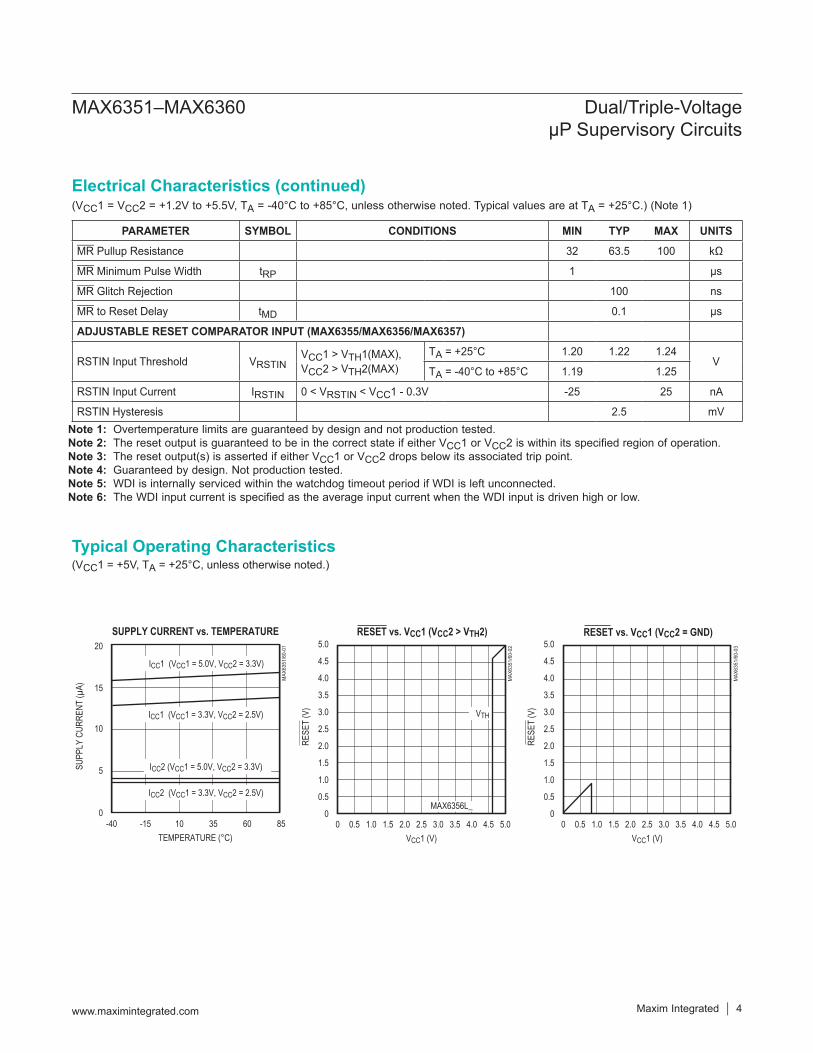
(VCC1 = +5V, TA = +25°C, unless otherwise noted.)
PARAMETER SYMBOL CONDITIONS MIN TYP MAX UNITS
MR Pullup Resistance 32 63.5 100 kΩ
MR Minimum Pulse Width tRP 1 µs
MR Glitch Rejection 100 ns
MR to Reset Delay tMD 0.1 µs
ADJUSTABLE RESET COMPARATOR INPUT (MAX6355/MAX6356/MAX6357)
RSTIN Input Threshold VRSTINVCC1 > VTH1(MAX), VCC2 > VTH2(MAX)
TA = +25°C 1.20 1.22 1.24V
TA = -40°C to +85°C 1.19 1.25
RSTIN Input Current IRSTIN 0 < VRSTIN < VCC1 - 0.3V -25 25 nA
RSTIN Hysteresis 2.5 mV
VCC1 (V)
RESET vs. VCC1 (VCC2 > VTH2)
VTH
0
1.0
0.5
2.0
1.5
3.0
2.5
3.5
4.5
4.0
5.0
0 1.0 1.5 2.00.5 2.5 3.0 3.5 4.54.0 5.0
MAX
6351
/60-
02
RESE
T (V
)
MAX6356L_0
1.0
0.5
2.0
1.5
3.0
2.5
3.5
4.5
4.0
5.0
0 1.0 1.5 2.00.5 2.5 3.0 3.5 4.54.0 5.0
MAX
6351
/60-
03
VCC1 (V)
RESE
T (V
)
RESET vs. VCC1 (VCC2 = GND)
0
5
10
15
20
-40 10-15 35 60 85
SUPPLY CURRENT vs. TEMPERATURE
MAX
6351
/60-
01
TEMPERATURE (°C)
SUPP
LY C
URRE
NT (µ
A)
ICC1 (VCC1 = 5.0V, VCC2 = 3.3V)
ICC2 (VCC1 = 5.0V, VCC2 = 3.3V)
ICC2 (VCC1 = 3.3V, VCC2 = 2.5V)
ICC1 (VCC1 = 3.3V, VCC2 = 2.5V)
MAX6351–MAX6360 Dual/Triple-Voltage μP Supervisory Circuits
www.maximintegrated.com Maxim Integrated 4
Electrical Characteristics (continued)
Typical Operating Characteristics
(VCC1 = +5V, TA = +25°C, unless otherwise noted.)
0.80
0.90
0.85
1.00
0.95
1.05
1.10
1.15
1.20
-60 -20 0-40 20 40 60 80 100
NORMALIZED RESET/WATCHDOG PERIOD vs. TEMPERATURE
MAX
6351
/60-
04
TEMPERATURE (°C)
NORM
ALIZ
ED P
ERIO
D
300
00.01 0.1 1
MAXIMUM VCC TRANSIENT DURATION vs. RESET THRESHOLD OVERDRIVE
100
50
MAX
6351
/60-
05
RESET THRESHOLD OVERDRIVE, VRST - VCC (V)
TRAN
SIEN
T DU
RATI
ON (µ
s)
150
200
250RESET OCCURS ABOVE LINE
0
50
100
150
200
250
0 0.4 0.50.2 0.30.1 0.6 0.7 0.8 0.9 1.0
RESET DELAY vs. RESET THRESHOLD OVERDRIVE
MAX
6351
/60-
06
RESET THRESHOLD OVERDRIVE, VRST - VCC (V)
RESE
T DE
LAY
(µs)
DELAY FROM FALL OF VCC1
DELAY FROM FALL OF VCC2
OPEN-DRAINOUTPUT
0
0
0
5V
3V
RST1 PUSH-PULLOUTPUT
RST2 PUSH-PULLOUTPUT
5V
PULLUP CHARACTERISTICSMAX6351/60-07
400ns/div
RPULLUP = 100kΩCLOAD = 10pF
0
5V
MANUAL-RESET INPUT TO OUTPUT DELAY
40ns/div
0
5V
MR
MAX6351/60-08
0
0
5V
5V
OPEN-DRAINOUTPUT
RST1 PUSH-PULLOUTPUT
RST2 PUSH-PULLOUTPUT
RPULLUP = 100kΩCLOAD = 10pF
MAX6351–MAX6360 Dual/Triple-Voltage μP Supervisory Circuits
Maxim Integrated 5www.maximintegrated.com
Typical Operating Characteristics (continued)
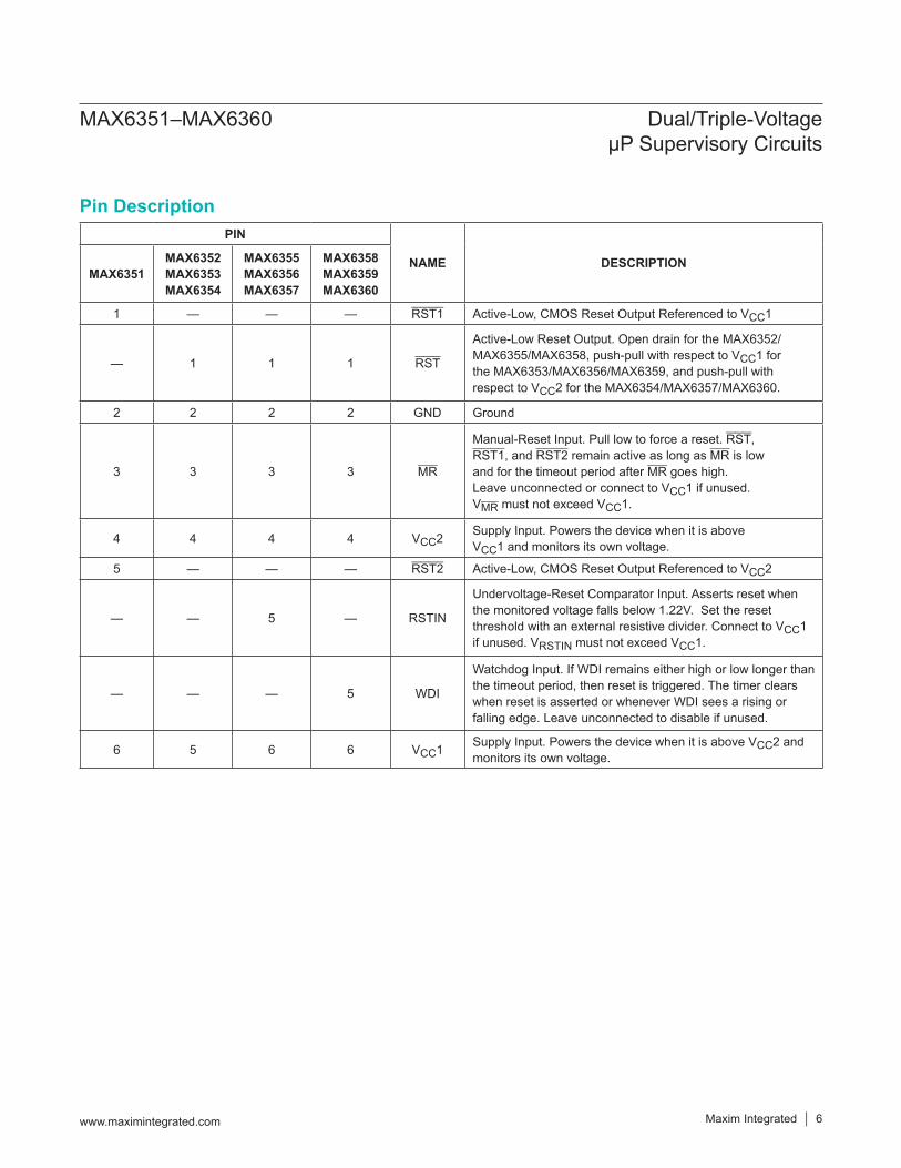
PIN
NAME DESCRIPTIONMAX6351
MAX6352MAX6353MAX6354
MAX6355MAX6356MAX6357
MAX6358MAX6359MAX6360
1 — — — RST1 Active-Low, CMOS Reset Output Referenced to VCC1
— 1 1 1 RST
Active-Low Reset Output. Open drain for the MAX6352/ MAX6355/MAX6358, push-pull with respect to VCC1 for the MAX6353/MAX6356/MAX6359, and push-pull with respect to VCC2 for the MAX6354/MAX6357/MAX6360.
2 2 2 2 GND Ground
3 3 3 3 MR
Manual-Reset Input. Pull low to force a reset. RST,RST1, and RST2 remain active as long as MR is lowand for the timeout period after MR goes high.Leave unconnected or connect to VCC1 if unused.VMR must not exceed VCC1.
4 4 4 4 VCC2 Supply Input. Powers the device when it is above VCC1 and monitors its own voltage.
5 — — — RST2 Active-Low, CMOS Reset Output Referenced to VCC2
— — 5 — RSTIN
Undervoltage-Reset Comparator Input. Asserts reset when the monitored voltage falls below 1.22V. Set the reset threshold with an external resistive divider. Connect to VCC1 if unused. VRSTIN must not exceed VCC1.
— — — 5 WDI
Watchdog Input. If WDI remains either high or low longer than the timeout period, then reset is triggered. The timer clears when reset is asserted or whenever WDI sees a rising or falling edge. Leave unconnected to disable if unused.
6 5 6 6 VCC1 Supply Input. Powers the device when it is above VCC2 and monitors its own voltage.
MAX6351–MAX6360 Dual/Triple-Voltage μP Supervisory Circuits
www.maximintegrated.com Maxim Integrated 6
Pin Description
Detailed DescriptionSupply VoltagesThe MAX6351–MAX6360 microprocessor (μP) super-visory circuits maintain system integrity by alerting the μP to fault conditions. These ICs monitor multiple-supply systems. The output reset state is guaranteed to remain viable while either VCC1 or VCC2 is above +1V.
Threshold LevelsAll the possible input voltage threshold-level combina-tions are indicated by a two-letter code in the Voltage Threshold Levels table.
Reset OutputsThe MAX6351 provides two active-low, push-pull reset outputs, one corresponding to each of its two moni-tored voltages. The MAX6353/MAX6356/MAX6359 have an active-low, push-pull reset output that is referenced to VCC1. The MAX6354/MAX6357/MAX6360 have an active-low, push-pull reset output that is referenced to VCC2. The MAX6352/MAX6355/MAX6358 provide an active-low open-drain reset. The reset outputs are main-tained as long as at least one of the supplies is above +1V.
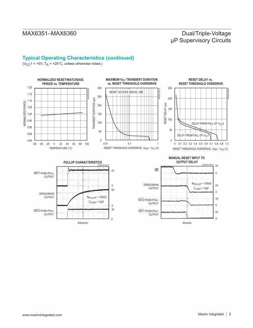
Negative-Going VCC TransientsThe MAX6351–MAX6360 are designed to ignore short negative-going VCC1 and VCC2 transients. See the Maximum VCC Transient Duration vs. Reset Threshold Overdrive graph in the Typical Operating Characteristics.
Third Input Voltage (MAX6355/MAX6356/MAX6357)The MAX6355/MAX6356/MAX6357 provide an additional input to monitor a third voltage. The threshold voltage at RSTIN is typically 1.22V. To monitor a voltage higher than 1.22V, connect a resistive divider to the circuit, as shown in Figure 2. The threshold at VEXT is:
EXT_THR1 R2V 1.22V
R2+ =
Note that RSTIN is powered by VCC1, and its voltage must therefore remain lower than or equal to VCC1.
Watchdog Input (MAX6358/MAX6359/MAX6360)The MAX6358/MAX6359/MAX6360 include a dual-mode watchdog timer to monitor μP activity. The flexible timeout architecture provides a startup mode, allowing compli-cated systems to complete lengthy boots, and a normal mode, allowing the supervisor to provide quick alerts when processor activity fails.
Figure 1. Functional Diagram Figure 2. Monitoring a Third Voltage
WATCHDOGTIMER
VCC1(5) 6
4
(5)
(5)
2GND
NOTE: PIN 1 IS RST1 FOR THE MAX6351 AND RST FOR THE MAX6352–MAX6360. PIN 5 IS RST2 FOR THE MAX6351, RSTIN FOR THE MAX6355/MAX6356/MAX6357, WDI FOR THE MAX6358/MAX6359/MAX6360, AND VCC1 FOR THE MAX6352/MAX6353/MAX6354.
VCC2
MR
(RSTIN)
RST (1)
RST2 (5)
(1)RST1
(WDI)
RESETGENERATOR
GLITCHFILTER
MAX6351–MAX6360
VTH1
VTH2
1.22V
3
VEXT
R1
R2
VCC1 ≥ VRSTIN
RSTIN
MAX6355MAX6356MAX6357
MAX6351–MAX6360 Dual/Triple-Voltage μP Supervisory Circuits
www.maximintegrated.com Maxim Integrated 7
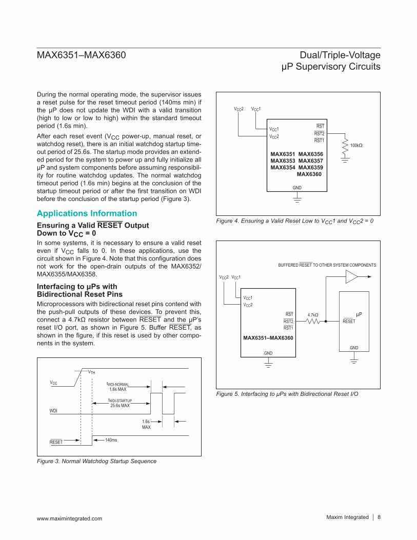
During the normal operating mode, the supervisor issues a reset pulse for the reset timeout period (140ms min) if the μP does not update the WDI with a valid transition (high to low or low to high) within the standard timeout period (1.6s min).After each reset event (VCC power-up, manual reset, or watchdog reset), there is an initial watchdog startup time-out period of 25.6s. The startup mode provides an extend-ed period for the system to power up and fully initialize all μP and system components before assuming responsibil-ity for routine watchdog updates. The normal watchdog timeout period (1.6s min) begins at the conclusion of the startup timeout period or after the first transition on WDI before the conclusion of the startup period (Figure 3).
Applications InformationEnsuring a Valid RESET Output Down to VCC = 0In some systems, it is necessary to ensure a valid reset even if VCC falls to 0. In these applications, use the circuit shown in Figure 4. Note that this configuration does not work for the open-drain outputs of the MAX6352/ MAX6355/MAX6358.
Interfacing to μPs with Bidirectional Reset PinsMicroprocessors with bidirectional reset pins contend with the push-pull outputs of these devices. To prevent this, connect a 4.7kΩ resistor between RESET and the μP’s reset I/O port, as shown in Figure 5. Buffer RESET, as shown in the figure, if this reset is used by other compo-nents in the system.
Figure 3. Normal Watchdog Startup Sequence
Figure 4. Ensuring a Valid Reset Low to VCC1 and VCC2 = 0
Figure 5. Interfacing to μPs with Bidirectional Reset I/O
1.6sMAX
tWDI-NORMAL1.6s MAX
tWDI-STARTUP25.6s MAX
VTH
VCC
WDI
RESET 140ms
VCC2 VCC1
GND
100kΩ
RST2RST1
RST
MAX6351 MAX6356MAX6353 MAX6357MAX6354 MAX6359 MAX6360
VCC2VCC1
BUFFERED RESET TO OTHER SYSTEM COMPONENTS
4.7kΩ
GND
RESETµP
GND
RST2RST1
RST
VCC2
VCC2
VCC1
VCC1
MAX6351–MAX6360
MAX6351–MAX6360 Dual/Triple-Voltage μP Supervisory Circuits
www.maximintegrated.com Maxim Integrated 8
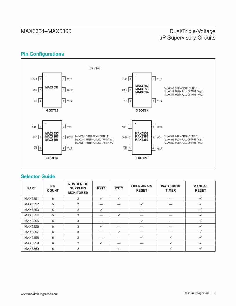
PART PINCOUNT
NUMBER OFSUPPLIES
MONITOREDRST1 RST2 OPEN-DRAIN
RESETWATCHDOG
TIMERMANUALRESET
MAX6351 6 2 ü ü — — ü
MAX6352 5 2 — — ü — ü
MAX6353 5 2 ü — — — ü
MAX6354 5 2 — ü — — ü
MAX6355 6 3 — — ü — ü
MAX6356 6 3 ü — — — ü
MAX6357 6 3 — ü — — ü
MAX6358 6 2 — — ü ü ü
MAX6359 6 2 ü — — ü ü
MAX6360 6 2 — ü — ü ü
GND
VCC2MR
1 6 VCC1
5 RST2
RST1
MAX6351
6 SOT23
TOP VIEW
2
3 4
GND
VCC2MR
1 6 VCC1
5 RSTIN
RST*
MAX6355MAX6356MAX6357
6 SOT23
2
3 4
GND
VCC2MR
*MAX6355: OPEN-DRAIN OUTPUT*MAX6356: PUSH-PULL OUTPUT (VCC1)*MAX6357: PUSH-PULL OUTPUT (VCC2)
*MAX6358: OPEN-DRAIN OUTPUT*MAX6359: PUSH-PULL OUTPUT (VCC1)*MAX6360: PUSH-PULL OUTPUT (VCC2)
*MAX6352: OPEN-DRAIN OUTPUT*MAX6353: PUSH-PULL OUTPUT (VCC1)*MAX6354: PUSH-PULL OUTPUT (VCC2)
1 6 VCC1
5 WDI
RST*
MAX6358MAX6359MAX6360
6 SOT23
2
3 4
GND
VCC2MR
1 5 VCC1RST*
MAX6352MAX6353MAX6354
5 SOT23
2
3 4
MAX6351–MAX6360 Dual/Triple-Voltage μP Supervisory Circuits
www.maximintegrated.com Maxim Integrated 9
Pin Configurations
Selector Guide
PACKAGE TYPE
PACKAGE CODE
OUTLINE NO.
LAND PATTERN NO.
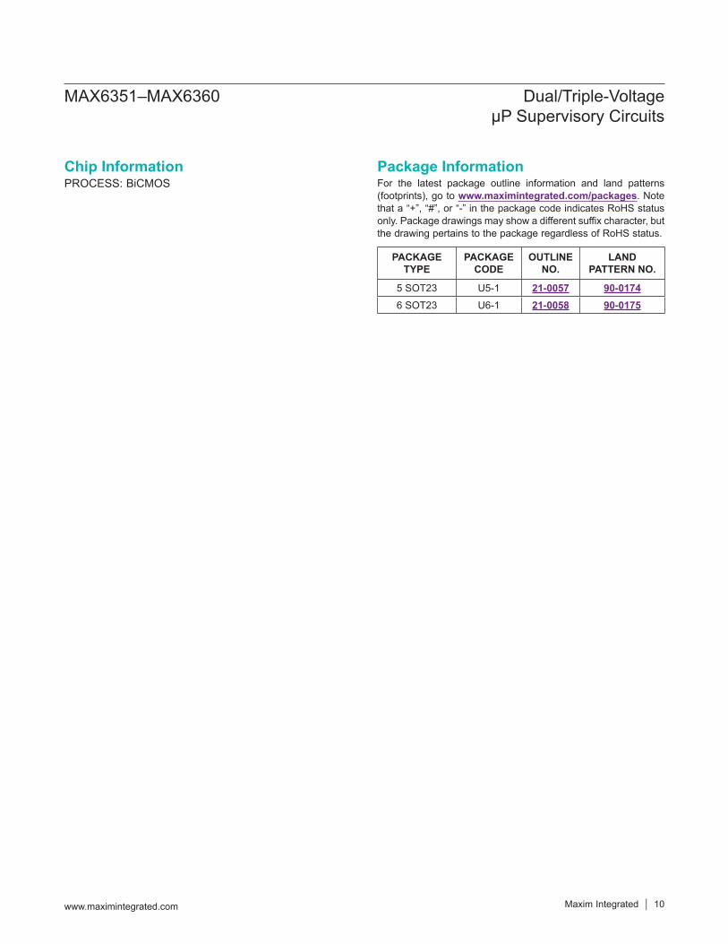
5 SOT23 U5-1 21-0057 90-01746 SOT23 U6-1 21-0058 90-0175
MAX6351–MAX6360 Dual/Triple-Voltage μP Supervisory Circuits
www.maximintegrated.com Maxim Integrated 10
Chip InformationPROCESS: BiCMOS
Package InformationFor the latest package outline information and land patterns (footprints), go to www.maximintegrated.com/packages. Note that a “+”, “#”, or “-” in the package code indicates RoHS status only. Package drawings may show a different suffix character, but the drawing pertains to the package regardless of RoHS status.
REVISIONNUMBER
REVISION DATE DESCRIPTION PAGES
CHANGED
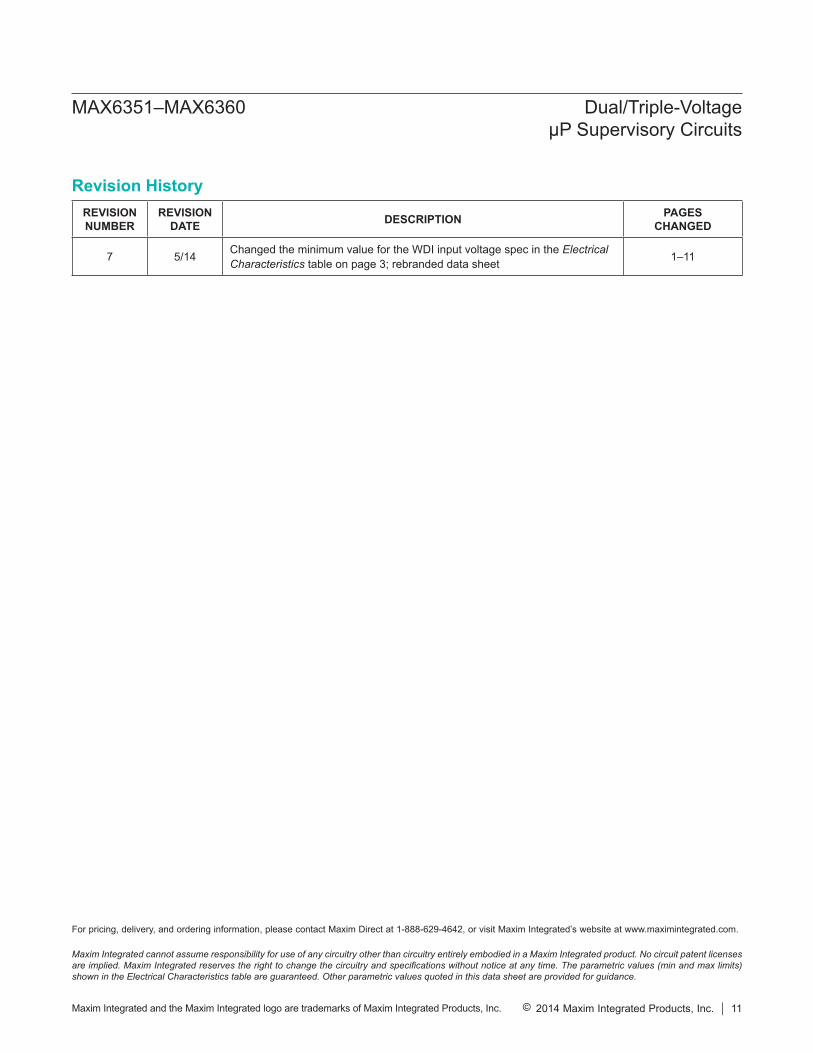
7 5/14 Changed the minimum value for the WDI input voltage spec in the Electrical Characteristics table on page 3; rebranded data sheet 1–11
Maxim Integrated cannot assume responsibility for use of any circuitry other than circuitry entirely embodied in a Maxim Integrated product. No circuit patent licenses are implied. Maxim Integrated reserves the right to change the circuitry and specifications without notice at any time. The parametric values (min and max limits) shown in the Electrical Characteristics table are guaranteed. Other parametric values quoted in this data sheet are provided for guidance.
Maxim Integrated and the Maxim Integrated logo are trademarks of Maxim Integrated Products, Inc.
MAX6351–MAX6360 Dual/Triple-Voltage μP Supervisory Circuits
© 2014 Maxim Integrated Products, Inc. 11
Revision History
For pricing, delivery, and ordering information, please contact Maxim Direct at 1-888-629-4642, or visit Maxim Integrated’s website at www.maximintegrated.com.